Äîêóìåíòàöèÿ è îïèñàíèÿ www.docs.chipfind.ru
PW
RTH
www.ti.com
FEATURES
APPLICATIONS
DESCRIPTION
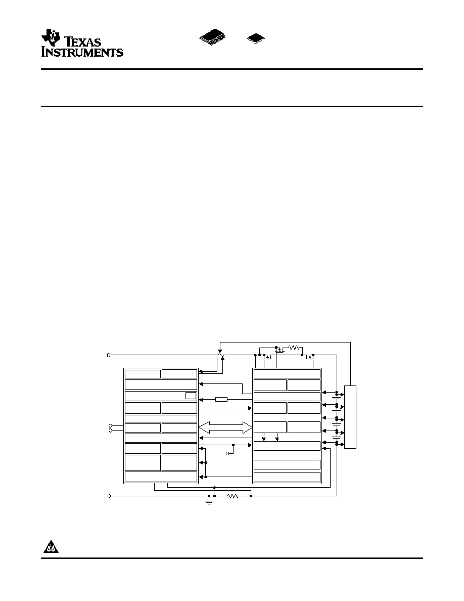
SYSTEM PARTITIONING DIAGRAM
LDO, Therm Output Drive & UVLO
Power Management
LDO, TOUT, and Power Mode control
I2C
Capacity Prediction <1% Error
SMBus
Pack +
Pack -
Discharge / Charge /
Precharge FETs
Cell and Pack
Voltage
Measurement
Precharge
FET Drive
2-Tier Overcurrent Protection
32-kHz Clock
Generator
bq2084
768 Bytes of
User Flash
Fuse
1stLevel OV and
UV Protection
Pack Undervoltage
Power Mode
Control
Precharge Control
Delay Counters
Cell Balancing Algorithm and Control
Cell Balancing
Drive
System Interface
System Watchdog
Voltage Level Translator
System Interface
32 kHz
Power Mode Control
Fail-Safe Protection
T1
1st Level OC
Protection
Temperature Measurement
<1% Error
TINT
Supply V oltage
bq29312A
PCH FET Drive
RAM Registers
SBS v1.1 Data
bq29312 RAM/Comms Validation
2 nd Level Overvolt
age Protection
XAlert
Sleep
Sense Resistor
(10 - 30 m W)
PF Input
bq29312A
SLUS629A JANUARY 2005 REVISED AUGUST 2005
TWO-CELL, THREE-CELL, AND FOUR-CELL LITHIUM-ION OR
LITHIUM-POLYMER BATTERY PROTECTION AFE
·
Notebook PCs
·
2-, 3-, or 4-Cell Series Protection Control
·
Medical and Test Equipment
·
Can Directly Interface With the bq2084 Gas
·
Portable Instrumentation
Gauges
·
Provides Individual Cell Voltages and Battery
Voltage to Battery Management Host
The bq29312A is a 2-, 3-, or 4-cell lithium-ion battery
·
Integrated Cell Balancing Drive
pack protection analog front end (AFE) IC that
·
I
2
C Compatible User Interface Allows Access
incorporates a 3.3-V, 25-mA low-dropout regulator
to Battery Information
(LDO). The bq29312A also integrates an I
2
C compat-
·
Programmable Threshold and Delay for
ible interface to extract battery parameters such as
Overload and Short Circuit During Charge and
cell voltages and control output status. Other par-
Discharge
ameters such as current protection thresholds and
delays can be programmed into the bq29312A to
·
System Alert Interrupt Output
increase the flexibility of the battery management
·
Host Control Can Initiate Sleep Power Mode
system.
and Ship Mode
The bq29312A provides safety protection for over-
·
Integrated 3.3-V, 25-mA LDO
charge,
overload,
short-circuit,
overvoltage,
and
·
Supply Voltage Range From 4.5 V to 25 V
undervoltage conditions with the battery management
host. In overload and short-circuit conditions, the
·
Low Supply Current of 60-µA Typical
bq29312A turns the FET drive off autonomously
·
bq29312A is 100% specification compatible
dependant on the internal configuration setting.
with the bq29312
Please be aware that an important notice concerning availability, standard warranty, and use in critical applications of Texas
Instruments semiconductor products and disclaimers thereto appears at the end of this data sheet.
PRODUCTION DATA information is current as of publication date.
Copyright © 2005, Texas Instruments Incorporated
Products conform to specifications per the terms of the Texas
Instruments standard warranty. Production processing does not
necessarily include testing of all parameters.
www.ti.com
DESCRIPTION (Continued)
PACKAGE DISSIPATION RATINGS
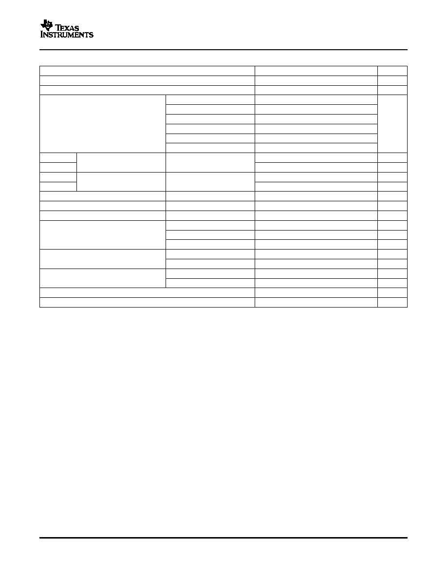
ABSOLUTE MAXIMUM RATINGS
bq29312A
SLUS629A JANUARY 2005 REVISED AUGUST 2005
These devices have limited built-in ESD protection. The leads should be shorted together or the device
placed in conductive foam during storage or handling to prevent electrostatic damage to the MOS gates.
The communications interface allows the host to observe and control the current status of the bq29312A. It
enables cell balancing, enters different power modes, sets overload levels, sets the overload blanking delay time,
sets short-circuit threshold levels for charge and discharge, and sets the short-circuit blanking delay time.
Cell balancing of each cell is performed via a cell bypass path, which is enabled via the internal control register
accessible via the I
2
C compatible interface. The maximum bypass current is set via an external series resistor
and internal FET on resistance (typical 400
).
ORDERING INFORMATION
(1)
PACKAGED
T
A
TSSOP (PW)
(2)
QFN (RTH)
(3)
40°C to 85°C
bq29312APWR-SA
bq29312ARTH
(1)
For the most current package and ordering information, see the Package Option Addendum at the end of this document, or see the TI
website at www.ti.com.
(2)
The bq29312A can be ordered in tape and reel by adding the suffix R to the orderable part number, ie: bq29312APWR bq29312ARTHR.
(3)
The QFN package is also made available in mini reel, add suffix T to the orderable part number, ie: bq29312ARTHT.
POWER RATING
POWER RATING
DERATING FACTOR
PACKAGE
T
A
25°C
ABOVE T
A
25°C
T
A
70°C
T
A
= 85°C
PW
874 mW
6.99 W/°C
559 mW
454 mW
over operating free-air temperature range unless otherwise noted
(1) (2)
bq29312A
V
CC
Supply voltage range
PACK, BAT
0.3 V to 34 V
VC1, VC2, VC3, VC4
0.3 V to 34 V
SR1, SR2
1.0 V to 1.0 V
VC5
1.0 V to 4.0 V
V
I
Input voltage range
VC1 to VC2, VC2 to VC3, VC3 to VC4, VC4 to
0.3 to 8.5 V
VC5
WDI, SLEEP, SCLK, SDATA
0.3 to 8.5 V
ZVCHG
0.3 V to 34 V
DSG, CHG
0.3 V to BAT
OD
0.3 V to 34 V
V
O
Output voltage range
PMS
0.3 V to PACK0.2 V
TOUT, SCLK, SDATA, CELL, XALERT
0.3 to 7 V
Current for cell balancing
10 mA
Continuous total power dissipation
See Dissipation Rating Table
T
stg
Storage temperature range
65°C to 150°C
Lead temperature (soldering, 10 s)
300°C
(1)
Stresses beyond those listed under "absolute maximum ratings" may cause permanent damage to the device. These are stress ratings
only, and functional operation of the device at these or any other conditions beyond those indicated under "recommended operating
conditions" is not implied. Exposure to absolute-maximum-rated conditions for extended periods may affect device reliability.
(2)
All voltages are with respect to ground of this device except VCnVC(n+1), where n = 1-, 2-, 3-, 4-cell voltage.
2
www.ti.com
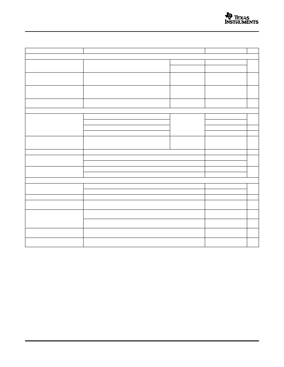
RECOMMENDED OPERATING CONDITIONS
bq29312A
SLUS629A JANUARY 2005 REVISED AUGUST 2005
MIN
NOM
MAX
UNIT
Supply Voltage (BAT or PACK)
4.5
(1)
25
V
V
I(STARTUP)
Start-up voltage (PACK)
5.0
V
VC1, VC2, VC3, VC4
0
BAT
SR1, SR2
0.5
0.5
VC5
0.5
3.0
V
I
Input voltage range
V
VCn VC(n+1), (n = 1, 2, 3, 4 )
0
5.0
PMS
0
PACK
SLEEP
0
REG
V
IH
0.8 × REG
REG
V
Logic level input voltage
SCLK, SDATA, WDI
V
IL
0
0.2 × REG
V
IH
V
(PACK)
0.2
V
(PACK)
V
PMS logic level
PMS
V
IL
0
0.2
PMS pullup/pulldown resistance
RPMS
100
1000
k
V
O
Output voltage
OD
25
V
I
O
Output current
XALERT, SDATA
200
µA
CELL
±10
µA
Input current,
I
I
SLEEP
-0.5
1.0
µA
External 3.3-V REG capacitor
C
(REG)
4.7
µF
R
(CELL)
100
Extend CELL output filter
C
(CELL)
100
nF
OD
1
mA
I
OL
Input frequency
WDI
32.768
kHz
WDI high time
2
28
µs
T
A
Operating temperature
40
85
°C
(1)
V
(PACK)
supply voltage must rise above start-up voltage on power up to enable the internal regulator which drives REG and TOUT as
required. Once V
(PACK)
is above the start-up voltage, it can fall down to the minimum supply voltage and still meet the specifications of
the bq29312A.
3
www.ti.com
ELECTRICAL CHARACTERISTICS
bq29312A
SLUS629A JANUARY 2005 REVISED AUGUST 2005
T
A
= 25°C, C
(REG)
= 4.7 µF, BAT = 14 V (unless otherwise noted)
PARAMETER
TEST CONDITIONS
MIN
TYP
MAX
UNIT
SUPPLY CURRENT
No load at REG, TOUT, XALERT, SCLK, and SDATA.
60
90
I
CC1
Supply current 1
ZVCHG = off ,VMEN = on, WDI no clock,
µA
T
A
= 25°C to 85°C
100
Select VC5 = VC4 = 0 V
Supply current
No load at REG, TOUT, XALERT, SCLK, and SDATA.
I
CC2
2(Depends of VM
T
A
= 25°C to 85°C
25
50
µA
ZVCHG = off, VMEN = off, WDI no clock
topology selected)
No load at REG, TOUT, XALERT, SCLK, and
I
(SLEEP)
Sleep current
SDATA.CHG, DSG and ZVCHG = off, REG = on,
T
A
= 25°C to 85°C
20
40
µA
VMEN = off, WDI no clock, SLEEP = REG or OPEN
REG, CHG, DSG and ZVCHG = off, REG = off,
I
(SHIP)
Ship current
T
A
= 25°C to 85°C
0.1
1.0
µA
VMEN = off, WDI no clock, VPACK= 0 V
3.3 V LDO
8.0 V < BAT or PACK
25 V, I
OUT
25 mA
4%
3.3
2%
V
6.5 V < BAT or PACK
8 V, I
OUT
25 mA
9%
3.3
2%
Regulator output
V
(REG)
T
A
= 25°C to 85°C
voltage
5.4 V
BATor PACK
6.5 V, I
O
16 mA
9%
3.3
2%
V
4.5 V
BAT or PACK
25 V, I
O
2 mA
2%
3.3
2%
V
Regulator output
V
(EGTEMP)
change with
5.4 V
BAT
25 V, I
O
= 2 mA,
T
A
= 25°C to 85°C
±0.2%
temperature
V
(REGLINE)
Line regulation
5.4 V
BAT or PACK
25 V, I
O
= 2 mA
10
20
mV
BAT = 14 V, 0.2 mA
I
O
2 mA
7
15
V
(REGLOAD)
Load regulation
mV
BAT = 14 V, 0.2 mA
I
O
25 mA
40
100
BAT = 14 V, REG = 3 V
25
100
I
MAX
Current limit
mA
BAT = 14 V, REG = 0 V
12
50
CELL VOLTAGE MONITOR
V
(Cn)
V
(Cn + 1)
= 0 V, 8 V
BAT or PACK
25 V
0.975
V
(CELL OUT)
CELL output
V
V
(Cn)
V
(Cn + 1)
= 4.5 V, 8 V
BAT or PACK
25 V
0.3
REF
CELL output
Mode
(1)
, 8 V
BAT or PACK
25 V
1%
0.975
1%
V
PACK/
PACK
CELL output
Mode
(2)
5%
5%
V
25
K = (CELL output (VC5 = 0 V, VC4 = 4.5 V) CELL
0.147
0.150
0.153
output (VC5 = VC4 = 0 V)/ 4.5
K
CELL scale factor
K = (CELL output (VC2 = 13.5 V, VC1 = 18 V) CELL output
0.147
0.150
0.153
(VC2 = VC1 = 13.5 V)/ 4.5
CELL output offset
VICR
CELL output (VC2 = 17 V, VC1 = 17 V) CELL output (VC2 = VC1 = 0 V)
1
mV
error
Cell balance internal
R
(BAL)
rds
(ON)
for internal FET switch at V
DS
= 2 V
200
400
800
resistance
(1)
Register Address =0x04, b2(CAL0) = b3(CAL1) = 1, Register Address = 0x03, b0(VMEN) = 1
(2)
Register Address = 0x03, b1(PACKOUT) = 1, b0( VMEN) = 1
4
www.ti.com
ELECTRICAL CHARACTERISTICS (Continued)
bq29312A
SLUS629A JANUARY 2005 REVISED AUGUST 2005
T
A
= 25°C, C
(REG)
= 4.7 µF, BAT = 14 V (unless otherwise noted)
PARAMETER
TEST CONDITION
MIN
NOM
MAX
UNIT
OVERLOAD (OL) AND SHORT-CIRCUIT (SC) DETECTION
V
OL
OL detection threshold range, typical
(1)
50
205
mV
V
OL
OL detection threshold program step
5
mV
V
HYS(OL)
OL detection threshold hysteresis
7
10
13
mV
Charge
100
475
V
(SC)
SC detection threshold range, typical
(2)
mV
Discharge
100
475
Charge
25
V
(SC)
SC detection threshold program step
mV
Discharge
25
V
HYS(SC)
SC detection threshold hysteresis
Charge and Discharge
40
50
60
mV
V
OL
= 50 mV (min)
40
50
60
V
(OL_acr)
OL detection threshold accuracy
(1)
Discharge
V
OL
= 100 mV
90
100
110
mV
V
OL
= 205 mV (max)
184
205
226
V
SC
= 100 mV (min)
80
100
120
V
(SC_acr)
SC detection threshold accuracy
(2)
Charge and Discharge
V
SC
= 200 mV
180
200
220
mV
V
SC
= 475 mV (max)
426
475
523
FET DRIVE CIRCUIT
V
(FETOND)
= V
(BAT)
V
(DSG)
VGS connect 1 M
BAT= 20 V
12
15
18
Output voltage, charge, and discharge
V
(FETON)
V
FETs on
V
(FETONC)
=V
(PACK)
V
(CHG)
VGS connect 1 M
PACK = 20 V
12
15
18
V
(ZCHG)
ZVCHG clamp voltage
PACK= 4.5 V
3.3
3.5
3.7
V
V
(FETOFF)
= V
(PACK)
V
(DSG)
PACK= 16 V
0.2
Output voltage, charge and discharge
V
(FETOFF)
V
FETs off
V
(FETOFF
)=V
(BAT)
V
(CHG)
BAT = 16 V
0.2
V
DSG
:10%90%
40
200
t
r
Rise time
C
L
= 4700 pF
µs
V
CHG
:10%90%
40
200
V
DSG
:90%10%
40
200
t
f
Fall time
C
L
= 4700 pF
µs
V
CHG
:90%10%
40
200
THERMISTOR DRIVE
I
O
= 1 mA at TOUT pin, rds
(ON)
= (V
REG
V
O
(TOUT))/1 mA,
r
DS(on)
TOUT pass-element series resistance
50
100
T
A
= 25°C to 85°C
LOGIC
XALERT
T
A
= 25°C to 85°C
60
100
200
R
(PUP)
Internal pullup resistance
k
SDATA, SCLK,
T
A
= 25°C to 85°C
6
10
20
XALERT, I
O
= 200 µA,
T
A
= 25°C to 85°C
0.2
V
OL
Logic level output voltage
SDATA, I
O
= 50 µA,
T
A
= 25°C to 85°C
0.4
V
OD I
O
=1 mA,
T
A
= 25°C to 85°C
0.6
(1)
See OL register for setting detection threshold
(2)
See SC register for setting detection threshold
5
Document Outline