www.ti.com
FEATURES
APPLICATIONS
DESCRIPTION
SYSTEM DIAGRAM
LDO +
Reset
I2C
SMBus
HDQ
UART
Pack +
Pack !
Discharge / Charge /
Precharge FETs
2-Tier Overcurrent
Protection
2K Bytes of
Data Flash
Fuse
Watchdog &
Protection Timing
C
e
l
l
B
a
l
a
n
c
i
n
g
D
r
i
v
e
System Interface
System Interface
32.768 kHz
16 Dig GPIO & Peripherals
8 Dig GPIO or Analog GPI
2.5 V
Nch FET Drive
(Charge Pumps)
RAM Configuration, Status
and Control Registers
24K x 22 Program
Flash
2K Bytes
of RAM
6K x 22
Mask ROM
C
e
l
l
,
B
a
t
a
n
d
P
a
c
k
V
o
l
t
a
g
e
T
r
a
n
s
l
a
t
i
o
n
Precharge
Control
H
o
s
t
I
n
t
e
r
f
a
c
e
U
A
R
T
&
D
a
t
a
M
a
n
a
g
e
m
e
n
t
TOUT and LEDOUT
Power Support
Reset
Analog Output Drive
Oscillator and PLL
T1
Internal
Only
Standard Delta-Sigma A-to-D Converter
Integrating Delta-Sigma A-to-D Converter
bq29330
SLUS673A ≠ SEPTEMBER 2005 ≠ REVISED DECEMBER 2005
2-, 3-, AND 4-CELL LITHIUM-ION OR
LITHIUM-POLYMER BATTERY PROTECTION AFE
∑
NMOS FET Drive for Charge and Discharge
FETs
∑
2- 3- or 4-Cell Series Protection Control
∑
Host Control can Initiate Sleep and Ship
∑
Can Directly Interface with the bq803x-Based
Power Modes
Gas Gauge Family
∑
Integrated 2.5-V, 16-mA LDO
∑
Watchdog and POR for the Host
∑
Integrated 3.3-V, 25-mA LDO
∑
Provides Individual Cell Voltages and Battery
Voltage to Battery Management Host
∑
Supply Voltage Range from 4.5 V to 28 V
∑
Capable of Operation With 5-m
Sense
∑
Low Supply Current of 100
µ
A Typical
Resistor Integrated Cell Balancing Drive
∑
I
2
C Compatible User Interface Allows Access
to Battery Information
∑
Notebook Computers
∑
Programmable Threshold and Delay for
∑
Medical and Test Equipment
Overload Short Circuit in Discharge and Short
∑
Instrumentation and Measurement Systems
Circuit in Charge
The bq29330 is a 2-, 3-, or 4-cell lithium-ion battery pack full-protection analog front end (AFE) IC that
incorporates a 2.5-V, 16-mA and 3.3-V, 25-mA low dropout regulator (LDO). The bq29330 also integrates an
I
2
C-compatible interface to extract battery parameters such as battery voltage, individual cell voltages, and
control output status. Other parameters such as current protection thresholds and delays can also be
programmed into the bq29330 to increase the flexibility of the battery management system.
Please be aware that an important notice concerning availability, standard warranty, and use in critical applications of Texas
Instruments semiconductor products and disclaimers thereto appears at the end of this data sheet.
PRODUCTION DATA information is current as of publication date.
Copyright © 2005, Texas Instruments Incorporated
Products conform to specifications per the terms of the Texas
Instruments standard warranty. Production processing does not
necessarily include testing of all parameters.
www.ti.com
DESCRIPTION (CONTINUED)
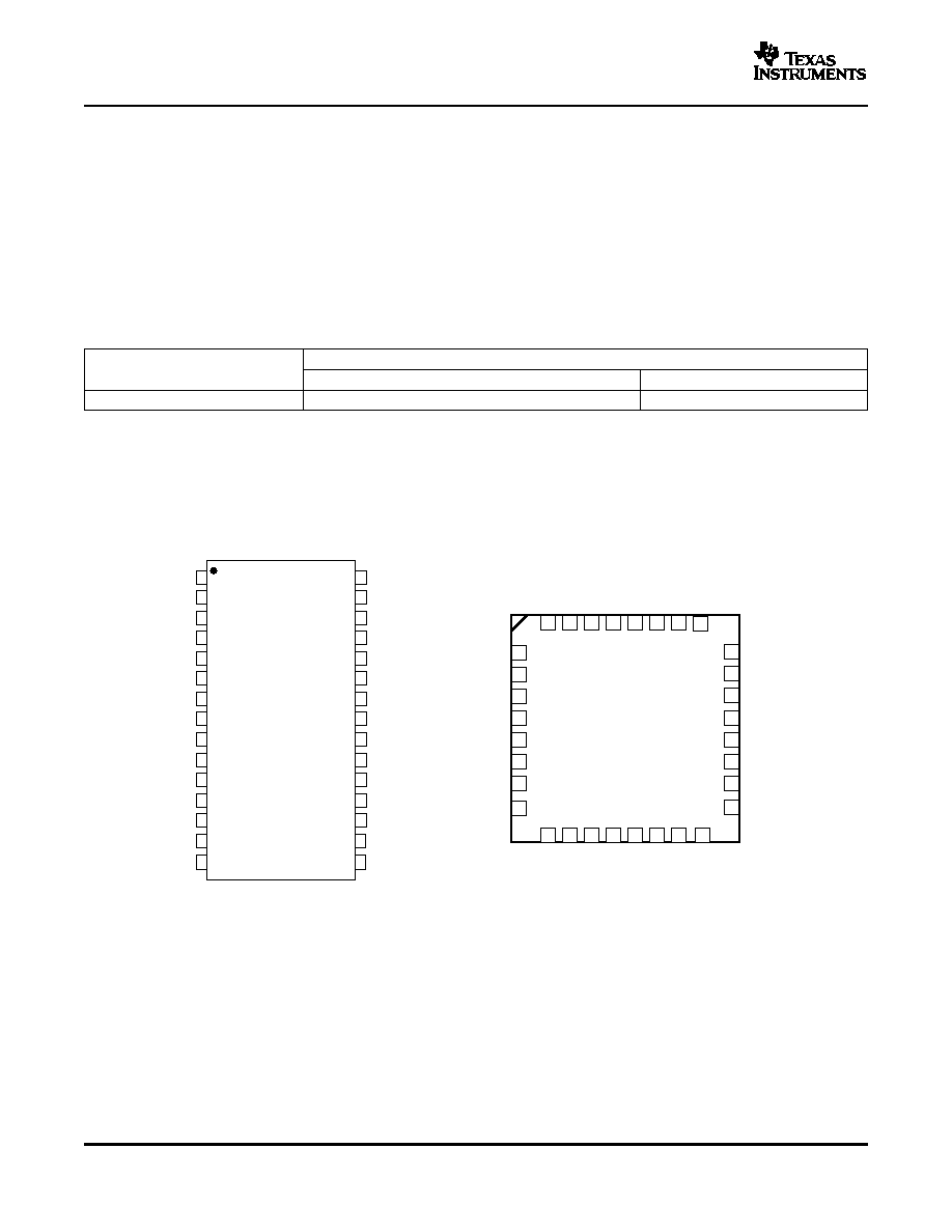
PACKAGE OPTION PIN DIAGRAMS
2
7
6
5
4
3
28
27
26
25
24
23
22
8
9
10
11
12
21
20
19
18
17
13
14
16
1
WDI
SCLK
REG
VSS
XRST
SRN
CELL-
NC
XALERT
TOUT
CELL+
PMS
GPOD
SRP
VC5
ZVCHG
VC3
VC2
DSG
PACK
VCC
CHG
SDATA
VC1
LEDOUT
VC4
VSS
15
BAT
NC
30
29
NC
TOUT
PMS
GPON
SDA
T
A
P
ACK
REG
SRP
SRN
NC
XALER
T
CHG
DSG
VC5
VC2
VC4
BA
T
NC
LEDOUT
VSS
WDI
CELL+
CELL-
VC1
VSS
NC
VCC
XRST
VC3
NC
ZVCHG
SCLK
NC
1
2
3
4
5
6
7
8
25
26
27
28
29
30
31
32
17
18
19
20
21
22
23
24
9
10
11
12 13
14
15
16
TSSOP PACKAGE
(TOP VIEW)
QFN PACKAGE
(TOP VIEW)
bq29330
SLUS673A ≠ SEPTEMBER 2005 ≠ REVISED DECEMBER 2005
The bq29330 provides safety protection for overload, short circuit in charge, and short circuit in discharge
conditions and can also provide cell overvoltage, battery overvoltage and battery undervoltage protection with the
battery management host. In overload, short circuit in charge and short circuit in discharge conditions, the
bq29330 turns off the FET drive autonomously, depending on the internal configuration setting. The
communications interface allows the host to observe and control the status of the bq29330, enable cell
balancing, enter different power modes, set current protection levels, and set the blanking delay times.
Cell balancing of each cell can be performed via a cell bypass path integrated into the bq29330, which can be
enabled via the internal control register accessible via the I
2
C-compatible interface. The maximum bypass current
is set via an external series resistor and internal FET on resistance (typ. 400
).
ORDERING INFORMATION
(1)
PACKAGE
T
A
TSSOP(DBT)
(2)
QFN(RHB)
(3)
≠40
∞
C to 110
∞
C
bq29330DBT
bq29330RHB
(1)
For the most current package and ordering information, see the Package Option Addendum at the end of this document, or see the TI
Web site at
www.ti.com
.
(2)
The bq29330 can be ordered in tape and reel by adding the suffix R to the orderable part number, i.e., bq29330DBTR, bq29330RHBR.
(3)
PRELIMINARY PACKAGE OPTION: The QFN package is also made available in mini reel; add suffix T to the orderable number, i.e.,
bq29330RHBT
2

www.ti.com
bq29330
SLUS673A ≠ SEPTEMBER 2005 ≠ REVISED DECEMBER 2005
TERMINAL FUNCTIONS
TERMINAL
DESCRIPTION
NAME
DBT NO.
RHB NO.
CELL≠
1
28
Output of scaled value of the measured cell voltage.
CELL+
2
29
Output of scaled value of the measured cell voltage.
REG
3
30
Integrated 2.5-V regulator output
VSS
4, 23
4,32
Power supply ground
XRST
5
1
Active-low output
SRN
6
2
Current sense terminal
Current sense positive terminal when charging relative to SRN; current sense negative
SRP
7
3
terminal when discharging relative to SRN
Sense voltage input terminal for most negative cell; balance current input for least positive
VC5
8
4
cell.
Sense voltage input terminal for least positive cell, balance current input for least positive cell,
VC4
9
5
and return balance current for third most positive cell.
Sense voltage input terminal for third most positive cell, balance current input for third most
VC3
10
6
positive cell, and return balance current for second most positive cell.
Sense voltage input terminal for second most positive cell, balance current input for second
VC2
11
7
most positive cell, and return balance current for most positive cell.
Sense voltage input terminal for most positive cell, balance current input for most positive cell,
VC1
12
8
and battery stack measurement input
BAT
13
10
Charge pump, charge N-CH FET gate drive
CHG
14
11
Charge pump, charge N-CH FET gate drive
DSG
16
13
Charge pump output, discharge N-CH FET gate drive
PACK
17
14
PACK positive terminal and alternative power source
VCC
19
16
Power supply voltage
ZVCHG
20
17
Connect the precharge P-CH FET drive here
GPOD
21
18
NCH FET open-drain output
PMS
22
19
Determines CHG output state on POR
LEDOUT
24
21
3.3-V output for LED display power supply
TOUT
25
22
Provides thermistor bias current
Digital input that provides the timing clock for the OC and SC delays and also acts as the
WDI
26
23
watchdog clock.
SCLK
28
25
Open-drain serial interface clock with internal 10-k
pullup to V
REG
SDATA
29
26
Open-drain bidirectional serial interface data with internal 10-k
pullup to V
REG
Open-drain output used to indicate status register changes. With internal 100-k
XALERT
30
27
pullup to V
REG
NC
15,18,27
9,12,15, 24,31
Not electrically connected to the IC
3

www.ti.com
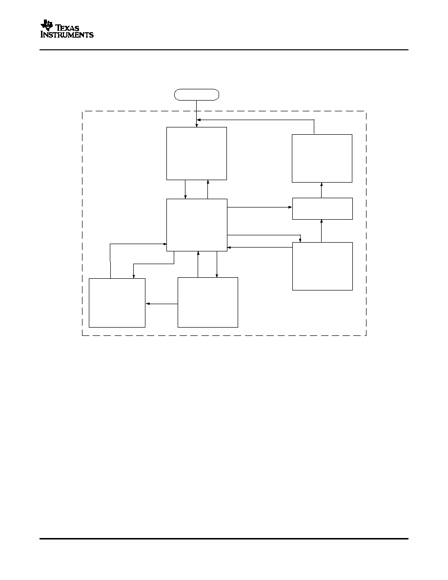
FUNCTIONAL BLOCK DIAGRAM
GND
OVERCURRENT
CELL1..4
SRP
SRN
OVERLOAD
-
COMPARATOR
SHORT CIRCUIT
COMPARATOR
SHORT_CIRCUIT
DELAY
OPEN
DRAIN
OUTPUT
WATCHDOG
TIMER
GPOD
CELL VOLTAGE
TRANSLATION
POWER
MODE
CIRCUIT
DRIVE
CONTROL
CELL+
R
SNS
C
CELL
TOUT
R
THERM
C
THERM
THERMISTOR
CELL
SELECTION
SWITCHES
2.5-V LDO
POR
SHIP_ON
SLEEP_ON
VCC
PACK
REG
C
REG
FET
LOGIC
NCH GATE
DRIVER
CHG_ON
DSG_ON
ZVCHG_ON
DSG
CHG
ZVCHG
PACK!
GG VDD
VC1
VC2
VC5
CELL 3
CELL 4
VC3
VC4
CELL 1
CELL 2
GG TS
INPUT
GG ANALOG
INPUT
WDI
32 kHz INPUT
FROM GG
GG INTERFACE
SDATA
ALERT TO GG
OPEN DRAIN
OUTPUT
GG INTERFACE
SCLK
SDATA
SCLK
XALERT
SERIAL
INTERF
ACE
STATUS
OUTPUT CTL
STATE CTL
FUNCTION CTL
CELL SEL
OLV
OLD
SCC
SCD
REGISTERS
R
ZVCHG
GATE DRIVER
0.975V
BAT/25
PACK/25
RST
GG RST
PACK+
2nd
Protection
3.3-V LDO
LEDOUT
C
LED
GG LED
INPUT
BAT
CELL!
PMS
bq29330
SLUS673A ≠ SEPTEMBER 2005 ≠ REVISED DECEMBER 2005
4
www.ti.com
SAFETY STATE DIAGRAM
No Power Supply
UVLO Mode
CHG: OFF
DSG: OFF
ZVCHG: OFF
VREG: OFF
RST: HIGH
I2 C: Disabled
Current Protection: Disabled
VCELL: Disabled
Watchdog: Disabled
Therm, Output: Disabled
Power Supply to PACK
Normal Mode
CHG: ON
DSG: ON
ZVCHG: OFF
VREG/VLED: 2.5V/3.3V
RST: Driven low after
t
RST
I2C: Enabled
Current Protection: Enabled
VCELL: Enabled
Watchdog: Enabled
Therm, Output: Enabled
LEGEND:
UVLO = Undervoltage Lock Out
KEY:
Disabled = OFF and cannot be changed via firmware
Enabled= Can be changed by firmware
Internal
VLED < 2.3 V
Firmware
Command
32 kHz Input Halted
and t WTO expired
32 kHz Resumes
Internal VLED> 2.4 V
Power Supply to PACK
Current Protection Mode
CHG: OFF
DSG: OFF
ZVCHG: OFF
VREG/VLED: 2.5 V/3.3 V
I2C: Enabled
Current Protection: Enabled
VCELL: Enabled
Watchdog: Enabled
Therm, Output: Enabled
WTO Mode
CHG: OFF
DSG: OFF
ZVCHG: OFF
RST: Pulsed
I2C: Enabled
Current Protection: Enabled
VCELL: Enabled
Watchdog: Enabled
Therm, Output: Enabled
Ship Mode
CHG: OFF
DSG: OFF
ZVCHG: OFF
I2C: Disabled
Current Protection: Disabled
VCELL: Disabled
Watchdog: Disabled
Therm, Output: Disabled
Sleep Mode
CHG: OFF
DSG: OFF
ZVCHG: OFF
I2 C: Enabled
Current Protection: Enabled
VCELL: Enabled
Watchdog: Enabled
Therm, Output: Disabled
Firmware
Command
Firmware Command
& No Supply to PACK
Firmware
Command
Firmware
Command
32 kHz Input Halted
and tWTOexpired
FirmwareCommand
VREG/VLED: 2.5 V/3.3 V
VREG/VLED: ON/ON
VREG/VLED: OFF/OFF
DSG: OFF
No supply PACK
voltage Mode
DSG: OFF
Firmware
Command
V
> V
or V
for a period of t
or t
Respectively, or V
> V
SR
OL
SCD
OL
SCD
SR
SCC
for a period
of t
SCC
bq29330
SLUS673A ≠ SEPTEMBER 2005 ≠ REVISED DECEMBER 2005
5