bq29400
bq29401
SLUS568A - JULY 2003 - REVISED OCTOBER 2003
VOLTAGE PROTECTION FOR 2 , 3 , OR 4 CELL Lion BATTERIES
(2
ND
PROTECTION)
FEATURES
D
2- ,3- , or 4-Cell Secondary
Protection
D
Low Power Consumption I
CC
< 2
m
A
(VCELL
(ALL)
< V
(PROTECT)
)
D
High Accuracy Over Sense Voltage:
-
bq29400: 4.35 V
+
25 mV
-
bq29401: 4.45 V
+
25 mV
D
Prefixed Protection Threshold Voltage
D
Programmable Delay Time
D
High Power Supply Ripple Rejection
D
Stable During Pulse Charge Operation
APPLICATIONS
D
2
nd
Level Protection in Lion Battery Packs in
-
Notebook PCs
-
Portable Instrumentation
-
Medical and Test Equipment
DESCRIPTION
The bq29400 and bq29401 are BiCMOS secondary
protection ICs for 2-, 3-, or 4-cell Lithium-Ion battery packs
that incorporate a high-accuracy precision over voltage
detection circuit. They include a programmable delay
circuit for over voltage detection time.
FUNCTION
Each cell in a multiple cell pack is compared to an internal
reference voltage. If one cell reaches an overvoltage
condition, the protection sequence begins. The bq29400
and bq29401 start charging an external capacitor through
the CD pin. When the CD pin voltage reaches 1.2 V, the
OUT pin changes from a low level to a high level.
1
2
3
4
8
7
6
5
VC1
VC2
VC3
GND
OUT
VDD
CD
VC4
PW PACKAGE
(TOP VIEW)
GND
OUT
VDD
CD
VC4
VC1
VC3
1
2
VC2
3
4
5
6
7
8
DCT PACKAGE
(TOP VIEW)
ORDERING INFORMATION
TA
V(PROTECT)
PACKAGE
TA
V(PROTECT)
MSOP (DTC)
SYMBOL
TSSOP (PW)(1)
SYMBOL
-25
∞
C to 85
∞
C
4.35 V
bq29400DCT3
CIQ
bq29400PW
2400
-25
∞
C to 85
∞
C
4.45 V
bq29401DCT3
CIR
bq29401PW
2401
(1) The bq29400 and bq29401 are available taped and reeled. Add an R suffix to the device type (e.g., bq29400PWR) to order tape
and reel version.
PRODUCTION DATA information is current as of publication date. Products
conform to specifications per the terms of Texas Instruments standard warranty.
Production processing does not necessarily include testing of all parameters.
Please be aware that an important notice concerning availability, standard warranty, and use in critical applications of Texas Instruments
semiconductor products and disclaimers thereto appears at the end of this data sheet.
www.ti.com
Copyright
2003, Texas Instruments Incorporated
bq29400
bq29401
SLUS568A - JULY 2003 - REVISED OCTOBER 2003
www.ti.com
2
These devices have limited built-in ESD protection. The leads should be shorted together or the device placed in conductive foam during
storage or handling to prevent electrostatic damage to the MOS gates.
ABSOLUTE MAXIMUM RATINGS
over operating free-air temperature range unless otherwise noted(1) (2)
UNIT
Supply voltage range
(VDD)
-0.3 V to 28 V
Input voltage range
(VC1, VC2, VC3, VC4)
-0.3 V to 28 V
Input voltage range
(VC1 to VC2, VC2 to VC3, VC3 to VC4, VC4 to GND)
-0.3 V to 8 V
Output voltage range
(OUT)
-0.3 V to 28 V
Output voltage range
(CD)
-0.3 V to 28 V
Continuous total power dissipation
See Dissipation Rating Table
Storage temperature range, Tstg
-65
∞
C to 150
∞
C
Lead temperature (soldering, 10 sec)
300
∞
C
(1) Stresses beyond those listed under "absolute maximum ratings" may cause permanent damage to the device. These are stress ratings only, and
functional operation of the device at these or any other conditions beyond those indicated under "recommended operating conditions" is not
implied. Exposure to absolute-maximum-rated conditions for extended periods may affect device reliability.
(2) All voltages are with respect to ground of this device except the differential voltage of VC1-VC2, VC2-VC3, VC3-VC4 and VC4-GND
.
PACKAGE DISSIPATION RATINGS
PACKAGE
TA
25
∞
C
POWER RATING
DERATING FACTOR
ABOVE TA = 25
∞
C
TA = 70
∞
C
POWER RATING
TA = 85
∞
C
POWER RATING
DCT
412 mW
3.3 mW/
∞
C
264 mW
214 mW
PW
525 mW
4.2 mW/
∞
C
336 mW
273 mW
RECOMMENDED OPERATING CONDITIONS
MIN
NOM
MAX
UNIT
Supply Voltage, VDD
4.0
25
V
Input voltage range, VI
VC1, VC2, VC3, VC4
0
VDD
V
Input voltage range, VI
VCn ≠ VC(n+1), (n=1, 2, 3 ), VC4-GND
0
5.0
V
Delay time capacitance, td(CD)
CD
0.22
µ
F
Voltage-monitor filter resistance
RIN
100
1k
Voltage-monitor filter capacitance
CIN
0.01
0.1
µ
F
Supply-voltage filter resistance
RVD
0
100
Supply-voltage filter capacitance
CVD
0.1
µ
F
Operating ambient temperature range, TA
-25
85
∞
C
bq29400
bq29401
SLUS568A - JULY 2003 - REVISED OCTOBER 2003
www.ti.com
3
ELECTRICAL CHARACTERISTICS
over recommended operating free-air temperature range, TA = 25
∞
C (unless otherwise noted)(1)
PARAMETER
TEST CONDITION
MIN
NOM
MAX
UNIT
V(OA)
Over voltage detection accuracy
25
35
mV
V(OA)
Over voltage detection accuracy
TA = -20
∞
C to 85
∞
C
25
50
mV
V(PROTECT) Over voltage detection voltage(1)
bq29400
4.35
V
V(PROTECT) Over voltage detection voltage(1)
bq29401
4.45
V
Vhys
Over voltage detection hysteresis(1)
300
mV
II
Input current
V2, V3 , VC4 input
VC1 = VC2 = VC3 = VC4 = 3.5 V (see Figure 1)
±
0.3
µ
A
tD1
Over voltage detection delay time
CD = 0.22
µ
F
1.0
1.5
2.0
S
I(CD_dis)
CD GND clamp current
CD = 1 V
5
12
µ
A
ICC
Supply current
VC1 = VC2 = VC3 = VC4 = 3.5 V (see Figure 1)
2.0
3.0
A
ICC
Supply current
VC1 = VC2 = VC3 = VC4 = 2.3 V (see Figure 1)
1.5
2.5
µ
A
IOH
High-level output current
OUT = 3V, VC1 = VC2 = VC3 = VC4 = 4.5 V
-1
mA
IOL
Low-level output current
OUT = 0.1 V VC1 = VC3 = VC4 = 3.5 V
5
µ
A
(1) Levels of the over-voltage detection and the hysteresis can be adjusted. For assistance contact Texas Instruments sales representative.
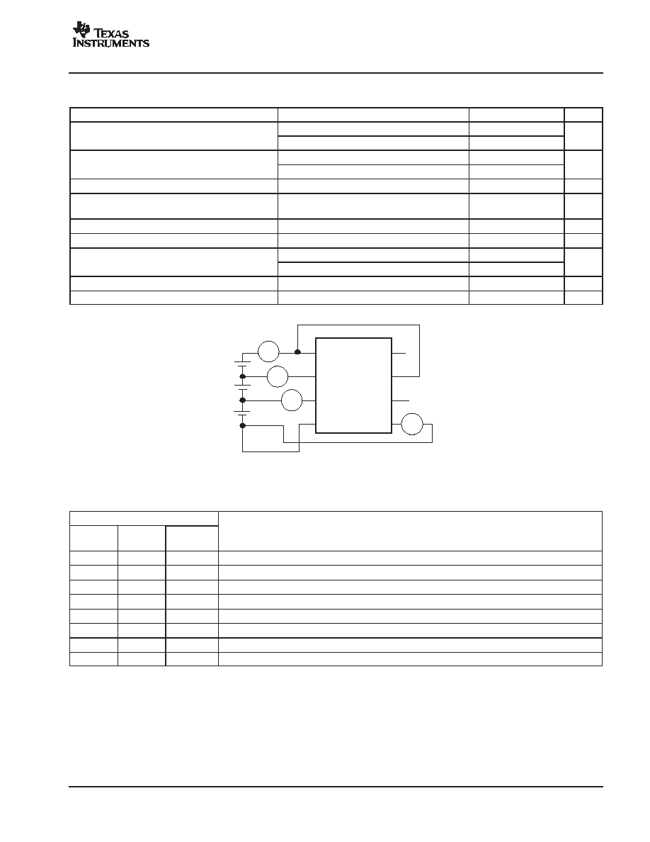
1
2
3
4
8
7
6
5
VC1
VC2
VC3
GND
OUT
VDD
CD
VC4
ICC
IIN
IIN
IIN
Figure 1. I
CC
, I
IN
Measurement (TSSOP Package)
Terminal Functions
TERMINAL NO.
MSOP
(DTC)
TSSOP
(PW)
NAME
DESCRIPTION
8
1
VC1
Sense voltage input for most positive cell
7
2
VC2
Sense voltage input for second most positive cell
6
3
VC3
Sense voltage input for third most positive cell
5
4
GND
Ground pin
4
5
VC4
Sense voltage input for least positive cell
3
6
CD
An external capacitor is connected to determine the programmable delay time
2
7
VDD
Power supply
1
8
OUT
Output
bq29400
bq29401
SLUS568A - JULY 2003 - REVISED OCTOBER 2003
www.ti.com
4
FUNCTIONAL BLOCK DIAGRAM
CIN
CIN
CIN
CIN
RIN
RIN
RIN
RIN
VC1
VC2
VC3
VC4
GND
1.2 V (TYP)
CD
VDD
OUT
ICD = 0.18
µ
A (TYP)
CVD
CDELAY
RVD
bq29400
bq29401
SLUS568A - JULY 2003 - REVISED OCTOBER 2003
www.ti.com
5
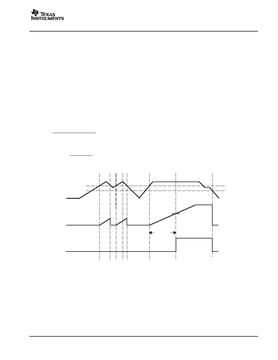
OVERVOLTAGE PROTECTION
When one of the cell voltages exceeds V
(PROTECT)
, an internal current source begins to charge the capacitor,
C
(DELAY)
, connected to the CD pin. If the voltage at the CD pin, V
CD,
reaches 1.2 V, the OUT pin is activated
and transitions high. An externally connected NCH FET is activiated and blows the external fuse in the positive
battery rail, see Figure 1, .
If all cell voltages fall below V
(PROTECT)
before the voltage at pin CD reaches 1.2 V, the delay time does not
run out. An internal switch clamps the CD pin to GND and discharges the capacitor, C
(DELAY)
, and secures the
full delay time for the next occurring overvoltage event.
Once the pin OUT is activated, it transitions back from high to low after all battery cells reach V
(PROTECT)
- V
hys.
DELAY TIME CALCULATION
The delay time is calculated as follows:
t
d
+
1.2 V
C
(DELAY)
I
CD
C
(DELAY)
+
t
d
I
CD
1.2 V
Where I
(CD)
= CD current source = 0.18
µ
A
V(PROTECT)
Cell Voltage
(VCn - VC(n-1),
VC4 - GND)
CD
OUT
1.2 V
tDELAY
V(PROTECT) - Vhys
td = (1.2 V x CDELAY)/ICD
Figure 2. Timing for Overvoltage Sensing