 | ÐлекÑÑоннÑй компоненÑ: BQ4016 | СкаÑаÑÑ:  PDF PDF  ZIP ZIP |
Äîêóìåíòàöèÿ è îïèñàíèÿ www.docs.chipfind.ru
Features
® Data retention in the absence of
power
® Automatic write-protection
during power-up/power-down
cycles
® Conventional SRAM operation;
unlimited write cycles
® 10-year minimum data retention
in absence of power
® Battery internally isolated until
power is applied
General Description
The CMOS bq4016 is a nonvolatile
8,388,608-bit static RAM organized
as 1,048,576 words by 8 bits. The in-
tegral control circuitry and lithium
energy source provide reliable non-
volatility coupled with the unlimited
write cycles of standard SRAM.
The control circuitry constantly
monitors the single 5V supply for an
out-of-tolerance condition. When V
CC
falls out of tolerance, the SRAM is
unconditionally write-protected to
prevent an inadver tent w rite
operation.
At this time the integral energy
source is switched on to sustain the
memory until after V
CC
returns
valid.
The bq4016 uses extremely low
standby current CMOS SRAMs,
coupled with a small lithium coin
cell to provide nonvolatility without
long write-cycle times and the write-
cycle limitations associated with
EEPROM.
The bq4016 has the same interface
as industry-standard SRAMs and re-
quires no external circuitry.
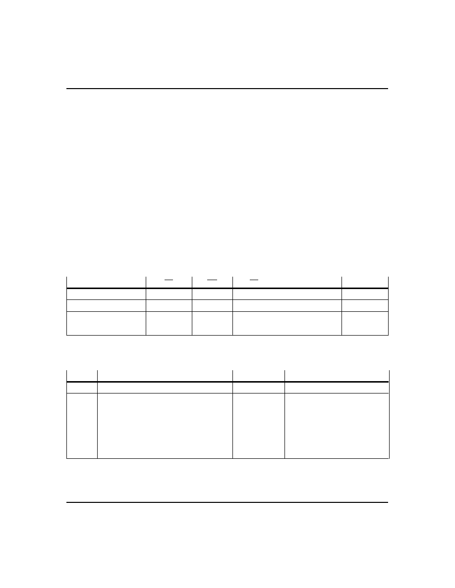
Selection Guide
Part
Number
Maximum
Access
Time (ns)
Negative
Supply
Tolerance
Part
Number
Maximum
Access
Time (ns)
Negative
Supply
Tolerance
bq4016MC -70
70
-5%
bq4016YMC -70
70
-10%
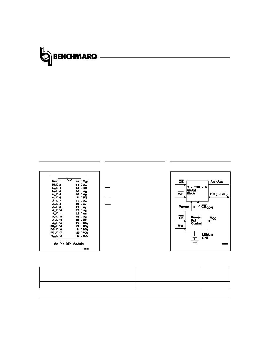
Pin Names
A
0
A
19
Address inputs
DQ
0
DQ
7
Data input/output
CE
Chip enable input
OE
Output enable input
WE
Write enable input
V
CC
+5 volt supply input
V
SS
Ground
NC
No connect
Block Diagram
1024Kx8 Nonvolatile SRAM
bq4016/bq4016Y
Sept. 1996 B
Pin Connections
1
Functional Description
When power is valid, the bq4016 operates as a standard
CMOS SRAM. During power-down and power-up cycles,
the bq4016 acts as a nonvolatile memory, automatically
protecting and preserving the memory contents.
Power-down/power-up control circuitry constantly
monitors the V
CC
supply for a power-fail-detect threshold
V
PFD
. The bq4016 monitors for V
PFD
= 4.62V typical for
use in systems with 5% supply tolerance. The bq4016Y
monitors for V
PFD
= 4.37V typical for use in systems with
10% supply tolerance.
When V
CC
falls below the V
PFD
threshold, the SRAM
automatically write-protects the data. All outputs
become high impedance, and all inputs are treated as
"don't care." If a valid access is in process at the time of
power-fail detection, the memory cycle continues to com-
pletion. If the memory cycle fails to terminate within
time t
WPT
, write-protection takes place.
As V
CC
falls past V
PFD
and approaches 3V, the control
circuitry switches to the internal lithium backup supply,
which provides data retention until valid V
CC
is applied.
When V
CC
returns to a level above the internal backup
cell voltage, the supply is switched back to V
CC
. After
V
CC
ramps above the V
PFD
threshold, write-protection
continues for a time t
CER
(120ms maximum) to allow for
processor stabilization. Normal memory operation may
resume after this time.
The internal coin cells used by the bq4016 have an
extremely long shelf life. The bq4016 provides data
retention for more than 10 years in the absence of sys-
tem power.
As shipped from Benchmarq, the integral lithium cells
are electrically isolated from the memory. (Self-discharge
in this condition is approximately 0.5% per year.)
Following the first application of V
CC
, this isolation is
broken, and the lithium backup provides data retention
on subsequent power-downs.
bq4016/bq4016Y
Truth Table
Mode
CE
WE
OE
I/O Operation
Power
Not selected
H
X
X
High Z
Standby
Output disable
L
H
H
High Z
Active
Read
L
H
L
D
OUT
Active
Write
L
L
X
D
IN
Active
Absolute Maximum Ratings
Symbol
Parameter
Value
Unit
Conditions
V
CC
DC voltage applied on V
CC
relative to V
SS
-0.3 to 7.0
V
V
T
DC voltage applied on any pin excluding V
CC
relative to V
SS
-0.3 to 7.0
V
V
T
V
CC
+ 0.3
T
OPR
Operating temperature
0 to +70
°C
T
STG
Storage temperature
-40 to +70
°C
T
BIAS
Temperature under bias
-10 to +70
°C
T
SOLDER
Soldering temperature
+260
°C
For 10 seconds
Note:
Permanent device damage may occur if Absolute Maximum Ratings are exceeded. Functional operation
should be limited to the Recommended DC Operating Conditions detailed in this data sheet. Exposure to
conditions beyond the operational limits for extended periods of time may affect device reliability.
Sept. 1996 B
2
bq4016/bq4016Y
Recommended DC Operating Conditions
(TA = 0 to 70°C)
Symbol
Parameter
Minimum
Typical
Maximum
Unit
Notes
V
CC
Supply voltage
4.5
5.0
5.5
V
bq4016Y
4.75
5.0
5.5
V
bq4016
V
SS
Supply voltage
0
0
0
V
V
IL
Input low voltage
-0.3
-
0.8
V
V
IH
Input high voltage
2.2
-
V
CC
+ 0.3
V
Note:
Typical values indicate operation at T
A
= 25°C.
DC Electrical Characteristics
(TA = 0 to 70°C, VCCmin
VCC
VCCmax)
Symbol
Parameter
Minimum
Typical
Maximum
Unit
Conditions/Notes
I
LI
Input leakage current
-
-
±
2
µ
A
V
IN
= V
SS
to V
CC
I
LO
Output leakage current
-
-
±
2
µ
A
CE = V
IH
or OE = V
IH
or
WE = V
IL
V
OH
Output high voltage
2.4
-
-
V
I
OH
= -1.0 mA
V
OL
Output low voltage
-
-
0.4
V
I
OL
= 2.1 mA
I
SB1
Standby supply current
-
5
12
mA
CE = V
IH
I
SB2
Standby supply current
-
2.5
5
mA
0V
V
IN
0.2V,
CE
V
CC
- 0.2V,
or V
IN
V
CC
- 0.2
I
CC
Operating supply current
-
75
115
mA
Min. cycle, duty = 100%,
CE = V
IL
,I
I/O
= 0mA,
A19 < V
IL
or A19 > V
IH
,
V
PFD
Power-fail-detect voltage
4.55
4.62
4.75
V
bq4016
4.30
4.37
4.50
V
bq4016Y
V
SO
Supply switch-over voltage
-
3
-
V
Note:
Typical values indicate operation at T
A
= 25°C, V
CC
= 5V.
Sept. 1996 B
3
bq4016/bq4016Y
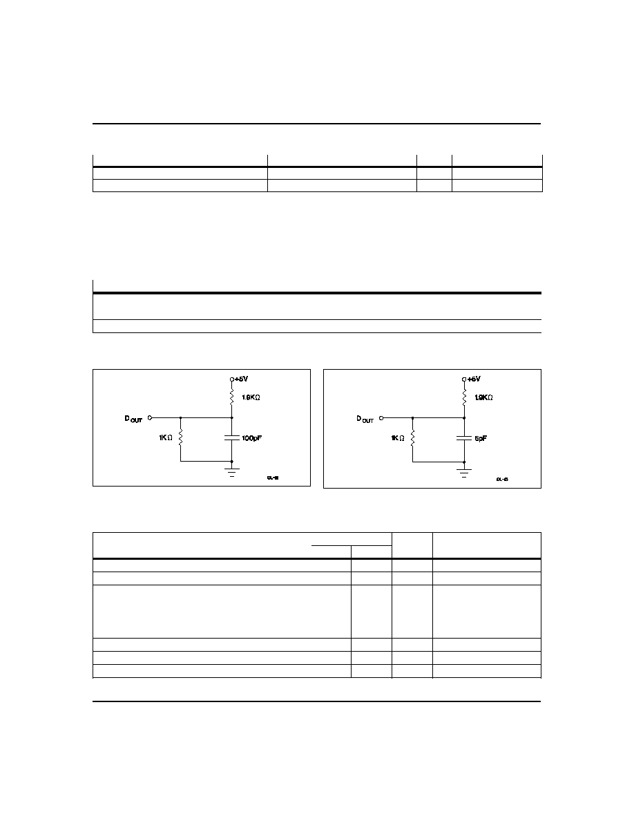
AC Test Conditions
Parameter
Test Conditions
Input pulse levels
0V to 3.0V
Input rise and fall times
5 ns
Input and output timing reference levels
1.5 V (unless otherwise specified)
Figure 2. Output Load B
Figure 1. Output Load A
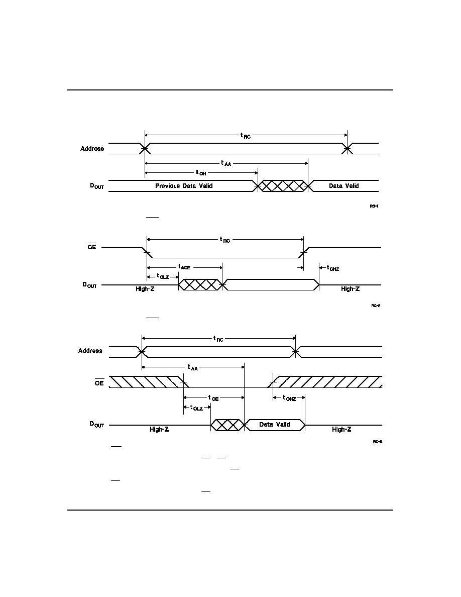
Read Cycle
(TA = 0 to 70°C, VCCmin
VCC
VCCmax)
Symbol
Parameter
-70
Unit
Conditions
Min.
Max.
t
RC
Read cycle time
70
-
ns
t
AA
Address access time
-
70
ns
Output load A
t
ACE
Chip enable access time
-
70
ns
Output load A
t
OE
Output enable to output valid
-
35
ns
Output load A
t
CLZ
Chip enable to output in low Z
5
-
ns
Output load B
t
OLZ
Output enable to output in low Z
5
-
ns
Output load B
t
CHZ
Chip disable to output in high Z
0
25
ns
Output load B
t
OHZ
Output disable to output in high Z
0
25
ns
Output load B
t
OH
Output hold from address change
10
-
ns
Output load A
Sept. 1996 B
Capacitance
(TA = 25°C, F = 1MHz, VCC = 5.0V)
Symbol
Parameter
Minimum
Typical
Maximum
Unit
Conditions
C
I/O
Input/output capacitance
-
-
20
pF
Output voltage = 0V
C
IN
Input capacitance
-
-
20
pF
Input voltage = 0V
Note:
These parameters are sampled and not 100% tested.
4
bq4016/bq4016Y
Sept. 1996 B
Read Cycle No. 2 (CE Access)
1,3,4
Read Cycle No. 1 (Address Access)
1,2
Notes: 1.
WE is held high for a read cycle.
2.
Device is continuously selected: CE = OE = V
IL
.
3. Address is valid prior to or coincident with CE transition low.
4. OE = V
IL
.
5.
Device is continuously selected: CE = V
IL
.
Read Cycle No. 3 (OE Access)
1,5
5