Enhanced_RTC_With_NVRAM_Control
Features
® Direct clock/calendar replace-
ment for IBM
®
AT-compatible
computers and other applications
® 114 bytes of general nonvolatile
storage
® Enhanced features include:
-
System wake-up capability--
alarm interrupt output active
in battery-backup mode
-
2.73.6V operation (bq4285L);
4.55.5V operation (bq4285E)
-
32kHz output for power
management
® Automatic backup and write-
protect control to external SRAM
® Functionally compatible with the
DS1285
® Less than 0.5
µ
A load under bat-
tery operation
® Selectable Intel or Motorola bus
timing (PLCC), Intel bus timing
(DIP and SOIC)
® 14 bytes for clock/calendar and
control
® BCD or binary format for clock
and calendar data
® Calendar in day of the week, day
of the month, months, and years,
with automatic leap-year adjust-
ment
® Time of day in seconds, minutes,
and hours
-
12- or 24-hour format
-
Optional daylight saving
adjustment
® Programmable square wave out-
put
® Three individually maskable in-
terrupt event flags:
-
Periodic rates from 122
µ
s to
500ms
-
Time-of-day alarm once per
second to once per day
-
End-of-clock update cycle
® 24-pin plastic DIP or SOIC
General Description
The CMOS bq4285E/L is a low-power
microprocessor peripheral providing a
time-of-day clock and 100-year calen-
dar with alarm features and battery
operation. Other features include
three maskable interrupt sources,
square wave output, and 114 bytes of
general nonvolatile storage.
A 32.768kHz output is available for
sustaining power-management activi-
ties. Wake-up capability is provided by
an alarm interrupt, which is active in
battery-backup mode.
The bq4285E/L write-protects the
clock, calendar, and storage registers
during power failure. A backup bat-
tery then maintains data and oper-
ates the clock and calendar.
The bq4285E/L is a fully compatible
r e a l - t i m e cl o ck f o r I B M AT-
compatible computers and other ap-
plications. The only external compo-
nents are a 32.768kHz crystal and a
backup battery.
T h e
b q 4 2 8 5 E / L
i n t e g r a t e s
a
battery-backup controller to make a
1
PN428502.eps
28-Pin PLCC
5
6
7
8
9
10
11
25
24
23
22
21
20
19
4
3
2
1
28
27
26
12
13
14
15
16
17
18
AD0
AD1
AD2
AD3
AD4
AD5
NC
AD
6
NC
AD
7
V
SS
CS
AS
NC
CEIN
BC
INT
RST
DS
VSS
R/ W
X2
X1
MOT
V
OUT
V
CC
SQW
CE
OUT
Pin Names
AD
0
AD
7
Multiplexed address/data
input/output
MOT
Bus type select input
(PLCC only )
CS
Chip select input
AS
Address strobe input
DS
Data strobe input
R/W
Read/write input
INT
Interrupt request output
RST
Reset input
SQW
Square wave output
BC
3V backup cell input
X1X2
Crystal inputs
NC
No connect
CE
IN
RAM chip enable input
CE
OUT
RAM chip enable output
V
OUT
Supply output
V
CC
+5V supply
bq4285E/L
1
PN428501.eps
24-Pin DIP or SOIC
2
3
4
5
6
7
8
24
23
22
21
20
19
18
17
9
10
16
15
11
12
14
13
VCC
SQW
CEOUT
BC
INT
RST
DS
VSS
R/W
AS
CS
VOUT
X1
X2
AD0
AD1
AD2
AD3
AD4
AD5
AD6
AD7
VSS
CEIN
Pin Connections
Enhanced RTC With NVRAM Control
Jan. 1999 B
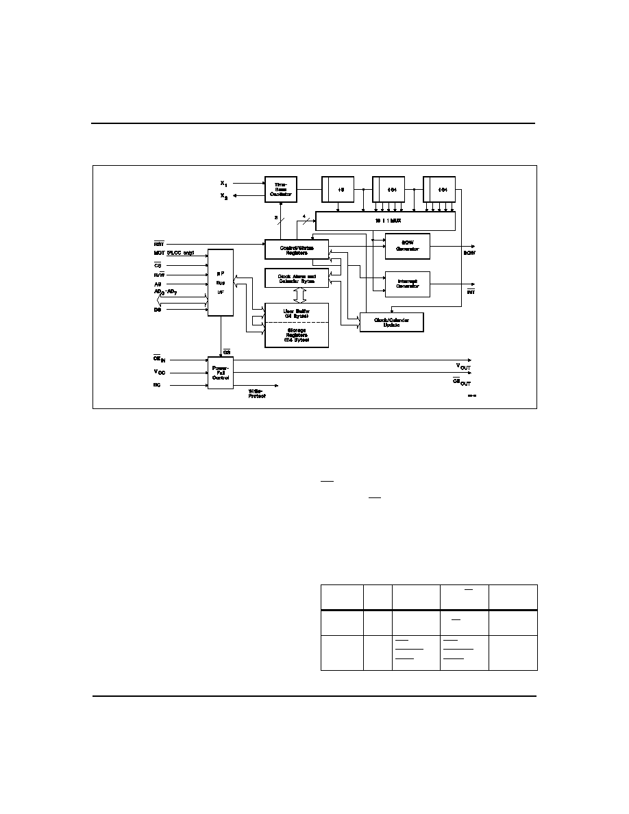
Block Diagram
standard CMOS SRAM nonvolatile during power-fail
conditions. During power-fail, the bq4285E/L auto-
matically write-protects the external SRAM and pro-
vides a V
CC
output sourced from the clock backup
battery.
Pin Descriptions
AD
0
AD
7
Multiplexed address/data input/
output
The bq4285E/L bus cycle consists of two
phases: the address phase and the data-
transfer phase. The address phase precedes
the data-transfer phase.
During the ad-
dress phase, an address placed on AD
0
AD
7
is latched into the bq4285E/L on the falling
edge of the AS signal.
During the data-
transfer phase of the bus cycle, the AD
0
AD
7
pins serve as a bidirectional data bus.
MOT
Bus type select input (PLCC package
only)
MOT selects bus timing for either Motorola
or Intel architecture.
This pin should be
tied to V
CC
for Motorola timing or to V
SS
for
Intel timing (see Table 1).
The setting should not be changed during
system operation. MOT is internally pulled
low by a 20K
resistor. For the DIP and
SOIC packages, this pin is internally con-
nected to V
SS
, enabling the bus timing for
the Intel architecture.
CS
Chip select input
CS should be driven low and held stable
during the data-transfer phase of a bus cy-
cle accessing the bq4285E/L.
2
Bus
Type
MOT
Level
DS
Equivalent
R/W
Equivalent
AS
Equivalent
Motorola
V
CC
DS, E, or
2
R/W
AS
Intel
V
SS
RD,
MEMR, or
I/OR
WR,
MEMW, or
I/OW
ALE
Table 1. Bus Setup
Jan. 1999 B
bq4285E/L

AS
Address strobe input
AS serves to demultiplex the address/data
bus. The falling edge of AS latches the ad-
dress on AD
0
AD
7
. This demultiplexing pro-
cess is independent of the CS signal. For DIP,
SOIC, and PLCC packages with MOT = V
CC
,
the AS input is provided a signal similar to
ALE in an Intel-based system.
DS
Data strobe input
For DIP, SOIC, and PLCC packages with
MOT = V
SS
, the DS input is provided a sig-
nal similar to RD, MEMR, or I/OR in an
Intel-based system. The falling edge on DS
is used to enable the outputs during a read
cycle.
For the PLCC package, when MOT = V
CC
,
D S c o n t r o l s d a t a t r a n s f e r d u r i n g a
bq4285E/L bus cycle. During a read cycle,
the bq4285E/L drives the bus after the ris-
ing edge on DS. During a write cycle, the
falling edge on DS is used to latch write
data into the chip.
R/W
Read/write input
For DIP, SOIC, and PLCC packages with
MOT = V
SS
, R/W is provided a signal simi-
lar to WR, MEMW, or I/OW in an Intel-
based system.
The rising edge on R/W
latches data into the bq4285E/L.
For the PLCC package, when MOT = V
CC
,
the level on R/W identifies the direction of
data transfer. A high level on R/W indicates
a read bus cycle, whereas a low on this pin
indicates a write bus cycle.
INT
Interrupt request output
INT is an open-drain output. This allows
INT to be valid in battery-backup mode for
the alarm interrupt.
To use this feature,
INT must be connected to a power supply
other than V
CC
. INT is asserted low when
any event flag is set and the corresponding
event enable bit is also set. INT becomes
high-impedance whenever register C is read
(see the Control/Status Registers section).
RST
Reset input
The bq4285E/L is reset when RST is pulled
low.
When reset, INT becomes high-
impedance, and the bq4285E/L is not accessi-
ble. Table 4 in the Control/Status Registers
section lists the register bits that are cleared
by a reset.
Reset may be disabled by connecting RST to
V
CC
. This allows the control bits to retain their
states through power-down/power-up cycles.
SQW
Square-wave output
SQW may output a programmable fre-
quency square-wave signal during normal
(V
CC
valid) system operation. Any one of
the 13 specific frequencies may be selected
through register A.
This pin is held low
when the square-wave enable bit (SQWE)
in register B is 0 (see the Control/Status
Registers section).
A 32.768kHz output is enabled by setting
the SQWE bit in register B to 1 and the
32KE bit in register C to 1 after setting
OSC2OSC0 in register A to 011 (binary).
BC
3V backup cell input
BC should be connected to a 3V backup cell
for RTC operation and storage register non-
volatility in the absence of power. When V
CC
slews down past V
BC
(3V typical), the inte-
gral control circuitry switches the power
source to BC. When V
CC
returns above V
BC
,
the power source is switched to V
CC
.
Upon power-up, a voltage within the V
BC
range must be present on the BC pin for
the oscillator to start up.
X1X2
Crystal inputs
The X1X2 inputs are provided for an ex-
ternal 32.768Khz quartz crystal, Daiwa
DT-26 or equivalent, with 6pF load capaci-
tance. A trimming capacitor may be neces-
sary for extremely precise time-base gen-
eration.
CE
IN
External RAM chip enable input,
active low
CE
IN
should be driven low to enable the
controlled external RAM. CE
IN
is internally
pulled up with a 50K
resistor.
CE
OUT
External RAM chip enable output,
active low
When power is valid, CE
OUT
reflects CE
IN.
V
OUT
Supply output
V
OUT
provides the higher of V
CC
or V
BC
,
switched internally, to supply external RAM.
V
CC
Positive power supply
V
SS
Ground
3
Jan. 1999 B
bq4285E/L
Functional Description
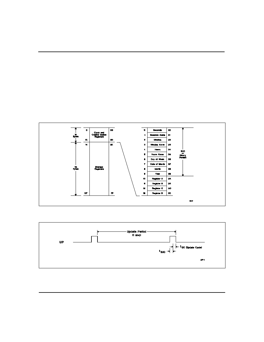
Address Map
The bq4285E/L provides 14 bytes of clock and con-
trol/status registers and 114 bytes of general nonvolatile
storage.
Figure 1 illustrates the address map for the
bq4285L.
Update Period
The update period for the bq4285E/L is one second. The
bq4285E/L updates the contents of the clock and calen-
dar locations during the update cycle at the end of each
update period (see Figure 2). The alarm flag bit may
also be set during the update cycle.
The bq4285E/L copies the local register updates into the
user buffer accessed by the host processor. When a 1 is
written to the update transfer inhibit bit (UTI) in regis-
ter B, the user copy of the clock and calendar bytes re-
mains unchanged, while the local copy of the same bytes
continues to be updated every second.
The update-in-progress bit (UIP) in register A is set
t
BUC
time before the beginning of an update cycle (see
Figure 2). This bit is cleared and the update-complete
flag (UF) is set at the end of the update cycle.
4
Figure 1. Address Map
Figure 2. Update Period Timing and UIP
Jan. 1999 B
bq4285E/L

Programming the RTC
The time-of-day, alarm, and calendar bytes can be written
in either the BCD or binary format (see Table 2).
These steps may be followed to program the time, alarm,
and calendar:
1.
Modify the contents of register B:
a.
Write a 1 to the UTI bit to prevent trans-
fers between RTC bytes and user buffer.
b.
Write the appropriate value to the data for-
mat (DF) bit to select BCD or binary format
for all time, alarm, and calendar bytes.
c.
Write the appropriate value to the hour
format (HF) bit.
2.
Write new values to all the time, alarm, and
calendar locations.
3.
Clear the UTI bit to allow update transfers.
On the next update cycle, the RTC updates all 10 bytes
in the selected format.
Square-Wave Output
The bq4285E/L divides the 32.768kHz oscillator fre-
quency to produce the 1 Hz update frequency for the
clock and calendar. Thirteen taps from the frequency di-
vider are fed to a 16:1 multiplexer circuit. The output of
this mux is fed to the SQW output and periodic inter-
rupt generation circuitry. The four least-significant bits
of register A, RS0RS3, select among the 13 taps (see
Table 3). The square-wave output is enabled by writing
a 1 to the square-wave enable bit (SQWE) in register B.
A 32.768kHz output may be selected by setting
OSC2OSC0 in register A to 011 while SQWE = 1 and
32KE = 1.
5
bq4285E/L
Jan. 1999 B
Address
RTC Bytes
Range
Decimal
Binary
Binary-Coded
Decimal
0
Seconds
059
00H3BH
00H59H
1
Seconds alarm
059
00H3BH
00H59H
2
Minutes
059
00H3BH
00H59H
3
Minutes alarm
059
00H3BH
00H59H
4
Hours, 12-hour format
112
01HOCH AM;
81H8CH PM
01H12H AM;
81H92H PM
Hours, 24-hour format
023
00H17H
00H23H
5
Hours alarm, 12-hour format
112
01HOCH AM;
81H8CH PM
01H12H AM;
81H92H PM
Hours alarm, 24-hour format
023
00H17H
00H23H
6
Day of week (1=Sunday)
17
01H07H
01H07H
7
Day of month
131
01H1FH
01H31H
8
Month
112
01H0CH
01H12H
9
Year
099
00H63H
00H99H
Table 2. Time, Alarm, and Calendar Formats