www.ti.com
PRODUCTION DATA information is current as of publication date.
Products conform to specifications per the terms of Texas Instruments
standard warranty. Production processing does not necessarily include
testing of all parameters.
Copyright © 2001-2004, Texas Instruments Incorporated
Please be aware that an important notice concerning availability, standard warranty, and use in critical applications of
Texas Instruments semiconductor products and disclaimers thereto appears at the end of this data sheet.
All trademarks are the property of their respective owners.
BUF04701
SBOS214B ≠ SEPTEMBER 2001 ≠ REVISED JULY 2004
DESCRIPTION
The BUF04701 is a 4-channel, low-power, high-voltage rail-
to-rail input/output buffer. Operating on supplies ranging from
3.5V to 12V (
±
1.75V to
±
6V), the BUF04701 has a 3dB
bandwidth of 8MHz with a slew rate of 10V/
µ
s, and requires
only 1.1mA quiescent current. The BUF04701 features rail-
to-rail input and output capability, giving maximum dynamic
range at any supply voltage.
Featuring fast slewing and settling times, as well as a high
output drive, the BUF04701 is ideal for use as a voltage
reference buffer in Thin Film Transistor Liquid Crystal Dis-
plays (TFT-LCDs).
The BUF04701 is available in an MSOP-10 package, provid-
ing the smallest footprint and thinnest package option avail-
able, as well as the TSSOP-14 package with a pinout that
corresponds to standard quad op amps. This makes it easy to
replace quad op amps in existing LCD displays with the low
cost BUF04701, without changing the layout. The BUF04701
operates over a temperature range of ≠40
∞
C to +125
∞
C.
FEATURES
q
UNITY GAIN BUFFER
q
RAIL-TO-RAIL INPUT/OUTPUT
q
WIDE BANDWIDTH: 8MHz
q
HIGH SLEW RATE: 10V/
µ
s
q
LOW QUIESCENT CURRENT: 1.1mA
q
TINY PACKAGE: MSOP-10, TSSOP-14
4-Channel, Rail-to-Rail, CMOS
BUFFER AMPLIFIER
APPLICATIONS
q
TFT-LCD REFERENCE DRIVERS
q
NOTEBOOKS
q
ELECTRONIC GAMES
q
ELECTRONIC BOOKS
q
PERSONAL COMMUNICATION DEVICES
q
PDA
q
ACTIVE FILTERS
q
ADC/DAC BUFFER
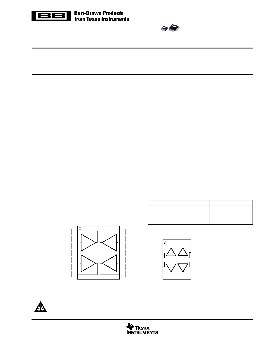
1
2
3
4
5
10
9
8
7
6
Out D
In D
≠V
In C
Out C
Out A
In A
+V
In B
Out B
MSOP-10 (DGS)
1
2
3
4
5
6
7
14
13
12
11
10
9
8
Out D
NC
(1)
In D
≠V
In C
NC
(1)
Out C
Out A
NC
(1)
In A
+V
In B
NC
(1)
Out B
TSSOP-14 (PW)
A
C
B
D
BUF04701 RELATED PRODUCTS
FEATURES
PRODUCT
1.2 MHz BW, 3.3mA I
Q
BUF11702
7MHz GBW, 1.5mA I
Q
, V
S
3.5 - 12
OPA4743
5.9MHz GBW, 4.5mA I
Q
, V
S
= 4V - 44V
TLE2144/2
10MHz GBW, 2.5mA I
Q
, 16V/
µ
s SR
TLC084
NOTE: (1) NC Means No Internal Connection
Æ
0470
1A
BUF04701
2
SBOS214B
www.ti.com
Supply Voltage, V+ to V≠ ................................................................. 13.2V
Signal Input Terminals, Voltage
(2)
................... (V≠) ≠0.5V to (V+) + 0.5V
Current
(2)
.................................................... 10mA
Output Short-Circuit
(3)
.............................................................. Continuous
Operating Temperature .................................................. ≠40
∞
C to +125
∞
C
Storage Temperature ..................................................... ≠65
∞
C to +150
∞
C
Junction Temperature .................................................................... +150
∞
C
Lead Temperature (soldering, 10s) ............................................... +300
∞
C
NOTES: (1) Stresses above these ratings may cause permanent damage.
Exposure to absolute maximum conditions for extended periods may
degrade device reliability. (2) Input terminals are diode-clamped to the
power-supply rails. Input signals that can swing more than 0.5V beyond the
supply rails should be current-limited to 10mA or less. (3) Short-circuit to
ground, one amplifier per package.
ABSOLUTE MAXIMUM RATINGS
(1)
ELECTROSTATIC
DISCHARGE SENSITIVITY
This integrated circuit can be damaged by ESD. Texas Instru-
ments recommends that all integrated circuits be handled with
appropriate precautions. Failure to observe proper handling
and installation procedures can cause damage.
ESD damage can range from subtle performance degrada-
tion to complete device failure. Precision integrated circuits
may be more susceptible to damage because very small
parametric changes could cause the device not to meet its
published specifications.
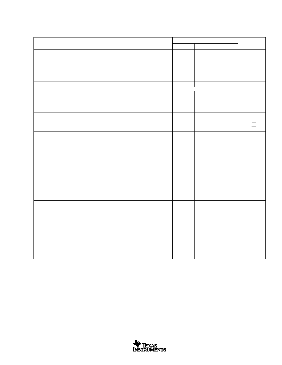
SPECIFIED
PACKAGE
TEMPERATURE
PACKAGE
ORDERING
TRANSPORT
PRODUCT
PACKAGE-LEAD
DESIGNATOR
RANGE
MARKING
NUMBER
MEDIA, QUANTITY
Quad
BUF04701
MSOP-10
DGS
≠40
∞
C to +125
∞
C
BUF04701
BUF04701AIDGSR
Tape and Reel, 2500
BUF04701
TSSOP-14
PW
≠40
∞
C to +125
∞
C
04701A
BUF04701AIPWR
Tape and Reel, 2500
NOTE: (1) For the most current package and ordering information, see the Package Option Addendum located at the end of this data sheet.
PACKAGE/ORDERING INFORMATION
(1)
BUF04701
3
SBOS214B
www.ti.com
PARAMETER
CONDITION
MIN
TYP
MAX
UNITS
OFFSET VOLTAGE
Input Offset Voltage
V
OS
V
S
=
±
5, V
CM
= 0
±
1.5
±
7
mV
Drift
dV
OS
/dT
±
8
µ
V/
∞
C
vs Power Supply
PSRR
V
S
= 3.5V to 12V, V
CM
= V
S
/2 ≠ 0.5V
20
100
µ
V/V
Over Temperature
V
S
= 3.5V to 12V, V
CM
= V
S
/2 ≠ 0.5V
200
µ
V/V
Channel Separation, DC
1
µ
V/V
f = 10kHz
110
dB
INPUT VOLTAGE RANGE
Common-Mode Voltage Range
V
CM
Limited by Output Range
INPUT BIAS CURRENT
Input Bias Current
I
B
V
CM
= V
S
/2
1
±
10
pA
INPUT IMPEDANCE
Common-Mode
5 ∑ 10
12
|| 4
|| pF
NOISE
Input Voltage Noise, f = 0.1Hz to 10Hz
V
S
=
±
6V, V
CM
= 0
11
µ
Vrms
Input Voltage Noise Density, f = 10kHz
e
n
V
S
=
±
6V, V
CM
= 0
30
nV/
Hz
Input Current Noise Density, f = 1kHz
i
n
V
S
=
±
6V, V
CM
= 0
2.5
fA/
Hz
TRANSFER CHARACTERISTIC
Gain
0.9975
1.000
1.0025
over Temperature
0.995
1.000
1.005
OUTPUT
Voltage Output Swing from Rail
R
L
= 10k
75
mV
R
L
= 2k
150
200
mV
over Temperature
R
L
= 2k
250
mV
Short-Circuit Current
I
SC
±
32
mA
FREQUENCY RESPONSE
C
L
= 10pF
Bandwidth ≠3dB
BW
8
MHz
Slew Rate
SR
V
S
=
±
6V
10
V/
µ
s
Settling Time, 0.1%
t
S
V
S
=
±
6V, 5V Step
9
µ
s
Overload Recovery Time
V
IN
= V
S
0.2
µ
s
Total Harmonic Distortion + Noise
THD+N
V
S
=
±
6V, V
O
= 1Vrms, G = 1,
0.001
%
f = 6kHz, V
CM
= V
S
/2
POWER SUPPLY
Specified Voltage Range, Single Supply
V
S
3.5
12
V
Specified Voltage Range, Dual Supplies
±
1.75
±
6
V
Operating Voltage Range
+3.5 to +12
V
Quiescent Current (per amplifier)
I
Q
I
O
= 0
1.1
1.5
mA
over Temperature
1.7
mA
TEMPERATURE RANGE
Specified Range
≠40
+125
∞
C
Operating Range
≠40
+125
∞
C
Storage Range
≠65
+150
∞
C
Thermal Resistance
JA
TSSOP Surface Mount
100
∞
C/W
MSOP Surface Mount
200
∞
C/W
BUF04701
ELECTRICAL CHARACTERISTICS: V
S
= +3.5V to +12V
Boldface limits apply over the specified temperature range, T
A
= ≠40
∞
C to +125
∞
C
At T
A
= +25
∞
C, R
L
= 10k
connected to V
S
/ 2 and V
OUT
= V
S
/ 2, unless otherwise noted.
BUF04701
4
SBOS214B
www.ti.com
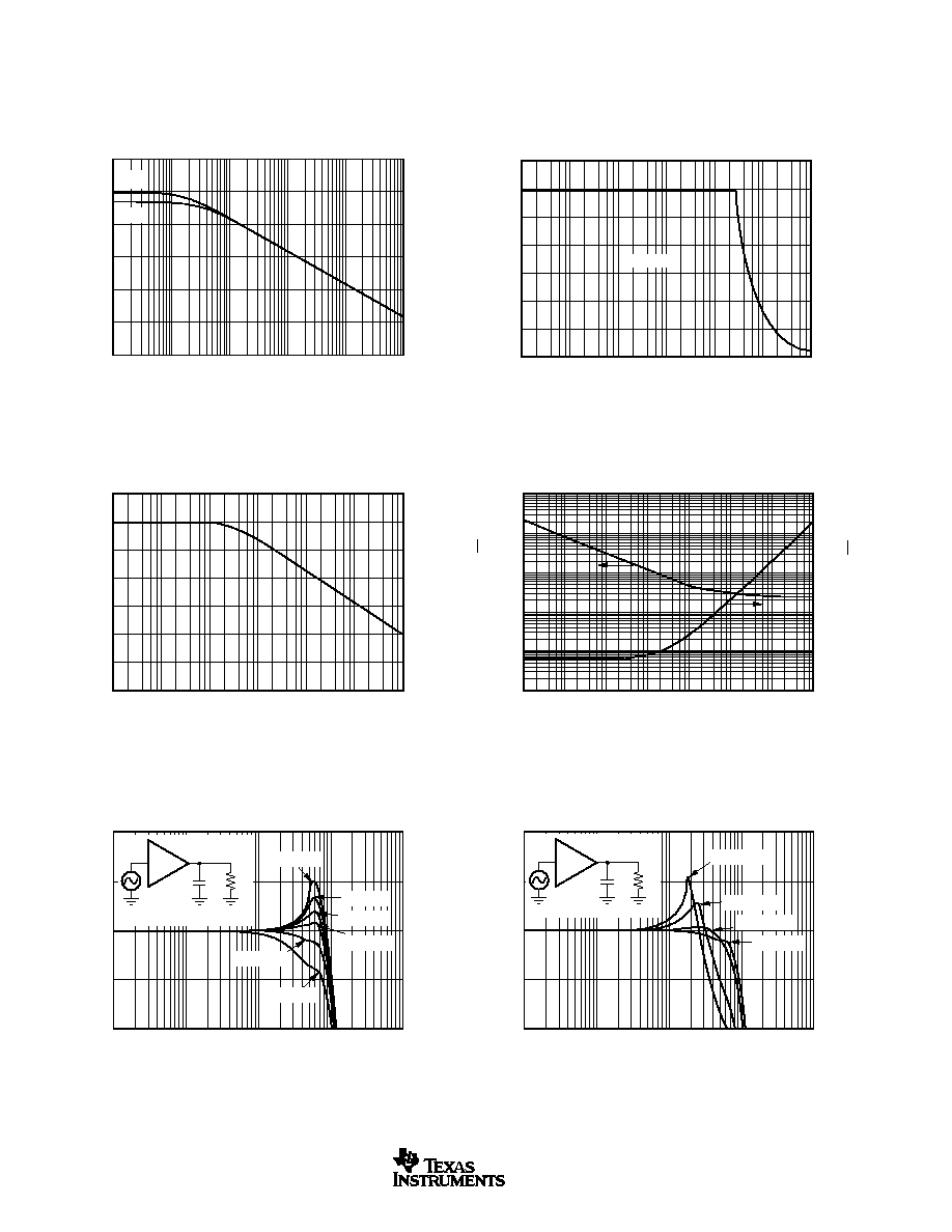
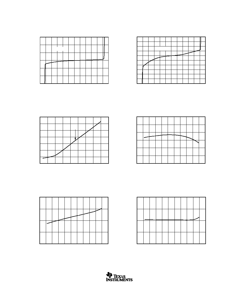
TYPICAL CHARACTERISTICS
At T
A
= +25
∞
C, V
S
=
±
6V, and R
L
= 10k
, unless otherwise noted.
V≠
V+
120
100
80
60
40
20
0
10
100
1k
10k
100k
1M
PSRR vs FREQUENCY
PSRR (dB)
Frequency (Hz)
V
S
=
±
6V
MAXIMUM AMPLITUDE vs FREQUENCY
7
6
5
4
3
2
1
0
Amplitude (V)
10
100
1k
10k
100k
1M
10M
Frequency (Hz)
140
120
100
80
60
40
20
0
CHANNEL SEPARATION vs FREQUENCY
10
100
1k
10k
100k
1M
10M
Channel Separation (dB)
Frequency (Hz)
INPUT CURRENT AND VOLTAGE SPECTRAL
NOISE vs FREQUENCY
10k
1k
100
10
1
0.1
10k
1k
100
10
1
0.1
V
oltage Noise (nV/
Hz)
Frequency (Hz)
0.1
1
10
100
1k
10k
100k
1M
Current Noise (fA/
Hz)
20
10
0
≠10
≠20
10k
100k
1M
10M
100M
GAIN vs FREQUENCY
Gain (dB)
Frequency (Hz)
C
L
R
L
C
L
= 10pF
R
L
= 100
R
L
= 10k
R
L
= 1k
R
L
= 500
R
L
= 350
R
L
= 200
20
10
0
≠10
≠20
10k
100k
1M
10M
100M
GAIN vs FREQUENCY
Gain (dB)
Frequency (Hz)
C
L
= 1000pF
C
L
= 500pF
C
L
= 100pF
C
L
= 10pF
C
L
R
L
R
L
= 200
BUF04701
5
SBOS214B
www.ti.com
TYPICAL CHARACTERISTICS
(Cont.)
At T
A
= +25
∞
C, V
S
=
±
6V, and R
L
= 10k
, unless otherwise noted.
15
10
5
0
≠5
≠10
≠15
≠6
≠5
≠4
≠3
≠2
≠1
0
1
2
3
4
5
6
INPUT BIAS CURRENT (I
B
) vs COMMON-MODE
VOLTAGE (V
CM
) TEMPERATURE = 25∫C
I
B
(pA)
V
CM
(V)
V
S
=
±
5V
INPUT BIAS CURRENT (I
B
) vs COMMON-MODE
VOLTAGE (V
CM
) TEMPERATURE = 85
∞
C
500
400
300
200
100
0
≠100
≠200
≠300
≠400
≠500
≠6
≠5
≠4
≠3
≠2
≠1
0
1
2
3
4
5
6
I
B
(pA)
V
CM
(V)
V
S
=
±
5V
I
B
100k
10k
1k
100
10
1.0
0.1
0.01
≠50
≠25
0
25
50
75
100
125
150
175
Bias Current (pA)
Temperature (
∞
C)
INPUT BIAS (I
B
) AND CURRENT
vs TEMPERATURE
120
110
100
90
80
70
60
≠100 ≠75 ≠50 ≠25
0
25
50
75
100 125 150 175
PSRR vs TEMPERATURE
PSRR (dB)
Temperature (
∞
C)
2.0
1.5
1.0
0.5
0.0
I
Q
per
Amplitude (mA)
QUIESCENT CURRENT vs TEMPERATURE
≠100 ≠75 ≠50 ≠25
0
25
50
75
100 125 150 175
Temperature (
∞
C)
1.005
1.000
0.995
≠100
≠50
0
50
100
150
??
GAIN vs TEMPERATURE
Gain (V/V)
Temperature (
∞
C)