BUF11702, BUF07702: Multi-Channel LCD Gamma Correction Buffer (Rev. F)
SLOS359F - MARCH 2001 - REVISED MAY 2004
MULTI CHANNEL LCD GAMMA CORRECTION BUFFER
BUF11702
BUF07702
FEATURES
D
Gamma Correction Channels: 10, 6
D
Integrated V
COM
Buffer
D
Excellent Output Current Drive:
- Gamma Channels: > 30mA at
0.5V Swing to Rails
(1)
- V
COM
: > 150mA at
5V Swing to Rails
(1)
D
Large Capacitive Load Drive Capability
D
Rail-to-Rail Output
D
PowerPAD Package
D
Low-Power/Channel: < 340
µ
A
D
Wide Supply Range: 4.5V to 16V
D
Specified for 0
°
C to 85
°
C
D
High ESD Rating: 4kV
(1) See typical characteristic curves for detail.
MODEL
GAMMA
CHANNELS
VCOM CHANNELS
BUF11702
10
1
BUF07702(1)
6
1
(1) The BUF07702 is not recommended for new designs. Informa-
tion is provided for reference only. For new designs, the pin-com-
patible BUF07703 is recommended; more information can be
found at www.ti.com.
DESCRIPTION
The BUFxx702 are a series of multi-channel buffers
targeted towards gamma correction in high-resolution
LCD panels. The number of gamma correction
channels required depends on a variety of factors and
differs greatly from design to design. Therefore, various
channel options are offered. For additional space and
cost savings, a V
COM
channel with higher current drive
capability is integrated in the BUF11702 and
BUF07702.
The various buffers within the BUFxx702 are carefully
matched to the voltage I/O requirements for the gamma
correction application. Each buffer is capable of driving
heavy capacitive loads and offers fast load current
switching. The V
COM
channel has increased output
drive of > 100mA and can handle even larger capacitive
loads.
The BUF07702 and BUF11702 is available in the
TSSOP-PowerPAD
package for dramatically
increased power dissipation capability. This way, a
large number of channels can be handled safely in one
package.
A flow-through pinout has been adopted to allow simple
PCB routing and maintain the cost-effectiveness of this
solution. All inputs and outputs of the BUFxx702
incorporate internal ESD protection circuits that prevent
functional failures at voltages up to 4kV (HBM) as
tested under MIL-STD-883C Method 3015.
www.ti.com
Copyright
2001-2004, Texas Instruments Incorporated
Please be aware that an important notice concerning availability, standard warranty, and use in critical applications of Texas Instruments
semiconductor products and disclaimers thereto appears at the end of this data sheet.
PRODUCTION DATA information is current as of publication date. Products
conform to specifications per the terms of Texas Instruments standard warranty.
Production processing does not necessarily include testing of all parameters.
PowerPAD is a trademark of Texas Instruments Incorporated. All other trademarks are the property of their respective owners.
BUF11702
BUF07702
SLOS359F - MARCH 2001 - REVISED MAY 2004
www.ti.com
2
ABSOLUTE MAXIMUM RATINGS
over operating free-air temperature range unless otherwise noted(1)
PARAMETERS
BUFXX702
UNIT
Supply, VDD(2)
16.5
V
Input Voltage Range, VI
VDD
V
Continuous Total Power Dissipation
See Dissipation
Rating Table
Operating Free-Air Temperature Range, TA
0 to 85
°
C
Maximum Junction Temperature, TJ
150
°
C
Storage Temperature Range, TSTG
-65 to 150
°
C
Lead Temperature 1.6mm (1/16 inch) from case for 10s
260
°
C
(1) Stresses beyond those listed under absolute maximum ratings may cause permanent damage to the device. These are stress ratings only, and
functional operation of the device at these or any other conditions beyond those indicated under recommended operating conditions is not
implied. Exposure to absolute-maximum-rated conditions for extended periods may affect device reliability.
(2) All voltage values are with respect to GND.
ORDERING INFORMATION
PRODUCT
PACKAGE-LEAD
PACKAGE
DESIGNATOR(1)
SPECIFIED
TEMPERATURE
RANGE
ORDERING
NUMBER
TRANSPORT MEDIA,
QUANTITY
BUF11702
TSSOP-28
PWP
0
°
C to +85
°
C
BUF11702PWP
Tube, 50
BUF11702
TSSOP-28
PWP
0
°
C to +85
°
C
BUF11702PWPR
Reels, 2000
BUF07702(2)
TSSOP-20
PWP
0
°
C to +85
°
C
BUF07702PWP
Tube, 70
BUF07702(2)
TSSOP-20
PWP
0
°
C to +85
°
C
BUF07702PWPR
Reels, 2000
(1) For the most current specification and package information, refer to the Package Option Addendum at the end of this data sheet.
(2) The BUF07702 is not recommended for new designs. For new designs, the pin-compatible BUF07703 is recommended.
DISSIPATION RATING TABLE
PACKAGE TYPE
PACKAGE
DESIGNATOR
q
JC
(
°
C/W)
q
JA
(1)
(
°
C/W)
TA
25
°
C(2)
POWER RATING
TSSOP-28
PWP (28)
0.72
27.9
3.5 W
TSSOP-20(3)
PWP (20)
1.40
26.1
3.8 W
(1) With 2oz trace and PowerPAD soldered to copper landing pad.
(2) TJ = 125
°
C.
(3) The BUF07702 is not recommended for new designs. For new designs, the pin-compatible BUF07703 is recommended.
RECOMMENDED OPERATING CONDITIONS
MIN
NOM
MAX
UNIT
Supply Voltage, VDD
4.5
16
V
Operating Free-Air Temperature, TA
0
85
°
C
BUF11702
BUF07702
SLOS359F - MARCH 2001 - REVISED MAY 2004
www.ti.com
3
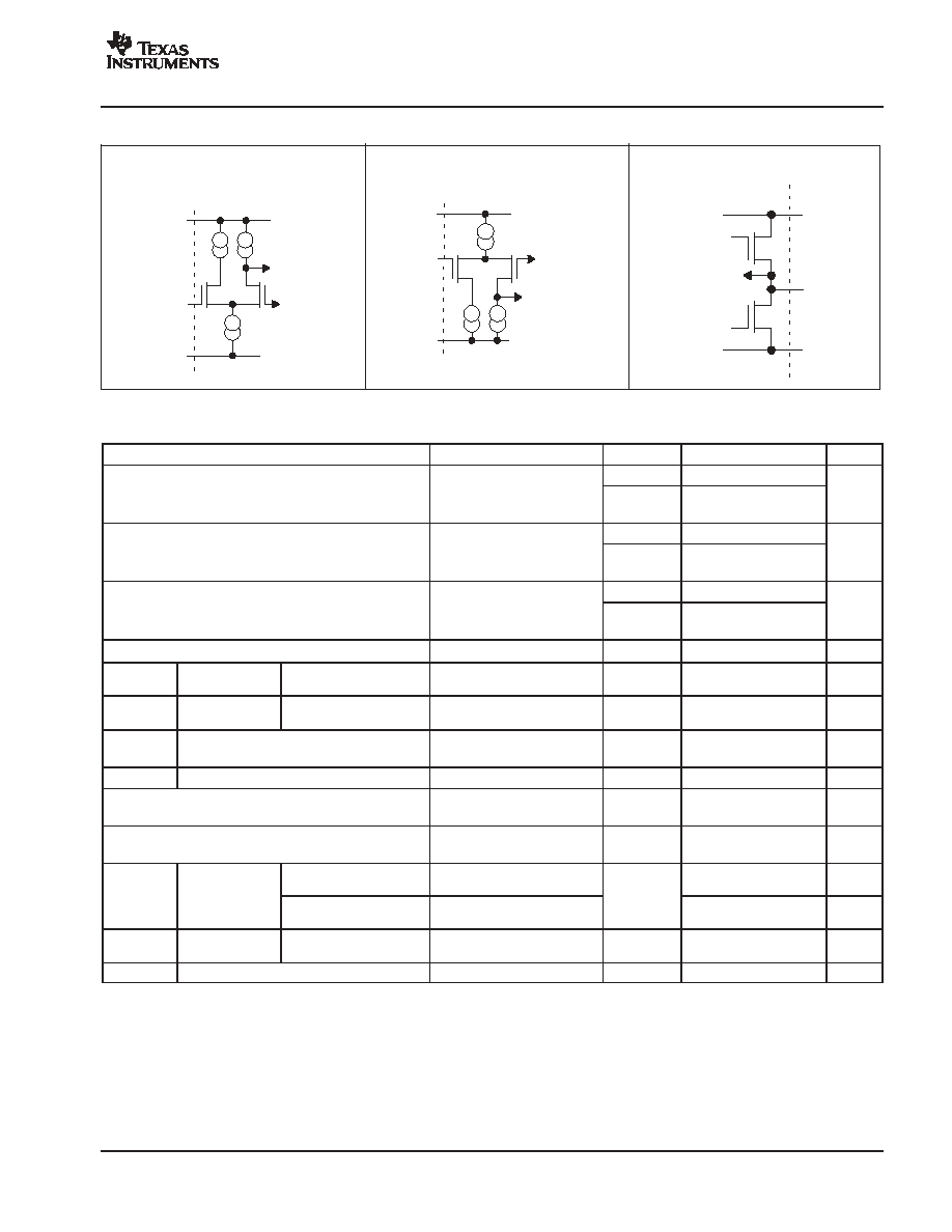
EQUIVALENT SCHEMATICS OF INPUTS AND OUTPUTS
Next
Stage
Buffer
Output
VS
Buffer
Input
GND
Internal to
BUF11702
Buffer
Output
Buffer
Input
VS
Next Stage
GND
Internal to
BUF11702
INPUT STAGE OF BUFFERS
BUF11702: 1 to 5 and VCOM
BUF07702: 1 to 3 and VCOM
INPUT STAGE OF BUFFERS
BUF11702: 6 to 10
BUF07702: 4 to 6
Previous
Stage
VS
Buffer
Output
Previous
Stage
Inverting
Input
GND
OUTPUT STAGE OF ALL BUFFERS
ELECTRICAL CHARACTERISTICS
Over operating free-air temperature range, VDD = 4.5V to 16V, TA = 25
°
C, unless otherwise noted.
PARAMETER
TEST CONDITIONS
TA
MIN
TYP
MAX
UNIT
25
°
C
1.5
12
VIO
Input offset voltage
VI = VDD/2, RS = 50
Full
Range(1)
15
mV
25
°
C
1
IIB
Input bias current
VI = VDD/2
Full
Range(1)
200
pA
25
°
C
62
80
kSVR
Supply voltage rejection ratio (
VDD/
VIO)
VDD = 4.5 V to 16 V
Full
Range(1)
60
dB
Buffer gain
VI = 5 V
25
°
C
0.9995
V/V
BW_3dB
3dB bandwidth
Gamma buffers
VCOM buffer
CL = 100 pF, RL = 2 k
25
°
C
1
0.6
MHz
SR
Slew rate
Gamma buffers
VCOM buffer
CL = 100 pF, RL = 2 k
VIN = 2V to 8V
25
°
C
1
0.7
V/
µ
s
Transient load regulation
IO = 0 to
±
5 mA, VO = 5 V
CL = 100 pF tT = 0.1
µ
s
25
°
C
900
mV
Transient load response
See Figure 2
25
°
C
160
mV
tS (I-sink)
Settling time-current
IO = 0 to -5 mA VO = 5 V
CL = 100 pF RL = 2 k
Full
Range(1)
1
µ
s
tS (I-src)
Settling time-current
IO = 0 to +5 mA VO = 5 V
CL = 100 pF RL = 2 k
Full
Range(1)
2
µ
s
tS
Settling time-
voltage
Gamma buffers
VI = 4.5 V to 5.5 V 0.1%
VI = 5.5 V to 4.5 V 0.1%
25
°
C
6
4.6
µ
s
tS
Settling time-
voltage
VCOM buffer
VI = 4.5 V to 5.5 V 0.1%
VI = 5.5 V to 4.5 V 0.1%
25
°
C
5.8
5.6
µ
s
Vn
Noise voltage
Gamma buffers
VCOM buffer
VI = 5 V f = 1 kHz
25
°
C
45
40
nV/Hz
Crosstalk
VIP-P = 6 V, f = 1 kHz
25
°
C
85
dB
(1) Full Range is 0
°
C to 85
°
C.
BUF11702
BUF07702
SLOS359F - MARCH 2001 - REVISED MAY 2004
www.ti.com
4
ELECTRICAL CHARACTERISTICS: BUF11702
Over operating free-air temperature range, VDD = 4.5V to 16V, TA = 25
°
C, unless otherwise noted.
PARAMETER
TEST CONDITIONS
TA(1)
MIN
TYP
MAX
UNIT
IDD
Supply current
ALL
VO = VDD/2, VI = VDD/2,
25
°
C
2.5
3.7
mA
IDD
Supply current
ALL
VO = VDD/2, VI = VDD/2,
VDD = 10 V
Full Range
5.5
mA
Buffers 1-5
1
VDD
Common-mode input range
Buffers 6-10
25
°
C
0
VDD-1
V
Common-mode input range
VCOM buffer
25 C
1
VDD
V
VCOM buffer sinking
VDD = 10 V,
25
°
C
1
1.2
VCOM buffer sinking
VDD = 10 V,
IO = 1 mA to 30 mA
Full Range
2.5
VCOM buffer sourcing
VDD = 10 V,
25
°
C
1
1.2
Load regulation
VCOM buffer sourcing
VDD = 10 V,
IO = -1 mA to -30 mA
Full Range
2.5
mV/mA
Load regulation
Buffers 1-10 sinking
VDD = 10 V,
25
°
C
0.85
1
mV/mA
Buffers 1-10 sinking
VDD = 10 V,
IO = 1 mA to 10 mA
Full Range
1.5
Buffers 1-10 sourcing
VDD = 10 V,
25
°
C
0.85
1
Buffers 1-10 sourcing
VDD = 10 V,
IO = -1 mA to -10 mA
Full Range
1.5
VOSH1
High-level
saturated output
Buffer 1
VDD = 16V,
V = 16V
IO = -5mA,
25
°
C
15.85
15.9
V
VOSH1
High-level
saturated output
voltage
Buffer 1
VDD = 16V,
VI = 16V
IO = -5mA,
Full range
15.8
V
VOSL10
Low-level
saturated output
Buffer 10
VDD = 16 V,
V = 0 V
IO = 5 mA,
25
°
C
0.1
0.15
V
VOSL10
Low-level
saturated output
voltage
Buffer 10
VDD = 16 V,
VI = 0 V
IO = 5 mA,
Full range
0.2
V
VOH1
Buffer 1
VDD = 10 V,
V = 9.8 V
IO = -10 mA,
25
°
C
9.75
9.8
V
VOH1
Buffer 1
VDD = 10 V,
VI = 9.8 V
IO = -10 mA,
Full range
9.7
V
VOH2/3/4/5
Buffer 2/3/4/5
VDD = 10 V,
V = 9.5 V
IO = -10 mA,
25
°
C
9.45
9.5
V
VOH2/3/4/5
Buffer 2/3/4/5
VDD = 10 V,
VI = 9.5 V
IO = -10 mA,
Full range
9.4
V
VOH6/7/8/9
High-level output
voltage
Buffer 6/7/8/9
VDD = 10 V,
V = 8 V
IO = -10 mA,
25
°
C
7.95
8
V
VOH6/7/8/9
High-level output
voltage
Buffer 6/7/8/9
VDD = 10 V,
VI = 8 V
IO = -10 mA,
Full range
7.9
V
VOH10
Buffer 10
VDD = 10 V,
V = 8 V
IO = -10 mA,
25
°
C
7.95
8
V
VOH10
Buffer 10
VDD = 10 V,
VI = 8 V
IO = -10 mA,
Full range
7.9
V
VOHCOM
VCOM buffer
VDD = 10 V,
V = 8 V
IO = -30 mA,
25
°
C
7.95
8
V
VOHCOM
VCOM buffer
VDD = 10 V,
VI = 8 V
IO = -30 mA,
Full range
7.9
V
VOL1
Buffer 1
VDD = 10 V,
V = 2 V
IO = 10 mA,
25
°
C
2
2.05
V
VOL1
Buffer 1
VDD = 10 V,
VI = 2 V
IO = 10 mA,
Full range
2.1
V
VOL2/3/4/5
Buffer 2/3/4/5
VDD = 10 V,
V = 2 V
IO = 10 mA,
25
°
C
2
2.05
V
VOL2/3/4/5
Buffer 2/3/4/5
VDD = 10 V,
VI = 2 V
IO = 10 mA,
Full range
2.1
V
VOL6/7/8/9
Low-level output
voltage
Buffer 6/7/8/9
VDD = 10 V,
V = 0.5 V
IO = 10 mA,
25
°
C
0.5
0.55
V
VOL6/7/8/9
Low-level output
voltage
Buffer 6/7/8/9
VDD = 10 V,
VI = 0.5 V
IO = 10 mA,
Full range
0.6
V
VOL10
Buffer 10
VDD = 10 V,
V = 0.2 V
IO = 10 mA,
25
°
C
0.2
0.25
V
VOL10
Buffer 10
VDD = 10 V,
VI = 0.2 V
IO = 10 mA,
Full range
0.3
V
VOLCOM
VCOM buffer
VDD = 10 V,
V = 2 V
IO = 30 mA,
25
°
C
2
2.05
V
VOLCOM
VCOM buffer
VDD = 10 V,
VI = 2 V
IO = 30 mA,
Full range
2.1
V
(1) Full Range is 0
°
C to 85
°
C.
BUF11702
BUF07702
SLOS359F - MARCH 2001 - REVISED MAY 2004
www.ti.com
5
ELECTRICAL CHARACTERISTICS: BUF07702
Over operating free-air temperature range, VDD = 4.5V to 16V, TA = 25
°
C, unless otherwise noted.
PARAMETER
TEST CONDITIONS
TA(1)
MIN
TYP
MAX
UNIT
IDD
Supply current
ALL
VO = VDD/2, VI = VDD/2
25
°
C
2.5
3.7
mA
IDD
Supply current
ALL
VO = VDD/2, VI = VDD/2
VDD= 10V
Full Range
5.5
mA
Buffers 1-3
1
VDD
Common-mode input range
Buffers 4-6
25
°
C
0
VDD-1
V
Common-mode input range
VCOM buffer
25 C
1
VDD
V
VCOM buffer sinking
VDD = 10 V,
25
°
C
1
1.2
VCOM buffer sinking
VDD = 10 V,
IO = 1 mA to 30 mA
Full Range
2.5
VCOM buffer sourcing
VDD = 10 V,
25
°
C
1
1.2
Load regulation
VCOM buffer sourcing
VDD = 10 V,
IO = -1 mA to -30 mA
Full Range
2.5
mV/mA
Load regulation
Buffers 1-6 sinking
VDD = 10 V,
25
°
C
0.85
1
mV/mA
Buffers 1-6 sinking
VDD = 10 V,
IO = 1 mA to 10 mA
Full Range
1.5
Buffers 1-6 sourcing
VDD = 10 V,
25
°
C
0.85
1
Buffers 1-6 sourcing
VDD = 10 V,
IO = -1 mA to -10 mA
Full Range
1.5
VOSH1
High-level
saturated output
Buffer 1
VDD = 16 V,
V = 16 V
IO = -5 mA,
25
°
C
15.85
15.9
V
VOSH1
High-level
saturated output
voltage
Buffer 1
VDD = 16 V,
VI = 16 V
IO = -5 mA,
Full range
15.8
V
VOSL6
Low-level
saturated output
Buffer 6
VDD = 16 V,
V = 0 V
IO = 5 mA,
25
°
C
0.1
0.15
V
VOSL6
Low-level
saturated output
voltage
Buffer 6
VDD = 16 V,
VI = 0 V
IO = 5 mA,
Full range
0.2
V
VOH1
Buffer 1
VDD = 10 V,
V = 9.8 V
IO = -10 mA,
25
°
C
9.75
9.8
V
VOH1
Buffer 1
VDD = 10 V,
VI = 9.8 V
IO = -10 mA,
Full range
9.7
V
VOH2/3
Buffer 2/3
VDD = 10 V,
V = 9.5 V
IO = -10 mA,
25
°
C
9.45
9.5
V
VOH2/3
Buffer 2/3
VDD = 10 V,
VI = 9.5 V
IO = -10 mA,
Full range
9.4
V
VOH4/5
High-level output
voltage
Buffer 4/5
VDD = 10 V,
V = 8 V
IO = -10 mA,
25
°
C
7.95
8
V
VOH4/5
High-level output
voltage
Buffer 4/5
VDD = 10 V,
VI = 8 V
IO = -10 mA,
Full range
7.9
V
VOH6
Buffer 6
VDD = 10 V,
V = 8 V
IO = -10 mA,
25
°
C
7.95
8
V
VOH6
Buffer 6
VDD = 10 V,
VI = 8 V
IO = -10 mA,
Full range
7.9
V
VOHCOM
VCOM buffer
VDD = 10 V,
V = 8 V
IO = -30 mA,
25
°
C
7.95
8
V
VOHCOM
VCOM buffer
VDD = 10 V,
VI = 8 V
IO = -30 mA,
Full range
7.9
V
VOL1
Buffer 1
VDD = 10 V,
V = 2 V
IO = 10 mA,
25
°
C
2
2.05
V
VOL1
Buffer 1
VDD = 10 V,
VI = 2 V
IO = 10 mA,
Full range
2.1
V
VOL2/3
Buffer 2/3
VDD = 10 V,
V = 2 V
IO = 10 mA,
25
°
C
2
2.05
V
VOL2/3
Buffer 2/3
VDD = 10 V,
VI = 2 V
IO = 10 mA,
Full range
2.1
V
VOL4/5
Low-level output
voltage
Buffer 4/5
VDD = 10 V,
V = 0.5 V
IO = 10 mA,
25
°
C
0.5
0.55
V
VOL4/5
Low-level output
voltage
Buffer 4/5
VDD = 10 V,
VI = 0.5 V
IO = 10 mA,
Full range
0.6
V
VOL6
Buffer 6
VDD = 10 V,
V = 0.2 V
IO = 10 mA,
25
°
C
0.2
0.25
V
VOL6
Buffer 6
VDD = 10 V,
VI = 0.2 V
IO = 10 mA,
Full range
0.3
V
VOLCOM
VCOM buffer
VDD = 10 V,
V = 2 V
IO = 30 mA,
25
°
C
2
2.05
V
VOLCOM
VCOM buffer
VDD = 10 V,
VI = 2 V
IO = 30 mA,
Full range
2.1
V
(1) Full Range is 0
°
C to 85
°
C.
Document Outline
- FEATURES
- DESCRIPTION
- ABSOLUTE MAXIMUM RATINGS
- ORDERING INFORMATION
- DISSIPATION RATING TABLE
- RECOMMENDED OPERATING CONDITIONS
- EQUIVALENT SCHEMATICS OF INPUTS AND OUTPUTS
- ELECTRICAL CHARACTERISTICS
- ELECTRICAL CHARACTERISTICS: BUF11702
- ELECTRICAL CHARACTERISTICS: BUF07702
- BUF11702 Pin Configuration
- BUF07702 Pin Configuration
- PARAMETER MEASUREMENT INFORMATION
- TYPICAL CHARACTERISTICS
- DC CURVES
- AC CURVES
- TRANSIENT CURVES
- APPLICATION INFORMATION
- INPUT VOLTAGE RANGE GAMMA BUFFERS
- OUTPUT VOLTAGE SWING GAMMA BUFFERS
- COMMON BUFFER ( VCOM)
- CAPACITIVE LOAD DRIVE
- APPLICATIONS WITH >10 GAMMA CHANNELS
- MULTIPLE VCOM CHANNELS
- COMPLETE LCD SOLUTION FROM TI
- AUDIO POWER AMPLIFIER FOR TV SPEAKERS
- GENERAL POWERPAD DESIGN CONSIDERATIONS
- PowerPAD ASSEMBLY PROCESS
- APPLICATION INFORMATION BUF11702 Demonstration Board
- REFERENCE VOLTAGES