 | –≠–ª–µ–∫—Ç—Ä–æ–Ω–Ω—ã–π –∫–æ–º–ø–æ–Ω–µ–Ω—Ç: BUF602IDR | –°–∫–∞—á–∞—Ç—å:  PDF PDF  ZIP ZIP |
Burr Brown Products
from Texas Instruments
FEATURES
DESCRIPTION
APPLICATIONS
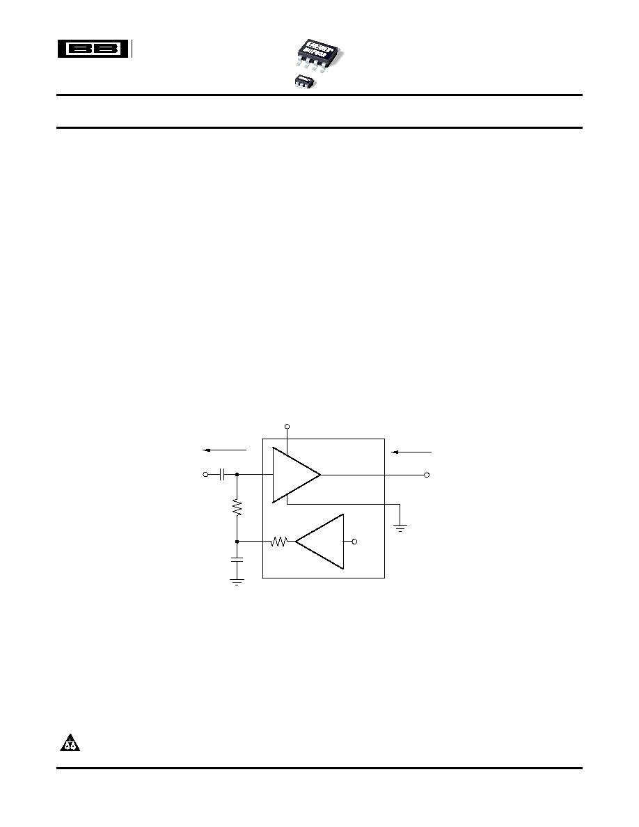
Self-Referenced, AC-Coupled, Single-Supply Buffer
x1
+V
CC
x1
2k
V
OUT
V
IN
2k
Input Z
Z
O
< 2
to 20MHz
V
CC
/2
1
µ
F
200
BUF602
SBOS339 ≠ OCTOBER 2005
High-Speed, Closed-Loop Buffer
∑
Wide Bandwidth: 1000MHz
The BUF602 is a closed-loop buffer recommended for
a wide range of applications. Its wide bandwidth
∑
High Slew Rate: 8000V/
µ
s
(1000MHz) and high slew rate (8000V/
µ
s) make it
∑
Flexible Supply Range:
ideal for buffering very high-frequency signals. For
±
1.4V to
±
6.3V Dual Supplies
AC-coupled
applications,
an
optional
mid-point
+2.8V to +12.6V Single Supply
reference (V
REF
) is provided, reducing the number of
∑
Output Current: 60mA (continuous)
external components required and the necessary
supply current to provide that reference.
∑
Peak Output Current: 350mA
∑
Low Quiescent Current: 5.8mA
The BUF602 is available in a standard SO-8
surface-mount package and in an SOT23-5 where a
∑
Standard Buffer Pinout
smaller footprint is needed.
∑
Optional Mid-Supply Reference Buffer
∑
Low Impedance Reference Buffers
∑
Clock Distribution Circuits
∑
Video/Broadcast Equipment
∑
Communications Equipment
∑
High-Speed Data Acquisition
∑
Test Equipment and Instrumentation
Please be aware that an important notice concerning availability, standard warranty, and use in critical applications of Texas
Instruments semiconductor products and disclaimers thereto appears at the end of this data sheet.
All trademarks are the property of their respective owners.
PRODUCTION DATA information is current as of publication date.
Copyright © 2005, Texas Instruments Incorporated
Products conform to specifications per the terms of the Texas
Instruments standard warranty. Production processing does not
necessarily include testing of all parameters.
www.ti.com
ABSOLUTE MAXIMUM RATINGS
(1)
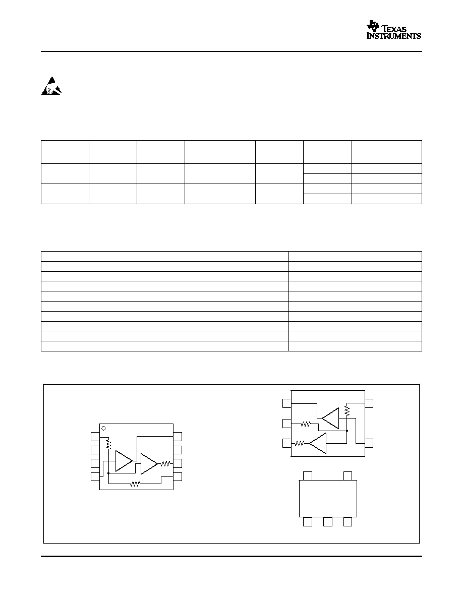
Top View
1
2
3
5
4
Out
-
V
CC
V
REF
+V
CC
In
AWO
1
2
3
5
4
Pin Orientation/Package Marking
SOT23-5
x1
x1
200
50k
50k
1
2
3
4
8
7
6
5
+V
CC
NC
NC
In
Out
NC
V
REF
-
V
CC
SO-8
NC = No Connection
x1
x1
200
50k
50k
BUF602
SBOS339 ≠ OCTOBER 2005
This integrated circuit can be damaged by ESD. Texas Instruments recommends that all integrated
circuits be handled with appropriate precautions. Failure to observe proper handling and installation
procedures can cause damage.
ESD damage can range from subtle performance degradation to complete device failure. Precision
integrated circuits may be more susceptible to damage because very small parametric changes could
cause the device not to meet its published specifications.
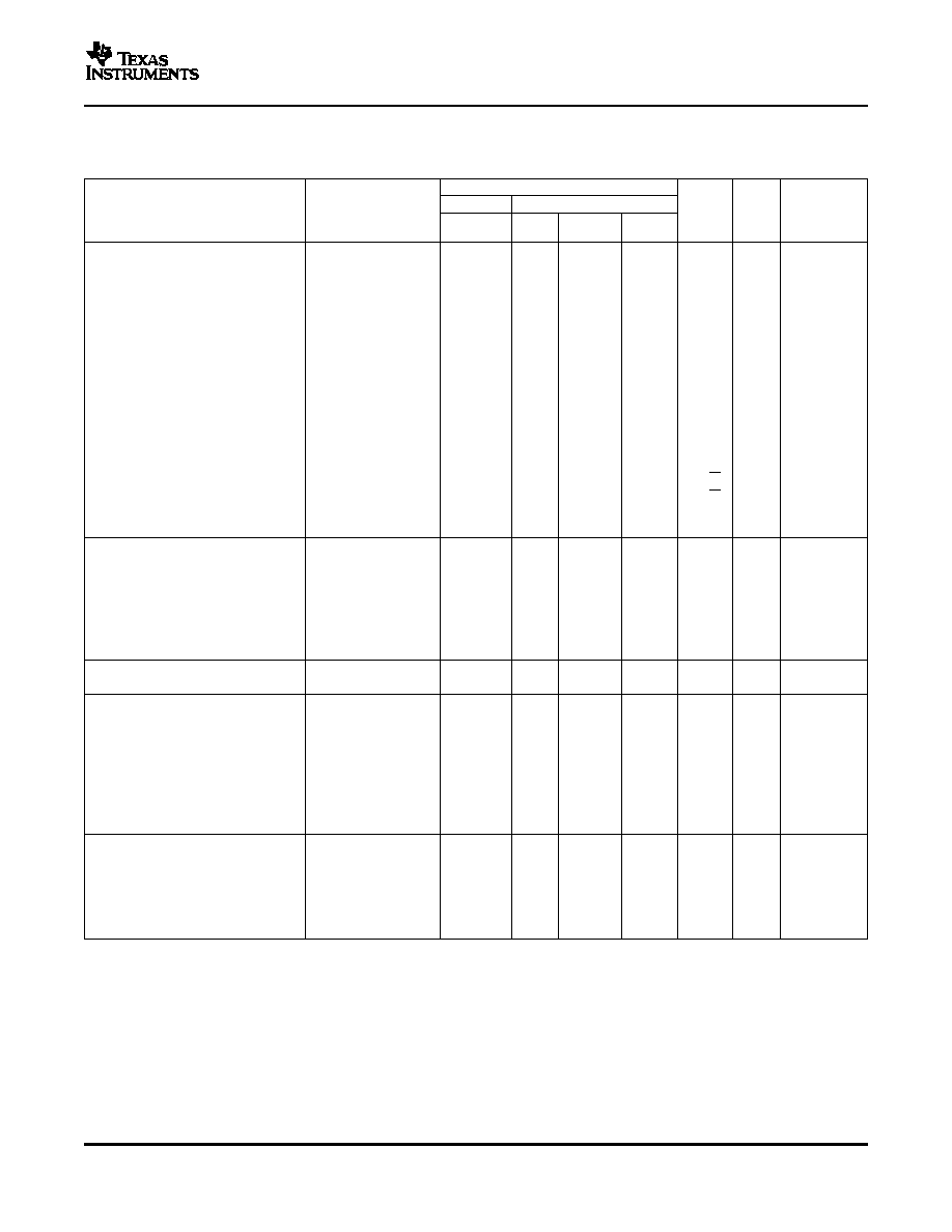
ORDERING INFORMATION
(1)
SPECIFIED
PACKAGE
TEMPERATURE
PACKAGE
ORDERING
TRANSPORT MEDIA,
PRODUCT
PACKAGE
DESIGNATOR
RANGE
MARKING
NUMBER
QUANTITY
BUF602ID
Rails, 75
BUF602
SO-8
D
≠45
∞
C to +85
∞
C
BUF602
BUF602IDR
Tape and Reel, 2500
BUF602IDBVT
Tape and Reel, 250
BUF602
SOT23-5
DBV
≠45
∞
C to +85
∞
C
AWO
BUF602IDBVR
Tape and Reel, 3000
(1)
For the most current package and ordering information, see the Package Option Addendum at the end of this document or see the TI
web site at
www.ti.com
.
Power Supply
±
6.5V
DC
Internal Power Dissipation
See Thermal Information
Input Common-Mode Voltage Range
±
V
S
Storage Temperature Range: D, DBV
≠40
∞
C to +125
∞
C
Lead Temperature (soldering, 10s)
+300
∞
C
Junction Temperature (T
J
)
+150
∞
C
ESD Rating:
Human Body Model (HBM)
2000V
Charge Device Model (CDM)
1000V
Machine Model (MM)
200V
(1)
Stresses above these ratings may cause permanent damage. Exposure to absolute maximum conditions for extended periods may
degrade device reliability. These are stress ratings only, and functional operation of the device at these or any other conditions beyond
those specified is not supported.
2
www.ti.com
ELECTRICAL CHARACTERISTICS: V
S
=
±
5V
BUF602
SBOS339 ≠ OCTOBER 2005
Boldface limits are tested at +25
∞
C.
At R
L
= 100
, unless otherwise noted.
BUF602ID, IDBV
TYP
MIN/MAX OVER TEMPERATURE
0
∞
C to
≠40
∞
C to
MIN/
PARAMETER
CONDITIONS
+25
∞
C
+25
∞
C
(2)
70
∞
C
(3)
+85
∞
C
(3)
UNITS
MAX
TEST LEVEL
(1)
AC PERFORMANCE
(See figure 30)
Bandwidth
V
O
= 500mV
PP
1000
560
550
540
MHz
min
B
V
O
= 1V
PP
920
MHz
typ
C
Full Power Bandwidth
V
O
= 5V
PP
880
MHz
typ
C
Bandwidth for 0.1dB Flatness
V
O
= 500mV
PP
240
MHz
typ
C
Slew Rate
V
O
= 5V Step
8000
7000
6000
5000
V/
µ
s
min
B
Rise Time and Fall Time
V
O
= 0.2V Step
350
625
640
650
ps
max
B
Settling Time to 0.05%
V
O
= 1V Step
6
ns
typ
C
Harmonic Distortion
V
O
= 2V
PP
, 5MHz
2nd-Harmonic
R
L
= 100
≠57
≠44
≠44
≠42
dBc
max
B
R
L
= 500
≠76
≠63
≠62
≠60
dBc
max
B
3rd-Harmonic
R
L
= 100
≠68
≠63
≠63
≠63
dBc
max
B
R
L
= 500
≠98
≠85
≠84
≠82
dBc
max
B
Input Voltage Noise
f > 100kHz
4.8
5.1
5.6
6.0
nV/
Hz
max
B
Input Current Noise
f > 100kHz
2.1
2.6
2.7
2.8
pA/
Hz
max
B
Differential Gain
NTSC, R
L
= 150
to 0V
0.15
%
typ
C
Differential Phase
NTSC, R
L
= 150
to 0V
0.04
∞
typ
C
BUFFER DC PERFORMANCE
(4)
Maximum Gain
R
L
= 500
0.99
1
1
1
V/V
max
A
Minimum Gain
R
L
= 500
0.99
0.98
0.98
0.98
V/V
min
A
Input Offset Voltage
±
16
±
30
±
36
±
38
mV
max
A
Average Input Offset Voltage Drift
±
125
±
125
µ
V/
∞
C
max
B
Input Bias Current
±
3
±
7
±
8
±
8.5
µ
A
max
A
Average Input Bias Current Drift
±
20
±
20
nA/
∞
C
max
B
BUFFER INPUT
Input Impedance
1.0 || 2.1
M
|| pF
typ
C
BUFFER OUTPUT
Output Voltage Swing
R
L
= 100
±
3.8
±
3.7
±
3.7
±
3.7
V
min
B
R
L
= 500
±
4.0
±
3.8
±
3.8
±
3.8
V
min
A
Output Current (Continuous)
V
O
= 0V
±
60
±
50
±
49
±
48
mA
min
A
Peak Output Current
V
O
= 0V
±
350
mA
typ
C
Closed-Loop Output Impedance
f
10MHz
1.4
typ
C
POWER SUPPLY
Specified Operating Voltage
±
5
V
typ
C
Maximum Operating Voltage
±
6.3
±
6.3
±
6.3
V
max
A
Minimum Operating Voltage
±
1.4
±
1.4
±
1.4
V
min
B
Maximum Quiescent Current
V
S
=
±
5V
5.8
6.3
6.9
7.2
mA
max
A
Minimum Quiescent Current
V
S
=
±
5V
5.8
5.3
4.9
4.3
mA
min
A
Power-Supply Rejection Ratio (+PSRR)
54
48
46
45
dB
min
A
(1)
Test levels: (A) 100% tested at 25
∞
C. Over temperature limits set by characterization and simulation. (B) Limits set by characterization
and simulation. ©) Typical value only for information.
(2)
Junction temperature = ambient for 25
∞
C specifications.
(3)
Junction temperature = ambient at low temperature limit; junction temperature = ambient + 8
∞
C at high temperature limit for over
temperature specifications.
(4)
Current is considered positive out of node.
3
www.ti.com
BUF602
SBOS339 ≠ OCTOBER 2005
ELECTRICAL CHARACTERISTICS: V
S
=
±
5V (continued)
Boldface limits are tested at +25
∞
C.
At R
L
= 100
, unless otherwise noted.
BUF602ID, IDBV
TYP
MIN/MAX OVER TEMPERATURE
0
∞
C to
≠40
∞
C to
MIN/
PARAMETER
CONDITIONS
+25
∞
C
+25
∞
C
(2)
70
∞
C
(3)
+85
∞
C
(3)
UNITS
MAX
TEST LEVEL
(1)
THERMAL CHARACTERISTICS
Specification: ID
≠40 to +85
∞
C
typ
C
Thermal Resistance
JA
D
SO-8
Junction-to-Ambient
125
∞
C/W
typ
C
DBV
SOT23-5
Junction-to-Ambient
150
∞
C/W
typ
C
4
www.ti.com
ELECTRICAL CHARACTERISTICS: V
S
= +5V
BUF602
SBOS339 ≠ OCTOBER 2005
Boldface limits are tested at +25
∞
C.
At R
L
= 100
to V
S
/2, unless otherwise noted.
BUF602ID, IDBV
TYP
MIN/MAX OVER TEMPERATURE
0
∞
C to
≠40
∞
C to
MIN/
PARAMETER
CONDITIONS
+25
∞
C
+25
∞
C
(2)
70
∞
C
(3)
+85
∞
C
(3)
UNITS
MAX
TEST LEVEL
(1)
AC PERFORMANCE
(See figure 31)
Bandwidth
V
O
= 500mV
PP
780
400
400
390
MHz
min
B
V
O
= 1V
PP
700
MHz
typ
C
Full-Power Bandwidth
V
O
= 3V
PP
420
MHz
typ
C
Bandwidth for 0.1dB Flatness
V
O
= 500mV
PP
130
MHz
typ
C
Slew Rate
V
O
= 3V Step
2500
1800
1600
1400
V/
µ
s
min
B
Rise Time and Fall Time
V
O
= 0.2V Step
450
875
875
900
ps
max
B
Settling Time to 0.05%
V
O
= 1V Step
6
ns
typ
C
Harmonic Distortion
V
O
= 2V
PP
, 5MHz
2nd-Harmonic
R
L
= 100
≠50
≠45
≠44
≠43
dBc
max
B
R
L
= 500
≠73
≠62
≠61
≠60
dBc
max
B
3rd-Harmonic
R
L
= 100
≠70
≠64
≠64
≠63
dBc
max
B
R
L
= 500
≠73
≠72
≠72
≠71
dBc
max
B
Input Voltage Noise
f > 100kHz
4.9
5.2
5.7
6.1
nV/
Hz
max
B
Input Current Noise
f > 100kHz
2.2
2.7
2.8
2.9
pA/
Hz
max
B
Differential Gain
NTSC, R
L
= 100
to V
S
/2
0.16
%
typ
C
Differential Phase
NTSC, R
L
= 100
to V
S
/2
0.05
∞
typ
C
BUFFER DC PERFORMANCE
(4)
Maximum Gain
R
L
= 500
0.99
1
1
1
V/V
max
A
Minimum Gain
R
L
= 500
0.99
0.98
0.98
0.98
V/V
min
A
Input Offset Voltage
±
16
±
30
±
36
±
38
mV
max
A
Average Input Offset Voltage Drift
±
125
±
125
µ
V/
∞
C
max
B
Input Bias Current
±
3
±
7
±
8
±
8.5
µ
A
max
A
Average Input Bias Current Drift
±
20
±
20
nA/
∞
C
max
B
BUFFER INPUT
Input Impedance
1.0 || 2.1
M
|| pF
typ
C
BUFFER OUTPUT
Most Positive Output Voltage
R
L
= 100
+3.9
+3.7
+3.7
+3.7
V
min
B
R
L
= 500
+4.1
+3.8
+3.8
+3.8
V
min
A
Least Positive Output Voltage
R
L
= 100
+1.1
+1.3
+1.3
+1.3
V
max
B
R
L
= 500
+0.9
+1.2
+1.2
+1.2
V
max
A
Output Current (Continuous)
V
O
= 0V
±
60
±
50
±
49
±
48
mA
min
A
Peak Output Current
V
O
= 0V
±
160
mA
typ
C
Closed-Loop Output Impedance
f
10MHz
1.4
typ
C
MID-POINT REFERENCE OUTPUT
Maximum Mid Supply Reference Voltage
2.5
2.6
2.6
2.6
V
max
A
Minimum Mid Supply Reference Voltage
2.5
2.4
2.4
2.4
V
min
A
Mid-Supply Output Current, Sourcing
800
µ
A
typ
C
Mid-Supply Output Current, Sinking
70
µ
A
typ
C
Mid-Supply Output Impedance
200
typ
C
(1)
Test levels: (A) 100% tested at 25
∞
C. Over temperature limits set by characterization and simulation. (B) Limits set by characterization
and simulation. ©) Typical value only for information.
(2)
Junction temperature = ambient for 25
∞
C specifications.
(3)
Junction temperature = ambient at low temperature limit; junction temperature = ambient + 4
∞
C at high temperature limit for over
temperature specifications.
(4)
Current is considered positive out of node.
5