
TPS60400, TPS60401, TPS60402, TPS60403
UNREGULATED 60-mA CHARGE PUMP VOLTAGE INVERTER
SLVS324 ≠ JULY 2001
1
POST OFFICE BOX 655303
∑
DALLAS, TEXAS 75265
features
D
Inverts Input Supply Voltage
D
Up to 60-mA Output Current
D
Only Three Small 1-
µ
F Ceramic Capacitors
Needed
D
Input Voltage Range From 1.6 V to 5.5 V
D
PowerSave-Mode for Improved Efficiency
at Low Output Currents (TPS60400)
D
Device Quiescent Current Typical 100
µ
A
D
Integrated Active Schottky-Diode for
Start-Up Into Load
D
Small 5-Pin SOT23 Package
D
Evaluation Module Available
TPS60400EVM≠178
applications
D
LCD Bias
D
GaAs Bias for RF Power Amps
D
Sensor Supply in Portable Instruments
D
Bipolar Amplifier Supply
D
Medical Instruments
D
Battery-Operated Equipment
description
The TPS6040x is a family of devices that generate an unregulated negative output voltage from an input voltage
ranging from 1.6 V to 5.5 V. The devices are typically supplied by a preregulated supply rail of 5 V or 3.3 V. Due
to its wide input voltage range, two or three NiCd, NiMH, or alkaline battery cells, as well as one Li-Ion cell can
also power them.
Only three external 1-
µ
F capacitors are required to build a complete dc/dc charge pump inverter. Assembled
in a 5-pin SOT23 package, the complete converter can be built on a 50 mm
2
board area. Additional board area
and component count reduction is achieved by replacing the Schottky diode that is typically needed for start-up
into load by integrated circuitry.
The TPS6040x can deliver a maximum output current of 60 mA with a typical conversion efficiency of greater
than 90% over a wide output current range. Three device options with 20-kHz, 50-kHz, and 250-kHz fixed
frequency operation are available. One device comes with a variable switching frequency to reduce operating
current in applications with a wide load range and enables the design with low-value capacitors.
typical application circuit
TPS60400
CFLY≠
CFLY+
3
5
OUT
IN
GND
1
2
4
CI
1
µ
F
CO
1
µ
F
Output
≠1.6 V to ≠5 V,
Max 60 mA
Input
1.6 V to 5.5 V
C(fly)
1
µ
F
≠5
≠4
≠3
≠2
≠1
0
0
1
2
3
4
5
IO = 60 mA
IO = 30 mA
IO = 1 mA
TA = 25
∞
C
VI ≠ Input Voltage ≠ V
≠ Output V
oltage ≠ V
TPS60400
OUTPUT VOLTAGE
vs
INPUT VOLTAGE
V
O
Copyright
2001, Texas Instruments Incorporated
Please be aware that an important notice concerning availability, standard warranty, and use in critical applications of
Texas Instruments semiconductor products and disclaimers thereto appears at the end of this data sheet.
3
2
4
5
DBV PACKAGE
(TOP VIEW)
1
OUT
IN
CFLY≠
CFLY+
GND
PRODUCTION DATA information is current as of publication date.
Products conform to specifications per the terms of Texas Instruments
standard warranty. Production processing does not necessarily include
testing of all parameters.
TPS60400, TPS60401, TPS60402, TPS60403
UNREGULATED 60-mA CHARGE PUMP VOLTAGE INVERTER
SLVS324 ≠ JULY 2001
2
POST OFFICE BOX 655303
∑
DALLAS, TEXAS 75265
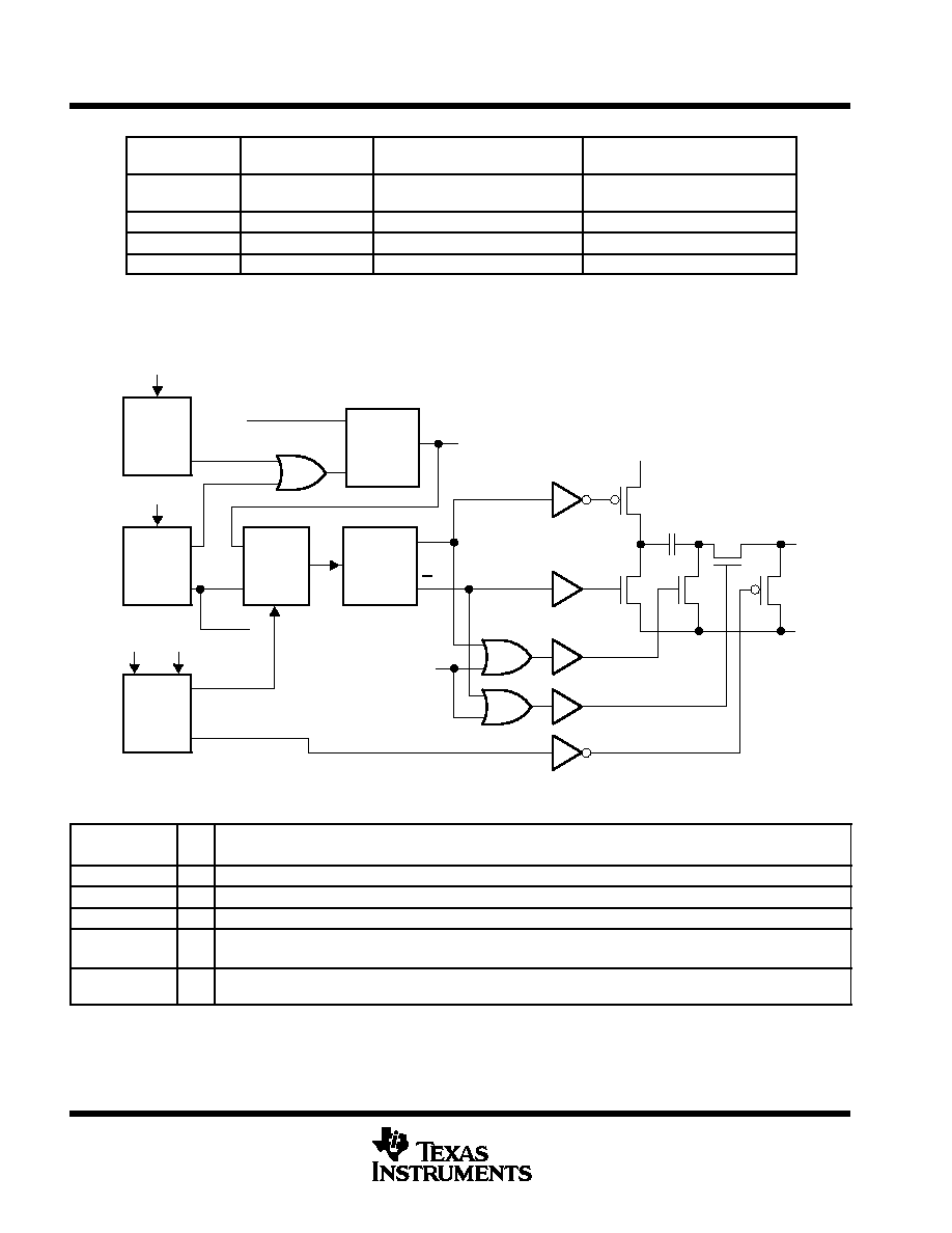
AVAILABLE OPTIONS
PART NUMBER
MARKING DBV
PACKAGE
TYPICAL FLYING CAPACITOR
[
µ
F]
FEATURE
TPS60400DBV
PFKI
1
Variable switching frequency
50 kHz≠250 kHz
TPS60401DBV
PFLI
10
Fixed frequency 20 kHz
TPS60402DBV
PFMI
3.3
Fixed frequency 50 kHz
TPS60403DBV
PFNI
1
Fixed frequency 250 kHz
The DBV package is available taped and reeled. Add R suffix to device type (e.g. TPS60400DBVR) to order quantities of
3000 devices per reel. Add T suffix to device type (e.g. TPS60400DBVT) to order quantities of 250 devices per reel.
TPS60400 functional block diagram
Start
FF
R
S
Q
VI ≠ VCFLY+ < 0.5 V
VI
MEAS
VI < 1 V
VI
VO > Vbe
VO
MEAS
VO
OSC
OSC
CHG
50 kHz
VO > ≠1 V
VI / VO
MEAS
VI
VO
VCO_CONT
VO < ≠VI ≠ Vbe
Phase
Generator
DC_ Startup
C(fly)
+
Q3
Q2
Q1
Q4
VI
VO
GND
Q5
Q
Q
B
DC_ Startup
Terminal Functions
TERMINAL
I/O
DESCRIPTION
NAME
NO.
I/O
DESCRIPTION
CFLY+
5
Positive terminal of the flying capacitor C(fly)
CFLY≠
3
Negative terminal of the flying capacitor C(fly)
GND
4
Ground
IN
2
I
Supply input. Connect to an input supply in the 1.6-V to 5.5-V range. Bypass IN to GND with a capacitor that has the
same value as the flying capacitor.
OUT
1
O
Power output with VO = ≠VI
Bypass OUT to GND with the output filter capacitor CO.

TPS60400, TPS60401, TPS60402, TPS60403
UNREGULATED 60-mA CHARGE PUMP VOLTAGE INVERTER
SLVS324 ≠ JULY 2001
3
POST OFFICE BOX 655303
∑
DALLAS, TEXAS 75265
detailed description
operating principle
The TPS60400, TPS60401 charge pumps invert the voltage applied to their input. For the highest performance,
use low equivalent series resistance (ESR) capacitors (e.g., ceramic). During the first half-cycle, switches S2
and S4 open, switches S1 and S3 close, and capacitor (C
(fly)
) charges to the voltage at V
I
. During the second
half-cycle, S1 and S3 open, S2 and S4 close. This connects the positive terminal of C
(fly)
to GND and the
negative to V
O.
By connecting C
(fly)
in parallel, C
O
is charged negative. The actual voltage at the output is more
positive than ≠V
I
, since switches S1≠S4 have resistance and the load drains charge from C
O
.
C(fly)
1
µ
F
S2
S1
S3
S4
CO
1
µ
F
VO (≠VI)
GND
VI
GND
Figure 1. Operating Principle
charge-pump output resistance
The TPS6040x devices are not voltage regulators. The charge pumps output source resistance is
approximately 15
at room temperature (with V
I
= 5 V), and V
O
approaches ≠5 V when lightly loaded. V
O
will
droop toward GND as load current increases.
V
O
= ≠(V
I
≠ R
O
◊
I
O
)
R
O
[
1
osc
C
(fly)
)
4 2R
SWITCH
)
ESR
CFLY
)
ESR
CO
R
O
= output resistance of the converter
efficiency considerations
The power efficiency of a switched-capacitor voltage converter is affected by three factors: the internal losses
in the converter IC, the resistive losses of the capacitors, and the conversion losses during charge transfer
between the capacitors. The internal losses are associated with the IC's internal functions, such as driving the
switches, oscillator, etc. These losses are affected by operating conditions such as input voltage, temperature,
and frequency. The next two losses are associated with the voltage converter circuit's output resistance. Switch
losses occur because of the on-resistance of the MOSFET switches in the IC. Charge-pump capacitor losses
occur because of their ESR. The relationship between these losses and the output resistance is as follows:
P
CAPACITOR LOSSES
+ P
CONVERSION LOSSES
= I
O
2
◊
R
O
R
SWITCH
= resistance of a single MOSFET-switch inside the converter
f
OSC
= oscillator frequency
The first term is the effective resistance from an ideal switched-capacitor circuit. Conversion losses occur during
the charge transfer between C
(fly)
and C
O
when there is a voltage difference between them. The power loss is:
P
CONV.LOSS
+
1
2
C
(fly)
V
2
I
*
V
2
O
)
1
2
C
O
V
2
RIPPLE
*
2V
O
V
RIPPLE
osc
(1)
(2)

TPS60400, TPS60401, TPS60402, TPS60403
UNREGULATED 60-mA CHARGE PUMP VOLTAGE INVERTER
SLVS324 ≠ JULY 2001
4
POST OFFICE BOX 655303
∑
DALLAS, TEXAS 75265
efficiency considerations (continued)
The efficiency of the TPS6040x devices is dominated by their quiescent supply current at low output current and
by their output impedance at higher current.
h ^
I
O
I
O
)
I
Q
1
*
I
O
R
O
V
I
Where, I
Q
= quiescent current.
capacitor selection
To maintain the lowest output resistance, use capacitors with low ESR (see Table 1). The charge-pump output
resistance is a function of C
(fly)
's and C
O
's ESR. Therefore, minimizing the charge-pump capacitor's ESR
minimizes the total output resistance. The capacitor values are closely linked to the required output current and
the output noise and ripple requirements. It is possible to only use 1-
µ
F capacitors of the same type.
input capacitor (C
I
)
Bypass the incoming supply to reduce its ac impedance and the impact of the TPS6040x switching noise. The
recommended bypassing depends on the circuit configuration and where the load is connected. When the
inverter is loaded from OUT to GND, current from the supply switches between 2 x I
O
and zero. Therefore, use
a large bypass capacitor (e.g., equal to the value of C
(fly)
) if the supply has high ac impedance. When the inverter
is loaded from IN to OUT, the circuit draws 2
◊
I
O
constantly, except for short switching spikes. A 0.1-
µ
F bypass
capacitor is sufficient.
flying capacitor (C
(fly)
)
Increasing the flying capacitor's size reduces the output resistance. Small values increases the output
resistance. Above a certain point, increasing C
(fly)
's capacitance has a negligible effect, because the output
resistance becomes dominated by the internal switch resistance and capacitor ESR.
output capacitor (C
O
)
Increasing the output capacitor's size reduces the output ripple voltage. Decreasing its ESR reduces both output
resistance and ripple. Smaller capacitance values can be used with light loads if higher output ripple can be
tolerated. Use the following equation to calculate the peak-to-peak ripple.
V
O(ripple)
+
I
O
fosc
Co
)
2
I
O
ESR
CO
Table 1. Recommended Capacitor Values
DEVICE
VI
[V]
IO
[mA]
C
I
[
µ
F]
C(fly)
[
µ
F]
CO
[
µ
F]
TPS60400
1.8
...
5.5
60
1
1
1
TPS60401
1.8
...
5.5
60
10
10
10
TPS60402
1.8
...
5.5
60
3.3
3.3
3.3
TPS60403
1.8
...
5.5
60
1
1
1

TPS60400, TPS60401, TPS60402, TPS60403
UNREGULATED 60-mA CHARGE PUMP VOLTAGE INVERTER
SLVS324 ≠ JULY 2001
5
POST OFFICE BOX 655303
∑
DALLAS, TEXAS 75265
detailed description (continued)
Table 2. Recommended Capacitors
MANUFACTURER
PART NUMBER
SIZE
CAPACITANCE
TYPE
Taiyo Yuden
EMK212BJ474MG
LMK212BJ105KG
LMK212BJ225MG
EMK316BJ225KL
LMK316BJ475KL
JMK316BJ106KL
0805
0805
0805
1206
1206
1206
0.47
µ
F
1
µ
F
2.2
µ
F
2.2
µ
F
4.7
µ
F
10
µ
F
Ceramic
Ceramic
Ceramic
Ceramic
Ceramic
Ceramic
TDK
C2012X5R1C105M
C2012X5R1A225M
C2012X5R1A335M
0805
0805
0805
1
µ
F
2.2
µ
F
3.3
µ
F
Ceramic
Ceramic
Ceramic
Table 3 contains a list of manufacturers of the recommended capacitors. Ceramic capacitors will provide the
lowest output voltage ripple because they typically have the lowest ESR-rating.
Table 3. Recommended Capacitor Manufacturers
MANUFACTURER
CAPACITOR TYPE
INTERNET
Taiyo Yuden
X7R/X5R ceramic
www.t-yuden.com
TDK
X7R/X5R ceramic
www.component.tdk.com
Vishay
X7R/X5R ceramic
www.vishay.com
Kemet
X7R/X5R ceramic
www.kemet.com
absolute maximum ratings over operating free-air temperature (unless otherwise noted)
Voltage range:
IN to GND
≠0.3 V to 5.5 V
. . . . . . . . . . . . . . . . . . . . . . . . . . . . . . . . . . . . . . . . . . . . . . . . . . . . . . . .
OUT to GND
≠5.0 V to 0.3 V
. . . . . . . . . . . . . . . . . . . . . . . . . . . . . . . . . . . . . . . . . . . . . . . . . . . . . .
C
FLY≠
to GND
0.3 V to (V
O
≠ 0.3 V)
. . . . . . . . . . . . . . . . . . . . . . . . . . . . . . . . . . . . . . . . . . . . . . . .
C
FLY+
to GND
≠0.3 V to (V
I
+ 0.3 V)
. . . . . . . . . . . . . . . . . . . . . . . . . . . . . . . . . . . . . . . . . . . . . . .
Continuous power dissipation
See Dissipation Rating Table
. . . . . . . . . . . . . . . . . . . . . . . . . . . . . . . . . . . . . . . . . .
Continuous output current
80 mA
. . . . . . . . . . . . . . . . . . . . . . . . . . . . . . . . . . . . . . . . . . . . . . . . . . . . . . . . . . . . . . . . .
Storage temperature range, T
stg
≠55
∞
C to 150
∞
C
. . . . . . . . . . . . . . . . . . . . . . . . . . . . . . . . . . . . . . . . . . . . . . . . . . . .
Maximum junction temperature, T
J
150
∞
C
. . . . . . . . . . . . . . . . . . . . . . . . . . . . . . . . . . . . . . . . . . . . . . . . . . . . . . . . .
Stresses beyond those listed under "absolute maximum ratings" may cause permanent damage to the device. These are stress ratings only, and
functional operation of the device at these or any other conditions beyond those indicated under "recommended operating conditions" is not
implied. Exposure to absolute-maximum-rated conditions for extended periods may affect device reliability.
DISSIPATION RATING TABLE
PACKAGE
TA < 25
∞
C
POWER RATING
DERATING FACTOR
ABOVE TA = 25
∞
C
TA = 70
∞
C
POWER RATING
TA = 85
∞
C
POWER RATING
DBV
437 mW
3.5 mW/
∞
C
280 mW
227 mW
TPS60400, TPS60401, TPS60402, TPS60403
UNREGULATED 60-mA CHARGE PUMP VOLTAGE INVERTER
SLVS324 ≠ JULY 2001
6
POST OFFICE BOX 655303
∑
DALLAS, TEXAS 75265
recommended operating conditions
MIN
NOM
MAX
UNIT
Input voltage range, VI
1.8
5.25
V
Output current range at OUT, IO
60
mA
Input capacitor, CI
0
C(fly)
µ
F
Flying capacitor, C(fly)
1
µ
F
Output capacitor, CO
1
100
µ
F
Operating junction temperature, TJ
≠40
125
∞
C
electrical characteristics at C
I
= C
(fly)
= C
O
(according to Table 1), T
C
= ≠40
∞
C to 85
∞
C, V
I
= 5 V over
recommended operating free-air temperature range (unless otherwise noted)
PARAMETER
TEST CONDITIONS
MIN
TYP
MAX
UNIT
V
Supply voltage range
At TC = ≠40
∞
C to 85
∞
C, RL = 5 k
1.8
5.25
V
VI
Supply voltage range
At TC
0
∞
C, RL
= 5 k
1.6
V
IO
Maximum output current at VO
60
mA
VO
Output voltage
≠VI
V
TPS60400
C(fly) = 1
µ
F, CO = 2.2
µ
F
35
V
Output voltage ripple
TPS60401
I
5 mA
C(fly) = CO = 10
µ
F
20
mV
VP≠P
Output voltage ripple
TPS60402
IO = 5 mA
C(fly) = CO = 3.3
µ
F
20
mVP≠P
TPS60403
C(fly) = CO = 1
µ
F
15
TPS60400
125
270
TPS60401
At V
5 V
65
190
A
TPS60402
At VI = 5 V
120
270
µ
A
I
Quiescent current (no-load input
TPS60403
425
700
IQ
Quiescent current (no-load in ut
current)
TPS60400
210
TPS60401
At T
60
∞
C
V
5 V
135
A
TPS60402
At T
60
∞
C,
VI = 5 V
210
µ
A
TPS60403
640
TPS60400
VCO version
30
50≠250
350
fOSC
Internal switching frequency
TPS60401
13
20
28
kHz
fOSC
Internal switching frequency
TPS60402
30
50
70
kHz
TPS60403
150
250
300
TPS60400
CI = C(fly) = CO = 1
µ
F
12
15
Impedance at 25
∞
C VI = 5 V
TPS60401
CI = C(fly) = CO = 10
µ
F
12
15
Impedance at 25
∞
C, VI = 5 V
TPS60402
CI = C(fly) = CO = 3.3
µ
F
12
15
TPS60403
CI = C(fly) = CO = 1
µ
F
12
15
TPS60400, TPS60401, TPS60402, TPS60403
UNREGULATED 60-mA CHARGE PUMP VOLTAGE INVERTER
SLVS324 ≠ JULY 2001
7
POST OFFICE BOX 655303
∑
DALLAS, TEXAS 75265
TYPICAL CHARACTERISTICS
Table of Graphs
FIGURE
Efficiency
vs Output current at 3.3 V, 5 V
TPS60400, TPS60401, TPS60402, TPS60403
2, 3
II
Input current
vs Output current
TPS60400, TPS60401, TPS60402, TPS60403
4, 5
IS
Supply current
vs Input voltage
TPS60400, TPS60401, TPS60402, TPS60403
6, 7
Output resistance
vs Input voltage at ≠40
∞
C, 0
∞
C, 25
∞
C, 85
∞
C
TPS60400, CI = C(fly) = CO = 1
µ
F
TPS60401, CI = C(fly) = CO = 10
µ
F
TPS60402 , CI = C(fly) = CO = 3.3
µ
F
TPS60403, CI = C(fly) = CO = 1
µ
F
8, 9, 10,
11
VO
Output voltage
vs Output current at 25
∞
C, VIN=1.8 V, 2.5 V, 3.3 V, 5 V
TPS60400, CI = C(fly) = CO = 1
µ
F
TPS60401, CI = C(fly) = CO = 10
µ
F
TPS60402 , CI = C(fly) = CO = 3.3
µ
F
TPS60403, CI = C(fly) = CO = 1
µ
F
12, 13,
14, 15
fOSC
Oscillator frequency
vs Temperature at VI = 1.8 V, 2.5 V, 3.3 V, 5 V
TPS60400, TPS60401, TPS60402, TPS60403
16, 17,
18, 19
fOSC
Oscillator frequency
vs Output current TPS60400 at 2 V, 3.3 V, 5.0 V
20
Output ripple and noise
VI = 5 V, IO = 30 mA, CI = C(fly) = CO = 1
µ
F (TPS60400)
VI = 5 V, IO = 30 mA, CI = C(fly) = CO = 10
µ
F (TPS60401)
VI = 5 V, IO = 30 mA, CI = C(fly) = CO = 3.3
µ
F (TPS60402)
VI = 5 V, IO = 30 mA, CI = C(fly) = CO = 1
µ
F (TPS60403)
21, 22
Figure 2
60
65
70
75
80
85
90
95
100
0
10
20
30
40
50
60
70
80
90
100
TPS60400
VI = 5 V
TPS60401
VI = 5 V
TPS60400
VI = 3.3 V
TPS60401
VI = 3.3 V
TA = 25
∞
C
Efficiency
≠
%
TPS60400, TPS60401
EFFICIENCY
vs
OUTPUT CURRENT
IO ≠ Output Current ≠ mA
Figure 3
60
65
70
75
80
85
90
95
100
0
10
20
30
40
50
60
70
80
90
100
TPS60403
VI = 5 V
TPS60402
VI = 5 V
TPS60402
VI = 3.3 V
TPS60403
VI = 3.3 V
TA = 25
∞
C
Efficiency
≠
%
TPS60402, TPS60403
EFFICIENCY
vs
OUTPUT CURRENT
IO ≠ Output Current ≠ mA
TPS60400, TPS60401, TPS60402, TPS60403
UNREGULATED 60-mA CHARGE PUMP VOLTAGE INVERTER
SLVS324 ≠ JULY 2001
8
POST OFFICE BOX 655303
∑
DALLAS, TEXAS 75265
TYPICAL CHARACTERISTICS
Figure 4
0.1
1
10
100
0.1
1
10
100
TPS60400
VI = 5 V
TPS60401
VI = 5 V
TPS60401
VI = 2 V
TPS60400
VI = 2 V
TA = 25
∞
C
≠
Input Current
≠
mA
TPS60400, TPS60401
INPUT CURRENT
vs
OUTPUT CURRENT
IO ≠ Output Current ≠ mA
I I
Figure 5
0.1
1
10
100
0.1
1
10
100
TPS60403
VI = 5 V
TPS60403
VI = 2 V
TPS60402
VI = 5 V
TPS60402
VI = 2 V
TA = 25
∞
C
≠
Input Current
≠
mA
TPS60402, TPS60403
INPUT CURRENT
vs
OUTPUT CURRENT
IO ≠ Output Current ≠ mA
I I
Figure 6
0
0.2
0.4
0.6
0
1
2
3
4
5
IO = 0 mA
TA = 25
∞
C
≠
Supply Current
≠
mA
TPS60400, TPS60401
SUPPLY CURRENT
vs
INPUT VOLTAGE
VI ≠ Input Voltage ≠ V
I DD
TPS60401
TPS60400
Figure 7
0
0.2
0.4
0.6
0
1
2
3
4
5
IO = 0 mA
TA = 25
∞
C
≠
Supply Current
≠
mA
TPS60402, TPS60403
SUPPLY CURRENT
vs
INPUT VOLTAGE
VI ≠ Input Voltage ≠ V
I DD
TPS60402
TPS60403
TPS60400, TPS60401, TPS60402, TPS60403
UNREGULATED 60-mA CHARGE PUMP VOLTAGE INVERTER
SLVS324 ≠ JULY 2001
9
POST OFFICE BOX 655303
∑
DALLAS, TEXAS 75265
TYPICAL CHARACTERISTICS
Figure 8
0
5
10
15
20
25
30
35
40
1
2
3
4
5
6
TA = 85
∞
C
TA = 25
∞
C
TA = ≠40
∞
C
≠
Output Resistance
≠
TPS60400
OUTPUT RESISTANCE
vs
INPUT VOLTAGE
VI ≠ Input Voltage ≠ V
r o
IO = 30 mA
CI = C(fly) = CO = 1
µ
F
Figure 9
0
5
10
15
20
25
30
35
40
1
2
3
4
5
6
TA = 85
∞
C
TA = 25
∞
C
TA = ≠40
∞
C
TPS60401
OUTPUT RESISTANCE
vs
INPUT VOLTAGE
VI ≠ Input Voltage ≠ V
IO = 30 mA
CI = C(fly) = CO = 10
µ
F
≠
Output Resistance
≠
r o
Figure 10
0
5
10
15
20
25
30
35
40
1
2
3
4
5
6
TA = 85
∞
C
TA = 25
∞
C
TA = ≠40
∞
C
TPS60402
OUTPUT RESISTANCE
vs
INPUT VOLTAGE
VI ≠ Input Voltage ≠ V
IO = 30 mA
CI = C(fly) = CO = 3.3
µ
F
≠
Output Resistance
≠
r o
Figure 11
0
5
10
15
20
25
30
35
40
1
2
3
4
5
6
TA = 85
∞
C
TA = 25
∞
C
TA = ≠40
∞
C
TPS60403
OUTPUT RESISTANCE
vs
INPUT VOLTAGE
VI ≠ Input Voltage ≠ V
IO = 30 mA
CI = C(fly) = CO = 1
µ
F
≠
Output Resistance
≠
r o

TPS60400, TPS60401, TPS60402, TPS60403
UNREGULATED 60-mA CHARGE PUMP VOLTAGE INVERTER
SLVS324 ≠ JULY 2001
10
POST OFFICE BOX 655303
∑
DALLAS, TEXAS 75265
TYPICAL CHARACTERISTICS
Figure 12
≠6
≠5
≠4
≠3
≠2
≠1
0
0
10
20
30
40
50
60
VI = 1.8 V
VI = 2.5 V
VI = 3.3 V
VI = 5 V
≠
Output V
oltage
≠
V
TPS60400
OUTPUT VOLTAGE
vs
OUTPUT CURRENT
IO ≠ Output Current ≠ mA
V
O
TA = 25
∞
C
Figure 13
≠6
≠5
≠4
≠3
≠2
≠1
0
0
10
20
30
40
50
60
VI = 1.8 V
VI = 2.5 V
VI = 3.3 V
VI = 5 V
≠
Output V
oltage
≠
V
TPS60401
OUTPUT VOLTAGE
vs
OUTPUT CURRENT
IO ≠ Output Current ≠ mA
V
O
TA = 25
∞
C
Figure 14
≠6
≠5
≠4
≠3
≠2
≠1
0
0
10
20
30
40
50
60
VI = 1.8 V
VI = 2.5 V
VI = 3.3 V
VI = 5 V
≠
Output V
oltage
≠
V
TPS60402
OUTPUT VOLTAGE
vs
OUTPUT CURRENT
IO ≠ Output Current ≠ mA
V
O
TA = 25
∞
C
Figure 15
≠6
≠5
≠4
≠3
≠2
≠1
0
0
10
20
30
40
50
60
VI = 1.8 V
VI = 2.5 V
VI = 3.3 V
VI = 5 V
≠
Output V
oltage
≠
V
TPS60403
OUTPUT VOLTAGE
vs
OUTPUT CURRENT
IO ≠ Output Current ≠ mA
V
O
TA = 25
∞
C

TPS60400, TPS60401, TPS60402, TPS60403
UNREGULATED 60-mA CHARGE PUMP VOLTAGE INVERTER
SLVS324 ≠ JULY 2001
11
POST OFFICE BOX 655303
∑
DALLAS, TEXAS 75265
TYPICAL CHARACTERISTICS
Figure 16
0
50
100
150
200
250
≠40 ≠30 ≠20 ≠10 0
10 20 30 40 50 60 70 80 90
VI = 1.8 V
VI = 2.5 V
VI = 3.3 V
VI = 5 V
IO = 10 mA
≠
Oscillator Frequency
≠
kHz
TPS60400
OSCILLATOR FREQUENCY
vs
FREE-AIR TEMPERATURE
TA ≠ Free-Air Temperature ≠
∞
C
f osc
Figure 17
≠40 ≠30 ≠20 ≠10 0
10 20 30 40 50 60 70 80 90
≠
Oscillator Frequency
≠
kHz
TPS60401
OSCILLATOR FREQUENCY
vs
FREE-AIR TEMPERATURE
TA ≠ Free-Air Temperature ≠
∞
C
f osc
22
22.2
22.4
22.6
22.8
23
23.2
23.4
23.6
23.8
24
IO = 10 mA
VI = 5 V
VI = 3.3 V
VI = 2.5 V
VI = 1.8 V
Figure 18
≠40 ≠30 ≠20 ≠10 0
10 20 30 40 50 60 70 80 90
≠
Oscillator Frequency
≠
kHz
TPS60402
OSCILLATOR FREQUENCY
vs
FREE-AIR TEMPERATURE
TA ≠ Free-Air Temperature ≠
∞
C
f osc
IO = 10 mA
VI = 5 V
VI = 3.3 V
VI = 2.5 V
VI = 1.8 V
49
50
51
52
53
54
55
56
57
Figure 19
≠40 ≠30 ≠20 ≠10 0
10 20 30 40 50 60 70 80 90
≠
Oscillator Frequency
≠
kHz
TPS60403
OSCILLATOR FREQUENCY
vs
FREE-AIR TEMPERATURE
TA ≠ Free-Air Temperature ≠
∞
C
f osc
IO = 10 mA
VI = 5 V
VI = 3.3 V
VI = 2.5 V
VI = 1.8 V
150
160
170
180
190
200
210
220
230
240
250

TPS60400, TPS60401, TPS60402, TPS60403
UNREGULATED 60-mA CHARGE PUMP VOLTAGE INVERTER
SLVS324 ≠ JULY 2001
12
POST OFFICE BOX 655303
∑
DALLAS, TEXAS 75265
TYPICAL CHARACTERISTICS
Figure 20
0
50
100
150
200
250
300
0
10
20
30
40
50
60
70
80
90 100
≠
Oscillator Frequency
≠
kHz
TPS60400
OSCILLATOR FREQUENCY
vs
OUTPUT CURRENT
IO ≠ Output Current ≠ mA
f osc
TA = 25
∞
C
VI = 5 V
VI = 3.3 V
VI = 1.8 V
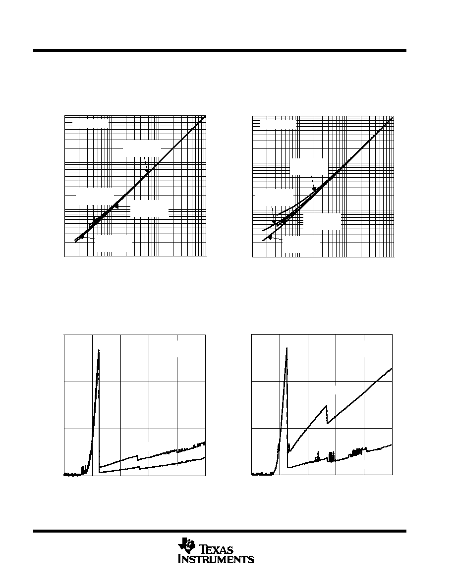
Figure 21
≠
Output V
oltage
≠
mV
TPS60401, TPS60402
OUTPUT VOLTAGE
vs
TIME
V
O
t ≠ Time ≠
µ
s
VI = 5 V
IO = 30 mA
TPS60402
TPS60401
50 mV/DIV
50 mV/DIV
20
µ
s/DIV
Figure 22
≠
Output V
oltage
≠
mV
TPS60400, TPS60403
OUTPUT VOLTAGE
vs
TIME
V
O
t ≠ Time ≠
µ
s
VI = 5 V
IO = 30 mA
TPS60403
TPS60400
100 mV/DIV
50 mV/DIV
4
µ
s/DIV

TPS60400, TPS60401, TPS60402, TPS60403
UNREGULATED 60-mA CHARGE PUMP VOLTAGE INVERTER
SLVS324 ≠ JULY 2001
13
POST OFFICE BOX 655303
∑
DALLAS, TEXAS 75265
APPLICATION INFORMATION
voltage inverter
The most common application for these devices is a charge-pump voltage inverter (see Figure 23). This
application requires only two external components; capacitors C
(fly)
and C
O
, plus a bypass capacitor, if
necessary. Refer to the capacitor selection section for suggested capacitor types.
TPS60400
C1≠
C1+
3
5
OUT
IN
GND
1
2
4
CI
1
µ
F
CO
1
µ
F
≠5 V,
Max 60 mA
Input 5 V
C(fly)
1
µ
F
Figure 23. Typical Operating Circuit
For the maximum output current and best performance, three ceramic capacitors of 1
µ
F (TPS60400,
TPS60403) are recommended. For lower currents or higher allowed output voltage ripple, other capacitors can
also be used. It is recommended that the output capacitors has a minimum value of 1
µ
F. With flying capacitors
lower than 1
µ
F, the maximum output power will decrease.

TPS60400, TPS60401, TPS60402, TPS60403
UNREGULATED 60-mA CHARGE PUMP VOLTAGE INVERTER
SLVS324 ≠ JULY 2001
14
POST OFFICE BOX 655303
∑
DALLAS, TEXAS 75265
APPLICATION INFORMATION
RC-post filter
TPS60400
OUT
C1+
IN
C1≠
GND
1
2
3
5
4
C(fly)
1
µ
F
CO
1
µ
F
CP
CI
1
µ
F
VO (≠VI)
GND
VI
GND
RP
Figure 24. TPS60400 and TPS60401 With RC-Post Filter
An output filter can easily be formed with a resistor (R
P
) and a capacitor (C
P
). Cutoff frequency is given by:
c
+
1
2
p
R
P
C
P
(1)
and ratio V
O
/V
OUT
is:
V
O
V
OUT
+
1
1
)
2
p
R
P
C
P
2
(2)
with R
P
= 50
, C
P
= 0.1
µ
F and f = 250 kHz:
V
O
V
OUT
+
0.125
The formula refers only to the relation between output and input of the ac ripple voltages of the filter.
LC-post filter
TPS60400
OUT
C1+
IN
C1≠
GND
1
2
3
5
4
C(fly)
1
µ
F
CO
1
µ
F
CP
CI
1
µ
F
VO (≠VI)
GND
VI
GND
LP
VOUT
Figure 25. LC-Post Filter
Figure 25 shows a configuration with a LC-post filter to further reduce output ripple and noise.

TPS60400, TPS60401, TPS60402, TPS60403
UNREGULATED 60-mA CHARGE PUMP VOLTAGE INVERTER
SLVS324 ≠ JULY 2001
15
POST OFFICE BOX 655303
∑
DALLAS, TEXAS 75265
APPLICATION INFORMATION
Table 4. Measurement Results on the TPS60400 (Typical)
VI
[V]
IO(2)
[mA]
CI
[
µ
F]
C(fly)
[
µ
F]
CO
[
µ
F]
LP
[
µ
H]
CP
[
µ
F]
BW = 500 MHz
VPOUT
BW = 20 MHz
VPOUT
VPOUT
VACeff [mV]
[V]
( )
[mA]
CERAMIC
CERAMIC
CERAMIC
[
µ
H]
CERAMIC
VPOUT
VP≠P[mV]
VPOUT
VP≠P[mV]
VACeff [mV]
5
60
1
1
1
320
240
65
5
60
1
1
2.2
120
240
32
5
60
1
1
1
0.1 (X7R)
260
200
58
5
60
1
1
1
0.1
0.1 (X7R)
220
200
60
5
60
1
1
2.2
0.1
0.1 (X7R)
120
100
30
5
60
1
1
10
0.1
0.1 (X7R)
50
28
8
rail splitter
TPS60400
OUT
C1+
IN
C1≠
GND
1
2
3
5
4
C(fly)
1
µ
F
CO
1
µ
F
CI
1
µ
F
VO (≠VI)
GND
VI
GND
C3
1
µ
F
Figure 26. TPS60400 as a High-Efficiency Rail Splitter
A switched-capacitor voltage inverter can be configured as a high efficiency rail-splitter. This circuit provides a
bipolar power supply that is useful in battery powered systems to supply dual-rail ICs, like operational amplifiers.
Moreover, the SOT23-5 package and associated components require very little board space.
After power is applied, the flying capacitor (C
(fly)
) connects alternately across the output capacitors C
3
and C
O
.
This equalizes the voltage on those capacitors and draws current from V
I
to V
O
as required to maintain the
output at 1/2 V
I
.
The maximum input voltage between V
I
and GND in the schematic (or between IN and OUT at the device itself)
must not exceed 6.5 V.

TPS60400, TPS60401, TPS60402, TPS60403
UNREGULATED 60-mA CHARGE PUMP VOLTAGE INVERTER
SLVS324 ≠ JULY 2001
16
POST OFFICE BOX 655303
∑
DALLAS, TEXAS 75265
APPLICATION INFORMATION
combined doubler/inverter
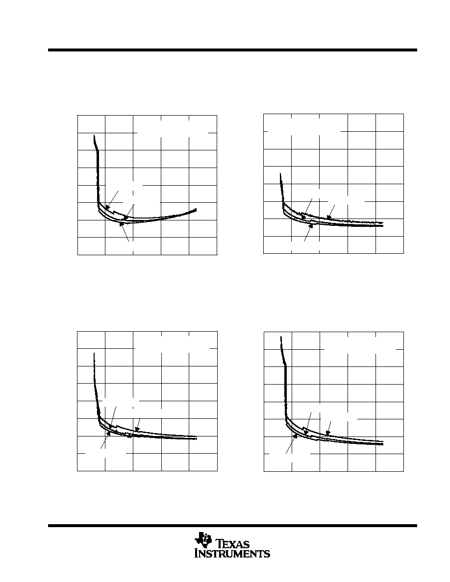
In the circuit of Figure 27, capacitors C
I
, C
(fly)
, and C
O
form the inverter, while C1 and C2 form the doubler. C1
and C
(fly)
are the flying capacitors; C
O
and C2 are the output capacitors. Because both the inverter and doubler
use part of the charge-pump circuit, loading either output causes both outputs to decline toward GND. Make
sure the sum of the currents drawn from the two outputs does not exceed 60 mA. The maximum output current at
V
(pos)
must not exceed 30 mA. If the negative output is loaded, this current must be further reduced.
TPS60400
OUT
C1+
IN
C1≠
GND
1
2
3
5
4
C(fly)
1
µ
F
CO
1
µ
F
CI
1
µ
F
≠VI
GND
GND
VI
C1
+
+
+
D2
C2
+
V(pos)
+
I
I
≠I
O
+ 2
◊
I
O(POS)
Figure 27. TPS60400 as Doubler/Inverter
cascading devices
Two devices can be cascaded to produce an even larger negative voltage (see Figure 28). The unloaded output
voltage is normally ≠2
◊
V
I
, but this is reduced slightly by the output resistance of the first device multiplied by the
quiescent current of the second. When cascading more than two devices, the output resistance rises
dramatically.
TPS60400
OUT
C1+
IN
C1≠
GND
1
2
3
5
4
C(fly)
1
µ
F
CO
1
µ
F
CI
1
µ
F
VO (≠2 VI)
GND
VI
GND
TPS60400
OUT
C1+
IN
C1≠
GND
1
2
3
5
4
CO
1
µ
F
GND
+
+
+
C(fly)
1
µ
F
Figure 28. Doubling Inverter
TPS60400, TPS60401, TPS60402, TPS60403
UNREGULATED 60-mA CHARGE PUMP VOLTAGE INVERTER
SLVS324 ≠ JULY 2001
17
POST OFFICE BOX 655303
∑
DALLAS, TEXAS 75265
APPLICATION INFORMATION
paralleling devices
Paralleling multiple TPS6040xs reduces the output resistance. Each device requires its own flying capacitor
(C
(fly)
), but the output capacitor (C
O
) serves all devices (see Figure 29). Increase C
O
's value by a factor of n,
where n is the number of parallel devices. Equation 1 shows the equation for calculating output resistance.
TPS60400
OUT
C1+
IN
C1≠
GND
1
2
3
5
4
C(fly)
1
µ
F
CI
1
µ
F
VO (≠VI)
GND
VI
GND
TPS60400
OUT
C1+
IN
C1≠
GND
1
2
3
5
4
C(fly)
1
µ
F
CO
2.2
µ
F
+
Figure 29. Paralleling Devices
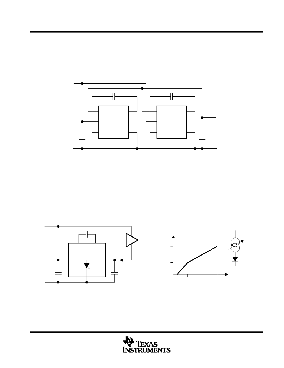
active-Schottky diode
For a short period of time, when the input voltage is applied, but the inverter is not yet working, the output
capacitor is charged positive by the load. To prevent the output being pulled above GND, a Schottky diode must
be added in parallel to the output. The function of this diode is integrated into the TPS6040x devices, which gives
a defined startup performance and saves board space.
A current sink and a diode in series can approximate the behavior of a typical, modern operational amplifier.
Figure 30 shows the current into this typical load at a given voltage. The TPS6040x devices are optimized to
start into these loads.
TPS60400
C1≠
C1+
5
3
OUT
IN
GND
1
2
4
CI
1
µ
F
CO
1
µ
F
C(fly)
1
µ
F
Typical
Load
IO
VO (≠VI)
+V
≠V
VI
GND
60 mA
25 mA
0.4 V 1.25 V
5 V
Load Current
Voltage at the Load
0.4 V
Figure 30. Typical Load
Figure 31. Maximum Start-Up Current

TPS60400, TPS60401, TPS60402, TPS60403
UNREGULATED 60-mA CHARGE PUMP VOLTAGE INVERTER
SLVS324 ≠ JULY 2001
18
POST OFFICE BOX 655303
∑
DALLAS, TEXAS 75265
APPLICATION INFORMATION
shutting down the TPS6040x
If shutdown is necessary, use the circuit in Figure 32. The output resistance of the TPS6040x will typically be
15
plus two times the output resistance of the buffer.
Connecting multiple buffers in parallel can reduce the output resistance of the buffer driving the IN pin.
TPS60400
OUT
C1+
IN
C1≠
GND
1
2
3
5
4
C(fly)
1
µ
F
CO
1
µ
F
CI
1
µ
F
VO (≠VI)
GND
VI
GND
SDN
Figure 32. Shutdown Control
GaAs supply
A solution for a ≠2.7-V/3-mA GaAs bias supply is proposed in Figure 33. The input voltage of 3.3 V is first inverted
with a TPS60403 and stabilized using a TLV431 low-voltage shunt regulator. Resistor R
P
with capacitor C
P
is
used for filtering the output voltage.
TPS60400
OUT
C1+
IN
C1≠
GND
1
2
3
5
4
C(fly)
0.1
µ
F
CO
1
µ
F
CI
0.1
µ
F
VO (≠2.7 V/3 mA)
GND
VI (3.3 V)
GND
RP
TLV431
R2
R1
CP
Figure 33. GaAs Supply
V
O
+ *
1
)
R1
R2
V
ref
*
R1
I
I(ref)
A 0.1-
µ
F capacitor was selected for C
(fly)
. By this, the output resistance of the inverter is about 52
.
TPS60400, TPS60401, TPS60402, TPS60403
UNREGULATED 60-mA CHARGE PUMP VOLTAGE INVERTER
SLVS324 ≠ JULY 2001
19
POST OFFICE BOX 655303
∑
DALLAS, TEXAS 75265
APPLICATION INFORMATION
GaAs supply (continued)
R
PMAX
can be calculated using the following equation:
R
PMAX
+
V
CO
*
V
O
I
O
*
R
O
With: V
CO
= ≠3.3 V; V
O
= ≠2.7 V; I
O
= ≠3 mA
R
PMAX
= 200
≠ 52
= 148
A 100-
resistor was selected for R
P
.
The reference voltage across R2 is 1.24 V typical. With 5-
µ
A current for the voltage divider, R2 gets:
R2
+
1.24 V
5
m
A
[
250 k
W
R1
+
2.7
*
1.24 V
5
m
A
[
300 k
W
With C
P
= 1
µ
F the ratio V
O
/V
I
of the RC post filter is:
V
O
V
I
+
1
1
)
(2
p
125000Hz
100
W
1
m
F)
2
[
0.01
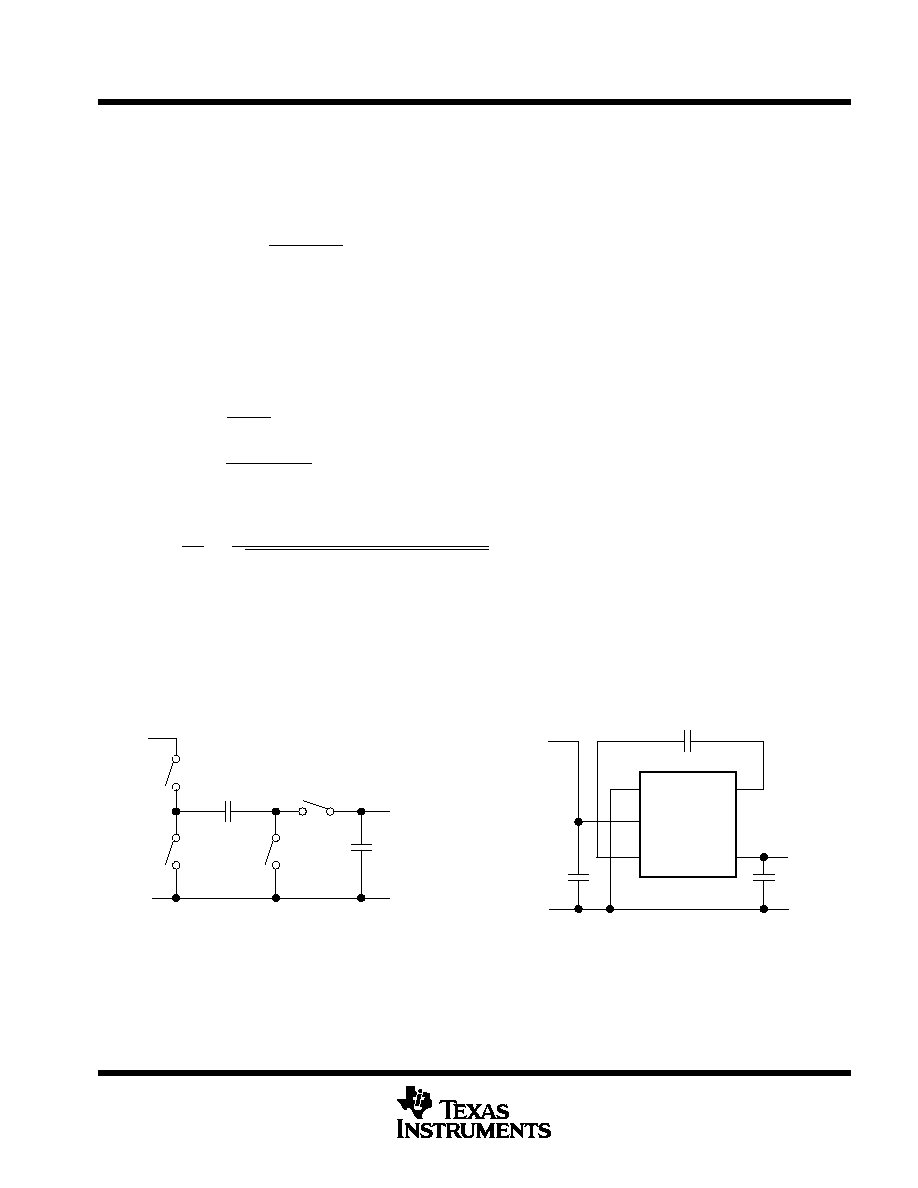
step-down charge pump
By exchanging GND with OUT (connecting the GND pin with OUT and the OUT pin with GND), a step-down
charge pump can easily be formed. In the first cycle S1 and S3 are closed, and C
(fly)
with C
O
in series are
charged. Assuming the same capacitance, the voltage across C
(fly)
and C
O
is split equally between the
capacitors. In the second cycle, S2 and S4 close and both capacitors with V
I
/2 across are connected in parallel.
C(fly)
1
µ
F
S2
S1
S3
S4
CO
1
µ
F
VO (VI/2)
GND
VI
VO (VI/2)
+
Figure 34. Step-Down Principle
TPS60400
OUT
C1+
IN
C1≠
GND
1
2
3
5
4
C(fly)
1
µ
F
CO
1
µ
F
CI
1
µ
F
VO (VI/2)
GND
VI
GND
Figure 35. Step-Down Charge Pump Connection
The maximum input voltage between V
I
and GND in the schematic (or between IN and OUT at the device itself)
must not exceed 6.5 V. For input voltages in the range of 6.5 V to 11 V, an additional Zener-diode is
recommended (see Figure 36).

TPS60400, TPS60401, TPS60402, TPS60403
UNREGULATED 60-mA CHARGE PUMP VOLTAGE INVERTER
SLVS324 ≠ JULY 2001
20
POST OFFICE BOX 655303
∑
DALLAS, TEXAS 75265
APPLICATION INFORMATION
OUT
IN
C1≠
TPS60400
C1+
GND
5
4
1
2
3
C(fly)
1
µ
F
5V6
CO
1
µ
F
CI
1
µ
F
VI
GND
VO ≠ VI
GND
Figure 36.
power dissipation
As given in the data sheet, the thermal resistance of the unsoldered package is R
JA
= 347
∞
C/W. Soldered on
the EVM, a typical thermal resistance of R
JA(EVM)
= 180
∞
C/W was measured.
The terminal resistance can be calculated using the following equation:
R
q
JA
+
T
J
*
T
A
P
D
Where:
T
J
is the junction temperature.
T
A
is the ambient temperature.
P
D
is the power that needs to be dissipated by the device.
R
q
JA
+
T
J
*
T
A
P
D
The maximum power dissipation can be calculated using the following equation:
P
D
= V
I
◊
I
I
≠ V
O
◊
I
O
= V
I(max)
◊
(I
O
+ I
(SUPPLY)
) ≠ V
O
◊
I
O
The maximum power dissipation happens with maximum input voltage and maximum output current.
At maximum load the supply current is 0.7 mA maximum.
P
D
= 5 V
◊
(60 mA + 0.7 mA) ≠ 4.4 V
◊
60 mA = 40 mW
With this maximum rating and the thermal resistance of the device on the EVM, the maximum temperature rise
above ambient temperature can be calculated using the following equation:
T
J
= R
JA
◊
P
D
= 180
∞
C/W
◊
40 mW = 7.2
∞
C
This means that the internal dissipation increases T
J
by
<
10
∞
C.
The junction temperature of the device shall not exceed 125
∞
C.
This means the IC can easily be used at ambient temperatures up to:
T
A
= T
J(max)
≠
T
J
= 125
∞
C/W ≠ 10
∞
C = 115
∞
C
TPS60400, TPS60401, TPS60402, TPS60403
UNREGULATED 60-mA CHARGE PUMP VOLTAGE INVERTER
SLVS324 ≠ JULY 2001
21
POST OFFICE BOX 655303
∑
DALLAS, TEXAS 75265
APPLICATION INFORMATION
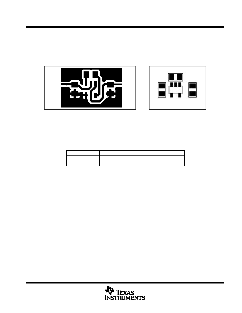
layout and board space
All capacitors should be soldered as close as possible to the IC. A PCB layout proposal for a single-layer board
is shown in Figure 37. Care has been taken to connect all capacitors as close as possible to the circuit to achieve
optimized output voltage ripple performance.
CFLY
CIN
COUT
U1
TPS60400
IN
GND
OUT
Figure 37. Recommended PCB Layout for TPS6040x (top layer)
device family products
Other inverting dc-dc converters from Texas Instruments are listed in Table 5.
Table 5. Product Identification
PART NUMBER
DESCRIPTION
TPS6735
Fixed negative 5
-
V, 200
-
mA inverting dc-dc converter
TPS6755
Adjustable 1
-
W inverting dc-dc converter

TPS60400, TPS60401, TPS60402, TPS60403
UNREGULATED 60-mA CHARGE PUMP VOLTAGE INVERTER
SLVS324 ≠ JULY 2001
22
POST OFFICE BOX 655303
∑
DALLAS, TEXAS 75265
MECHANICAL DATA
DBV (R-PDSO-G5)
PLASTIC SMALL-OUTLINE
0,10
M
0,20
0,95
0
∞
≠8
∞
0,25
0,35
0,55
Gage Plane
0,15 NOM
4073253-4/F 10/00
2,60
3,00
0,50
0,30
1,50
1,70
4
5
3
1
2,80
3,00
0,95
1,45
0,05 MIN
Seating Plane
NOTES: A. All linear dimensions are in millimeters.
B. This drawing is subject to change without notice.
C. Body dimensions do not include mold flash or protrusion.
D. Falls within JEDEC MO-178

IMPORTANT NOTICE
Texas Instruments and its subsidiaries (TI) reserve the right to make changes to their products or to discontinue
any product or service without notice, and advise customers to obtain the latest version of relevant information
to verify, before placing orders, that information being relied on is current and complete. All products are sold
subject to the terms and conditions of sale supplied at the time of order acknowledgment, including those
pertaining to warranty, patent infringement, and limitation of liability.
TI warrants performance of its products to the specifications applicable at the time of sale in accordance with
TI's standard warranty. Testing and other quality control techniques are utilized to the extent TI deems necessary
to support this warranty. Specific testing of all parameters of each device is not necessarily performed, except
those mandated by government requirements.
Customers are responsible for their applications using TI components.
In order to minimize risks associated with the customer's applications, adequate design and operating
safeguards must be provided by the customer to minimize inherent or procedural hazards.
TI assumes no liability for applications assistance or customer product design. TI does not warrant or represent
that any license, either express or implied, is granted under any patent right, copyright, mask work right, or other
intellectual property right of TI covering or relating to any combination, machine, or process in which such
products or services might be or are used. TI's publication of information regarding any third party's products
or services does not constitute TI's approval, license, warranty or endorsement thereof.
Reproduction of information in TI data books or data sheets is permissible only if reproduction is without
alteration and is accompanied by all associated warranties, conditions, limitations and notices. Representation
or reproduction of this information with alteration voids all warranties provided for an associated TI product or
service, is an unfair and deceptive business practice, and TI is not responsible nor liable for any such use.
Resale of TI's products or services with
statements different from or beyond the parameters stated by TI for
that product or service voids all express and any implied warranties for the associated TI product or service,
is an unfair and deceptive business practice, and TI is not responsible nor liable for any such use.
Also see: Standard Terms and Conditions of Sale for Semiconductor Products. www.ti.com/sc/docs/stdterms.htm
Mailing Address:
Texas Instruments
Post Office Box 655303
Dallas, Texas 75265
Copyright
2001, Texas Instruments Incorporated