 | ÐлекÑÑоннÑй компоненÑ: CC1050T | СкаÑаÑÑ:  PDF PDF  ZIP ZIP |
Äîêóìåíòàöèÿ è îïèñàíèÿ www.docs.chipfind.ru
CC1050
SWRS044
Page 1 of 40
CC1050
Single Chip Very Low Power RF Transmitter
Applications
· Very low power UHF wireless data
transmitters
· 315 / 433 / 868 and 915 MHz ISM/SRD
band systems
· RKE Remote Keyless Entry
· Home automation
· Wireless alarm and security systems
· AMR Automatic Meter Reading
· Low power telemetry
· Game Controllers and advanced toys
Product Description
CC1050 is a true single-chip UHF trans-
mitter designed for very low power and
very low voltage wireless applications. The
circuit is mainly intended for the ISM
(Industrial, Scientific and Medical) and
SRD (Short Range Device) frequency
bands at 315, 433, 868 and 915 MHz, but
can easily be programmed for operation at
other frequencies in the 300-1000 MHz
range.
The main operating parameters of
CC1050
can be programmed via an easy-to-
interface serial bus, thus making
CC1050 a
very flexible and easy to use transmitter.
In a typical system
CC1050 will be used
together with a microcontroller and a few
external passive components.
CC1050 is based on Chipcon's SmartRF
®
technology in 0.35
µm CMOS.
Features
· True single chip UHF RF transmitter
· Very low current consumption
· Frequency range 300 1000 MHz
· Programmable output power 20 to
12 dBm
· Small size (TSSOP-24 package)
· Low supply voltage (2.1 V to 3.6 V)
· Very few external components required
· Single-ended antenna connection
· FSK data rate up to 76.8 kBaud
· Complies with EN 300 220 and FCC
CFR47 part 15
· Programmable frequency in 250 Hz
steps makes crystal temperature drift
compensation possible without TCXO
·
Suitable for frequency hopping
protocols
· Development Kit available
· Easy-to-use software for generating the
CC1050 configuration data

CC1050
SWRS044
Page 2 of 40
Table of Contents
Absolute Maximum Ratings ....................................................................................................... 4
Operating Conditions ................................................................................................................. 4
Electrical Specifications ............................................................................................................. 4
Pin Assignment .......................................................................................................................... 7
Application Circuit ...................................................................................................................... 9
Configuration Overview............................................................................................................ 10
Configuration Software............................................................................................................. 11
3-wire Serial Configuration Interface........................................................................................ 12
Microcontroller Interface........................................................................................................... 14
Signal interface ........................................................................................................................ 15
Frequency programming .......................................................................................................... 17
VCO ......................................................................................................................................... 17
VCO and PLL self-calibration................................................................................................... 17
VCO current control ................................................................................................................. 21
Power management ................................................................................................................. 21
Output Matching....................................................................................................................... 24
Output power programming ..................................................................................................... 25
Crystal oscillator....................................................................................................................... 26
Optional LC Filter ..................................................................................................................... 27
System Considerations and Guidelines ................................................................................... 28
PCB Layout Recommendations ............................................................................................... 29
Antenna Considerations........................................................................................................... 29
Configuration registers ............................................................................................................. 30
Package Description (TSSOP-24) ........................................................................................... 38
Soldering Information ............................................................................................................... 38
Plastic Tube Specification........................................................................................................ 38
CC1050
SWRS044
Page 3 of 40
Carrier Tape and Reel Specification ........................................................................................ 38
Ordering Information ................................................................................................................ 39
General Information ................................................................................................................. 39
Address Information ................................................................................................................. 40
CC1050
SWRS044
Page 4 of 40
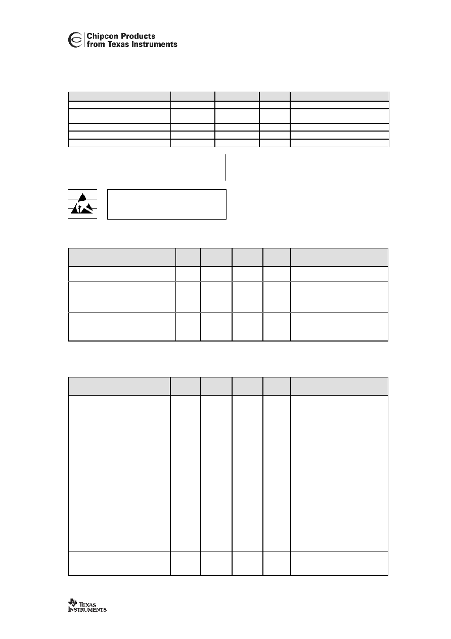
Absolute Maximum Ratings
Parameter
Min.
Max.
Units
Condition
Supply voltage, VDD
-0.3
5.0
V
Voltage on any pin
-0.3
VDD+0.3,
max 5.0
V
Input RF level
10
dBm
Storage temperature range
-50
150
°C
Reflow soldering temperature
260
°C
T = 10 s
Under no circumstances the absolute
maximum ratings given above should be
violated. Stress exceeding one or more of
the limiting values may cause permanent
damage to the device.
Caution! ESD sensitive device.
Precaution should be used when handling
the device in order to prevent permanent
damage.
Operating Conditions
Parameter
Min.
Typ.
Max.
Unit
Condition / Note
RF Frequency Range
300
1000
MHz
Programmable in steps of 250 Hz
Operating ambient temperature range
-40
85
°C
Supply voltage
2.1 3.0 3.6 V
Note: The same supply voltage
should be used for digital (DVDD)
and analogue (AVDD) power.
Electrical Specifications
Tc = 25
°C, VDD = 3.0 V if nothing else stated
Parameter
Min.
Typ.
Max.
Unit Condition / Note
Transmit Section
Transmit data rate
0.6
76.8
kBaud
NRZ or Manchester encoding.
76.8 kBaud equals 76.8 kbit/s
using NRZ coding. See page 15.
Binary FSK frequency separation
0
65
kHz
The frequency separation is
programmable in 250 Hz steps.
65 kHz is the maximum
guaranteed separation at 1 MHz
reference frequency. Larger
separations can be achieved at
higher reference frequencies.
Output power
433 MHz
868 MHz
-20
-20
12
8
dBm
dBm
Delivered to 50
load.
The output power is
programmable.
RF output impedance
433/868 MHz
110 / 70
Transmit mode. For matching
details see p.24.
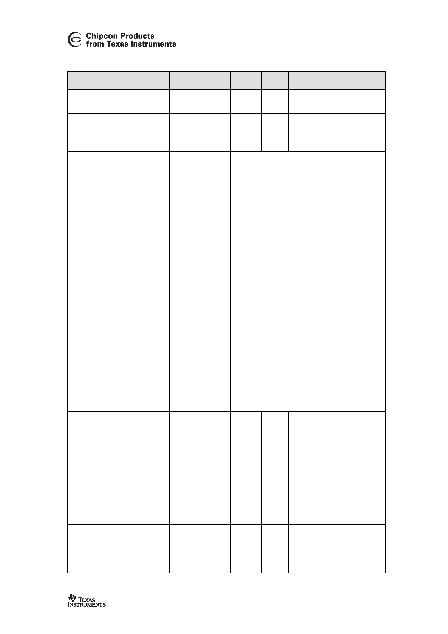
CC1050
SWRS044
Page 5 of 40
Parameter
Min.
Typ.
Max.
Unit Condition / Note
Spurious emission
-36
dBm
Complies with EN 300 220
Harmonics
-20
dBc
An external LC should be used to
reduce harmonics emission to
comply with SRD requirements.
See p.27.
Frequency Synthesiser
Section
Crystal Oscillator Frequency
3
16
MHz
Crystal frequency can be 3-4, 6-8
or 9-16 MHz. Recommended
frequencies are 3.6864, 7.3728,
11.0592 and 14.7456. See page
26 for details.
Crystal frequency accuracy
requirement
± 50
± 25
ppm
433
MHz
868 MHz
The crystal frequency accuracy
and drift (ageing and
temperature dependency) will
determine the frequency accuracy
of the transmitted signal.
Crystal operation
Parallel
C3 and C4 are loading
capacitors, see page 26
Crystal load capacitance
12
12
12
22
16
16
30
30
16
pF
pF
pF
3-8 MHz, 22 pF recommended
6-8 MHz, 16 pF recommended
9-16 MHz, 16 pF recommended
Crystal oscillator start-up time
4
1.5
2
ms
ms
ms
3.6864 MHz, 16 pF load
7.3728 MHz, 16 pF load
16 MHz, 16 pF load
Output signal phase noise
-80
dBc/Hz At 100 kHz offset from carrier
PLL lock time
200
µs
Up to 1 MHz frequency step
PLL turn-on time, crystal oscillator
on in power down mode
250
µs
Crystal oscillator running
Digital Inputs/Outputs
Logic "0" input voltage
0
0.3*VDD
V
Logic "1" input voltage
0.7*VDD
VDD
V
Logic "0" output voltage
0
0.4
V
Output current -2.5 mA,
3.0 V supply voltage
Logic "1" output voltage
2.5
VDD
V
Output current 2.5 mA,
3.0 V supply voltage
Logic "0" input current
NA -1
µA
Input signal equals GND
Logic "1" input current
NA 1
µA
Input signal equals VDD
DI setup time
20
ns
TX mode, minimum time DI must
be ready before the positive edge
of DCLK
DI hold time
10
ns
TX mode, minimum time DI must
be held after the positive edge of
DCLK
Document Outline