 | –≠–ª–µ–∫—Ç—Ä–æ–Ω–Ω—ã–π –∫–æ–º–ø–æ–Ω–µ–Ω—Ç: CC1150RST | –°–∫–∞—á–∞—Ç—å:  PDF PDF  ZIP ZIP |

CC1150
Preliminary Data Sheet (rev. 1.0.)
SWRS037 Page 1 of 49
CC1150 Single Chip Low Cost Low Power RF-Transmitter
Applications
∑ Ultra low power UHF wireless transmitters
∑ 315/433/868 and 915MHz ISM/SRD band
systems
∑ AMR Ò Automatic Meter Reading
∑ Consumer Electronics
∑ RKE Ò Remote Keyless Entry
∑ Low power telemetry
∑ Home and building automation
∑ Wireless alarm and security systems
∑ Industrial monitoring and control
Product Description
The CC1150 is a low cost true single chip UHF
transmitter designed for very low power
wireless applications. The circuit is mainly
intended for the ISM (Industrial, Scientific and
Medical) and SRD (Short Range Device)
frequency bands at 315, 433, 868 and
915MHz, but can easily be programmed for
operation at other frequencies in the 300-
348MHz, 400-464MHz and 800-928MHz
bands.
The RF transmitter is integrated with a highly
configurable baseband modulator. The
modulator supports various modulation
formats and has a configurable data rate up to
500kbps. Performance can be increased by
enabling a Forward Error Correction option,
which is integrated in the modulator.
The CC1150 provides extensive hardware
support for packet handling, data buffering and
burst transmissions.
The main operating parameters and the 64-
byte transmit FIFO of CC1150 can be controlled
via an SPI interface. In a typical system, the
CC1150 will be used together with a micro-
controller and a few additional passive
components.
CC1150 is based on ChipconÌs SmartRF
04
technology in 0.18µm CMOS.
Key Features
∑ Small size (QLP 4x4mm package, 16 pins)
∑ True single chip UHF RF transmitter
∑ Frequency bands: 300-348MHz, 400-
464MHz and 800-928MHz
∑ Programmable data rate up to 500kbps
∑ Low current consumption
∑ Programmable output power up to
+10dBm for all supported frequencies
∑ Very few external components: Totally on-
chip frequency synthesizer, no external
filters needed
∑ Programmable
baseband
modulator
∑ Ideal for multi-channel operation
∑ Configurable packet handling hardware
∑ Suitable for frequency hopping systems
due to a fast settling frequency synthesizer
∑ Optional Forward Error Correction with
interleaving
∑ 64-byte TX data FIFO
∑ Suited for systems compliant with EN 300
220 and FCC CFR Part 15
∑ Many powerful digital features allow a
high-performance RF system to be made
using an inexpensive microcontroller
∑ Efficient SPI interface: All registers can be
programmed with one ÏburstÓ transfer
∑ Integrated
analog
temperature
sensor
∑ Lead-free ÏgreenÓ package

CC1150
Preliminary Data Sheet (rev.1.0.) SWRS037
Page 2 of 49
Features (continued from front page)
∑ Flexible support for packet oriented
systems: On chip support for sync word
insertion, flexible packet length and
automatic CRC handling.
∑ OOK and flexible ASK shaping supported
∑ 2-FSK, GFSK and MSK supported.
∑ Optional automatic whitening of data
∑ Support for asynchronous transparent
transmit mode for backwards compatibility
with existing radio communication
protocols
1 Abbreviations
Abbreviations used in this data sheet are described below.
2-FSK
Binary Frequency Shift Keying
OOK
On-Off-Keying
ADC
Analog to Digital Converter
PA
Power Amplifier
AFC
Automatic Frequency Offset Compensation
PCB
Printed Circuit Board
AGC
Automatic Gain Control
PD
Power Down
AMR
Automatic Meter Reading
PER
Packet Error Rate
ASK
Amplitude Shift Keying
PLL
Phase Locked Loop
BER
Bit Error Rate
PQI
Preamble Quality Indicator
CCA
Clear Channel Assessment
RCOSC
RC Oscillator
CRC
Cyclic Redundancy Check
RF
Radio Frequency
EIRP
Equivalent Isotropic Radiated Power
RSSI
Received Signal Strength Indicator
ESR
Equivalent Series Resistance
RX
Receive, Receive Mode
FEC
Forward Error Correction
SAW
Surface Aqustic Wave
FIFO
First-In-First-Out
SNR
Signal to Noise Ratio
FSK
Frequency Shift Keying
SPI
Serial Peripheral Interface
GFSK
Gaussian shaped Frequency Shift Keying
TBD
To Be Defined
LNA
Low Noise Amplifier
TX
Transmit, Transmit Mode
LO
Local Oscillator
VCO
Voltage Controlled Oscillator
LQI
Link Quality Indicator
XOSC
Crystal Oscillator
MCU Microcontroller
Unit
XTAL Crystal
MSK
Minimum Shift Keying

CC1150
Preliminary Data Sheet (rev. 1.0.) SWRS037
Page 3 of 49
Table Of Contents
1
A
BBREVIATIONS
...................................................................................................................................2
2
A
BSOLUTE
M
AXIMUM
R
ATINGS
...........................................................................................................4
3
O
PERATING
C
ONDITIONS
......................................................................................................................4
4
E
LECTRICAL
S
PECIFICATIONS
...............................................................................................................5
5
G
ENERAL
C
HARACTERISTICS
................................................................................................................5
6
RF
T
RANSMIT
S
ECTION
........................................................................................................................6
7
C
RYSTAL
O
SCILLATOR
.........................................................................................................................6
8
F
REQUENCY
S
YNTHESIZER
C
HARACTERISTICS
.....................................................................................7
9
A
NALOG TEMPERATURE SENSOR
..........................................................................................................7
10
DC
C
HARACTERISTICS
.........................................................................................................................8
11
P
OWER
O
N
R
ESET
.................................................................................................................................8
12
P
IN
C
ONFIGURATION
............................................................................................................................8
13
C
IRCUIT
D
ESCRIPTION
..........................................................................................................................9
14
A
PPLICATION
C
IRCUIT
........................................................................................................................10
15
C
ONFIGURATION
O
VERVIEW
..............................................................................................................11
16
C
ONFIGURATION
S
OFTWARE
..............................................................................................................13
17
4-
WIRE
S
ERIAL
C
ONFIGURATION AND
D
ATA
I
NTERFACE
....................................................................13
17.1
C
HIP
S
TATUS
B
YTE
.............................................................................................................................13
17.2
R
EGISTER
A
CCESS
..............................................................................................................................14
17.3
C
OMMAND
S
TROBES
...........................................................................................................................14
17.4
FIFO
A
CCESS
.....................................................................................................................................14
17.5
PATABLE
A
CCESS
............................................................................................................................14
18
M
ICROCONTROLLER
I
NTERFACE AND
P
IN
C
ONFIGURATION
...............................................................16
18.1
C
ONFIGURATION
I
NTERFACE
..............................................................................................................16
18.2
G
ENERAL
C
ONTROL AND
S
TATUS
P
INS
..............................................................................................16
19
D
ATA
R
ATE
P
ROGRAMMING
...............................................................................................................17
20
P
ACKET
H
ANDLING
H
ARDWARE
S
UPPORT
.........................................................................................17
20.1
D
ATA WHITENING
...............................................................................................................................17
20.2
P
ACKET FORMAT
................................................................................................................................17
20.3
P
ACKET
H
ANDLING IN
T
RANSMIT
M
ODE
............................................................................................19
21
M
ODULATION
F
ORMATS
.....................................................................................................................19
21.1
F
REQUENCY
S
HIFT
K
EYING
................................................................................................................19
21.2
M
INIMUM
S
HIFT
K
EYING
....................................................................................................................19
21.3
A
MPLITUDE
M
ODULATION
.................................................................................................................19
22
F
ORWARD
E
RROR
C
ORRECTION WITH
I
NTERLEAVING
........................................................................20
22.1
F
ORWARD
E
RROR
C
ORRECTION
(FEC)...............................................................................................20
22.2
I
NTERLEAVING
...................................................................................................................................20
23
R
ADIO
C
ONTROL
................................................................................................................................21
23.1
P
OWER ON START
-
UP SEQUENCE
.........................................................................................................22
23.2
C
RYSTAL
C
ONTROL
............................................................................................................................22
23.3
V
OLTAGE
R
EGULATOR
C
ONTROL
.......................................................................................................22
23.4
A
CTIVE
M
ODE
....................................................................................................................................22
23.5
T
IMING
...............................................................................................................................................23
24
D
ATA
FIFO ........................................................................................................................................23
25
F
REQUENCY
P
ROGRAMMING
..............................................................................................................24
26
VCO...................................................................................................................................................25
26.1
VCO
AND
PLL
S
ELF
-C
ALIBRATION
...................................................................................................25
27
V
OLTAGE
R
EGULATORS
.....................................................................................................................25
28
O
UTPUT
P
OWER
P
ROGRAMMING
........................................................................................................25
29
C
RYSTAL
O
SCILLATOR
.......................................................................................................................27
30
A
NTENNA
I
NTERFACE
.........................................................................................................................27
31
G
ENERAL
P
URPOSE
/
T
EST
O
UTPUT
C
ONTROL
P
INS
............................................................................27
32
A
SYNCHRONOUS AND
S
YNCHRONOUS
S
ERIAL
O
PERATION
................................................................30
32.1
A
SYNCHRONOUS OPERATION
..............................................................................................................30
32.2
S
YNCHRONOUS SERIAL OPERATION
....................................................................................................30
CC1150
Preliminary Data Sheet (rev. 1.0.) SWRS037
Page 4 of 49
33
C
ONFIGURATION
R
EGISTERS
..............................................................................................................30
33.1
C
ONFIGURATION
R
EGISTER
D
ETAILS
.................................................................................................34
33.2
S
TATUS REGISTER DETAILS
.................................................................................................................43
34
P
ACKAGE
D
ESCRIPTION
(QLP
16) ......................................................................................................45
34.1
R
ECOMMENDED
PCB
LAYOUT FOR PACKAGE
(QLP
16) .....................................................................46
34.2
P
ACKAGE THERMAL PROPERTIES
........................................................................................................46
34.3
S
OLDERING INFORMATION
..................................................................................................................47
34.4
T
RAY SPECIFICATION
..........................................................................................................................47
34.5
C
ARRIER TAPE AND REEL SPECIFICATION
............................................................................................47
35
O
RDERING
I
NFORMATION
...................................................................................................................47
36
G
ENERAL
I
NFORMATION
.....................................................................................................................47
36.1
D
OCUMENT
H
ISTORY
..........................................................................................................................47
36.2
P
RODUCT
S
TATUS
D
EFINITIONS
..........................................................................................................48
36.3
D
ISCLAIMER
.......................................................................................................................................48
36.4
T
RADEMARKS
.....................................................................................................................................48
36.5
L
IFE
S
UPPORT
P
OLICY
........................................................................................................................48
37
A
DDRESS
I
NFORMATION
.....................................................................................................................49
2 Absolute Maximum Ratings
Under no circumstances must the absolute maximum ratings given in Table 1 be violated. Stress
exceeding one or more of the limiting values may cause permanent damage to the device.
Caution! ESD sensitive device.
Precaution should be used when handling
the device in order to prevent permanent
damage.
Parameter
Min
Max
Units
Condition
Supply voltage
Ò0.3
3.6
V
All supply pins must have the same voltage
Voltage on any digital pin
Ò0.3
VDD+0.3,
max 3.6
V
Voltage on the pins RF_P, RF_N
and DCOUPL
Ò0.3 2.0 V
Input RF level
10
dBm
Storage temperature range
Ò50
150
∞C
Solder reflow temperature
265
∞C
According to IPC/JEDEC J-STD-020C
Table 1: Absolute Maximum Ratings
3 Operating
Conditions
The operating conditions for CC1150 are listed Table 2 in below.
Parameter
Min
Max
Unit
Condition
Operating temperature
-40
85
∞C
Operating supply voltage
1.8
3.6
V
All supply pins must have the same voltage
Table 2: Operating Conditions
CC1150
Preliminary Data Sheet (rev. 1.0.) SWRS037
Page 5 of 49
4 Electrical
Specifications
Tc = 25∞C, VDD = 3.0V if nothing else stated. Measured on ChipconÌs CC1150EM reference design.
Parameter
Min Typ Max Unit Condition
Current consumption
200
nA
Voltage regulator to digital part off, register values retained
(SLEEP state)
180
µA
Voltage regulator to digital part on, all other modules in power
down (XOFF state)
1.4
mA Only voltage regulator to digital part and crystal oscillator running
(IDLE state)
8.0
mA Only the frequency synthesizer running (after going from IDLE
until reaching RX or TX states, and frequency calibration states)
Current consumption,
315MHz
26.3
17.6
14.5
11.2
mA Transmit mode, +10dBm output power
Transmit mode, 5dBm output power
Transmit mode, 0dBm output power
Transmit mode, Ò10dBm output power
Current consumption,
433MHz
26.4
18.0
14.9
13.4
mA Transmit mode, +10dBm output power
Transmit mode, 5dBm output power
Transmit mode, 0dBm output power
Transmit mode, Ò10dBm output power
Current consumption,
868/915MHz
28.7
18.8
15.9
13.7
mA Transmit mode, +10dBm output power
Transmit mode, 5dBm output power
Transmit mode, 0dBm output power
Transmit mode, Ò10dBm output power
Table 3: Electrical Specifications
5 General
Characteristics
Parameter
Min
Typ
Max
Unit
Condition/Note
Frequency range
300
348
MHz
400
464
MHz
800
928
MHz
Data rate
1.2
500
kbps
Modulation formats supported:
(Shaped) MSK (also known as differential offset
QPSK) up to 500kbps
2-FSK up to 500kbps
GFSK and OOK/ASK (up to 250kbps)
Optional Manchester encoding (halves the data rate).
Table 4: General Characteristics

CC1150
Preliminary Data Sheet (rev. 1.0.) SWRS037
Page 6 of 49
6 RF Transmit Section
Tc = 25∞C, VDD = 3.0V, +10dBm if nothing else stated. Measured on ChipconÌs CC1150EM reference design.
Parameter
Min
Typ
Max
Unit
Condition/Note
Differential load
impedance
TBD
Follow CC1150EM reference design
Output power,
highest setting
10
dBm
Output power is programmable, and full range is available
across all frequency bands.
Delivered to a 50 single-ended load via Chipcon reference
RF matching network.
Output power,
lowest setting
Ò30
dBm
Output power is programmable, and full range is available
across all frequency bands.
Delivered to a 50 single-ended load via Chipcon reference
RF matching network.
Spurious emissions
and harmonics,
433/868MHz
Ò36
Ò54
Ò47
Ò30
dBm
dBm
dBm
dBm
25MHz Ò 1GHz
47-74, 87.5-118, 174-230, 470-862MHz
1800MHz-1900MHz (restricted band in Europe), when the
operating frequency is below 900MHz (2
nd
harmonic can not
fall within this band when used in Europe)
Otherwise above 1GHz
Spurious
emissions,
315/915MHz
-49.2
-41.2
dBm
EIRP
dBm
EIRP
<200µV/m at 3m below 960MHz.
<500µV/m at 3m above 960MHz.
Harmonics
315MHz
-20
-41.2
dBc
dBm
2
nd
, 3
rd
and 4
th
harmonic when the output power is maximum
6mV/m at 3m. (-19.6dBm EIRP)
5
th
harmonic
Harmonics
915MHz
-20
-41.2
dBc
dBm
2
nd
harmonic
3
rd
, 4
th
and 5
th
harmonic
Table 5: RF Transmit Parameters
7 Crystal
Oscillator
Tc = 25∞C @ VDD = 3.0 V if nothing else is stated.
Parameter
Min
Typ
Max
Unit
Condition/Note
Crystal frequency
26
26
27
MHz
Tolerance
±40
ppm
This is the total tolerance including a) initial tolerance, b) aging
and c) temperature dependence.
The acceptable crystal tolerance depends on RF frequency and
channel spacing / bandwidth.
ESR
100
Start-up time
300
µs
Measured on ChipconÌs CC1150EM reference design. This
parameter is to a large degree crystal dependent.
Table 6: Crystal Oscillator Parameters
CC1150
Preliminary Data Sheet (rev. 1.0.) SWRS037
Page 7 of 49
8 Frequency
Synthesizer
Characteristics
Tc = 25∞C @ VDD = 3.0 V if nothing else is stated. Measured on ChipconÌs CC1100EM reference design.
Parameter
Min
Typ
Max
Unit
Condition/Note
Programmed
frequency resolution
397 F
XOSC
/
2
16
412
Hz
26MHz-27MHz crystal. The resolution (in Hz) is equal for
all frequency bands.
Synthesizer frequency
tolerance
±40
ppm
Given by crystal used. Required accuracy (including
temperature and aging) depends on frequency band and
channel bandwidth / spacing.
PLL turn-on / hop time
80
µs
Time from leaving the IDLE state until arriving in the
FSTXON or TX state, when not performing calibration.
Crystal oscillator running.
PLL calibration time
0.69
18739
0.72
0.72
XOSC
cycles
ms
Calibration can be initiated manually, or automatically
before entering or after leaving RX/TX.
Min/typ/max time is for 27/26/26MHz crystal frequency.
Table 7: Frequency Synthesizer Parameters
9 Analog
temperature
sensor
The characteristics of the analog temperature sensor are listed in Table 8 below. Note that it is
necessary to write 0xBF to the PTEST register to use the analog temperature sensor in the IDLE
state.
The values in the table are simulated results and will be updated in later versions of the data sheet. Minimum / maximum
values are valid over entire supply voltage range. Typical values are for 3.0V supply voltage.
Parameter
Min
Typ
Max
Unit
Condition/Note
Output voltage at Ò40∞C
0.638 0.648 0.706 V
Output voltage at 0∞C
0.733 0.743 0.793 V
Output voltage at +40∞C
0.828 0.840 0.891 V
Output voltage at +80∞C
0.924 0.939 0.992 V
Temperature coefficient
2.35
2.45
2.46
mV/∞C Fitted from Ò20∞C to +80∞C
Absolute error in calculated
temperature
Ò14 Ò8 +14
∞C From
Ò20∞C to +80∞C when assuming best fit for
absolute accuracy: 0.763V at 0∞C and 2.44mV / ∞C
Error in calculated
temperature, calibrated
Ò2 +2
∞C From
Ò20∞C to +80∞C when using 2.44mV / ∞C,
after 1-point calibration at room temperature
Settling time after enabling
TBD
µs
Current consumption
increase when enabled
0.3
mA
Table 8: Analog Temperature Sensor Parameters
CC1150
Preliminary Data Sheet (rev. 1.0.) SWRS037
Page 8 of 49
10 DC Characteristics
The DC Characteristics of CC1150 are listed in Table 9 below.
Tc = 25∞C if nothing else stated.
Digital Inputs/Outputs
Min
Max
Unit
Condition
Logic "0" input voltage
0
0.7
V
Logic "1" input voltage
VDD-0.7
VDD
V
Logic "0" output voltage
0
0.5
V
For up to 4mA output current
Logic "1" output voltage
VDD-0.3
VDD
V
For up to 4mA output current
Logic "0" input current
N/A
Ò1
µA
Input equals 0V
Logic "1" input current
N/A
1
µA
Input equals VDD
Table 9: DC Characteristics
11 Power On Reset
When the power supply complies with the requirements in Table 10 below, proper Power-On-
Reset functionality is guaranteed. Otherwise, the chip should be assumed to have unknown state
until transmitting an SRES strobe over the SPI interface. It is recommended to transmit an SRES
strobe after turning power on in any case. See section 23.1 on page 22 for a description of the
recommended start up sequence after turning power on.
Parameter
Min Typ Max Unit Condition/Note
Power-up ramp-up time.
5
ms
From 0V until reaching 1.8V
Power off time
1
ms
Minimum time between power-on and power-off.
Table 10: Power-on Reset Requirements
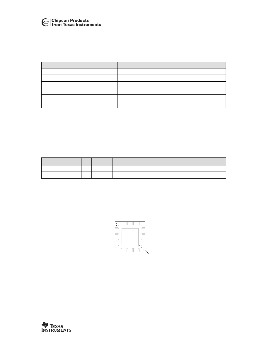
12 Pin Configuration
GND
Exposed die
attach pad
5
XOS
C
_
Q
1
6
AVDD
7
XOS
C
_
Q
2
8
GD
O0
(
A
T
E
S
T
)
9 CSn
10 RF_P
11 RF_N
12 AVDD
13
AVDD
14
RB
IAS
15
D
G
UA
RD
16
SI
1
SCLK
2
SO (GDO1)
3
DVDD
4
DCOUPL
Figure 1: Pinout top view
Note: The exposed die attach pad must be connected to a solid ground plane as this is the main
ground connection for the chip.
CC1150
Preliminary Data Sheet (rev. 1.0.) SWRS037
Page 9 of 49
Pin # Pin name
Pin type
Description
1
SCLK
Digital Input
Serial configuration interface, clock input
2
SO
(
GDO1
)
Digital Output
Serial configuration interface, data output.
Optional general output pin when
CSn
is high
3
DVDD
Power (Digital)
1.8V-3.6V digital power supply for digital I/OÌs and for the digital core
voltage regulator
4
DCOUPL
Power (Digital)
1.6V-2.0V digital power supply output for decoupling.
NOTE: This pin is intended for use with the CC1150 only. It can not be
used to provide supply voltage to other devices.
5
XOSC_Q1
Analog I/O
Crystal oscillator pin 1, or external clock input
6
AVDD
Power (Analog)
1.8V-3.6V analog power supply connection
7
XOSC_Q2
Analog I/O
Crystal oscillator pin 2
8
GDO0
(ATEST)
Digital I/O
Digital output pin for general use:
∑ Test
signals
∑ FIFO
status
signals
∑ Clock output, down-divided from XOSC
∑ Serial input TX data
Also used as analog test I/O for prototype/production testing
9
CSn
Digital Input
Serial configuration interface, chip select
10
RF_P
RF I/O
Positive RF output signal from PA
11
RF_N
RF I/O
Negative RF output signal from PA
12
AVDD
Power (Analog)
1.8V-3.6V analog power supply connection
13
AVDD
Power (Analog)
1.8V-3.6V analog power supply connection
14
RBIAS
Analog I/O
External bias resistor for reference current
15
DGUARD
Power (Digital)
Power supply connection for digital noise isolation
16
SI
Digital Input
Serial configuration interface, data input
Table 11: Pinout overview
13 Circuit Description
BIAS
XOSC_Q1 XOSC_Q2
XOSC
FREQ
SYNTH
RADIO CONTROL
RF_P
RF_N
CSn
SI
SO (GDO1)
SCLK
GDO0 (ATEST)
RBIAS
PA
FE
C
/
IN
T
E
RL
EA
V
E
R
P
A
CKE
T
HANDLE
R
MO
DUL
ATO
R
TX
FI
FO
DIG
I
TAL
I
N
TE
R
F
ACE
TO
M
C
U
Figure 2: CC1150 Simplified Block Diagram
A simplified block diagram of CC1150 is shown
in Figure 2.
The CC1150 transmitter is based on direct
synthesis of the RF frequency. The frequency
synthesizer includes a completely on-chip LC
VCO.
A crystal is to be connected to XOSC_Q1 and
XOSC_Q2. The crystal oscillator generates the

CC1150
Preliminary Data Sheet (rev. 1.0.) SWRS037
Page 10 of 49
reference frequency for the synthesizer, as
well as clocks for the digital part.
A 4-wire SPI serial interface is used for
configuration and data buffer access.
The digital baseband includes support for
channel configuration, packet handling and
data buffering.
14 Application Circuit
Only a few external components are required
for using the CC1150. The recommended
application circuit is shown in Figure 3. The
external components are described in Table
12, and typical values are given in Table 13.
Bias resistor
The bias resistor R141 is used to set an
accurate bias current.
Balun and RF matching
C101, C111, L101 and L111 form a balun that
converts the differential RF port on CC1150 to a
single-ended RF signal (C104 is also needed
for DC blocking). Together with an appropriate
LC network, the balun components also
transform the impedance to match a 50
antenna (or cable). Component values for the
RF balun and LC network are easily found
using the SmartRF
Studio software.
Suggested values for 315MHz, 433MHz and
868/915MHz are listed in Table 13.
Crystal
The crystal oscillator uses an external crystal
with two loading capacitors (C51 and C71).
See section 29 on page 27 for details.
Additional filtering
Additional external components (e.g. an RF
SAW filter) may be used in order to improve
the performance in specific applications.
Power supply decoupling
The power supply must be properly decoupled
close to the supply pins. Note that decoupling
capacitors are not shown in the application
circuit. The placement and the size of the
decoupling capacitors are very important to
achieve the optimum performance. Chipcon
provides a reference design that should be
followed closely.
Component
Description
C41
100nF decoupling capacitor for on-chip voltage regulator to digital part
C51/C71
Crystal loading capacitors, see section 29 on page 27 for details
C101/C111 RF
balun/matching
capacitors
C102/C103
RF LC filter/matching capacitors
C104
RF balun DC blocking capacitor
C105
RF LC filter DC blocking capacitor (only needed if there is a DC path in the antenna)
L101/L111
RF balun/matching inductors (inexpensive multi-layer type)
L102/L103
RF LC filter/matching inductor (inexpensive multi-layer type)
R141 56k resistor for internal bias current reference
XTAL
26MHz-27MHz crystal, see section 29 on page 27 for details
Table 12: Overview of external components (excluding supply decoupling capacitors)

CC1150
Preliminary Data Sheet (rev. 1.0.) SWRS037
Page 11 of 49
D
i
g
i
ta
l
In
te
fa
ce
1.8V-3.6V power supply
8
GD
O0
5
XO
SC_
Q
1
6
AVDD
7
XO
SC_
Q
2
SI
1
6
DG
UA
RD 1
5
RBI
A
S 1
4
AV
DD 1
3
1 SCLK
2 SO
(GDO1)
3 DVDD
4 DCOUPL
AVDD 12
RF_N 11
RF_P 10
CSn 9
XTAL
R141
C51
C71
C41
CSn
GDO0
(optional)
SO
(GDO1)
SCLK
SI
CC1150
DIE ATTACH PAD:
DCOUPL
XO
S
C
_
Q
1
Antenna
(50 Ohm)
L102
L103
C102
C103
C105
C111
C101
L101
L111
C104
Figure 3: Typical application and evaluation circuit (power supply decoupling not shown)
Component
Value at 315MHz
Value at 433MHz
Value at 868/915MHz
C41
100nF±10%, 0402 X5R
C51
27pF±5%, 0402 NP0
C71
27pF±5%, 0402 NP0
C101
6.8pF±0.5pF, 0402 NP0
3.9pF±0.25pF, 0402 NP0
2.2pF±0.25pF, 0402 NP0
C102
12pF±5%, 0402 NP0
8.2pF±0.5pF, 0402 NP0
3.9pF±0.25pF, 0402 NP0
C103
6.8pF±0.5pF, 0402 NP0
5.6pF±0.5pF, 0402 NP0
3.3pF±0.25pF, 0402 NP0
C104
220pF±5%, 0402 NP0
220pF±5%, 0402 NP0
100pF±5%, 0402 NP0
C105
220pF±5%, 0402 NP0
220pF±5%, 0402 NP0
100pF±5%, 0402 NP0
C111
6.8pF±0.5pF, 0402 NP0
3.9pF±0.25pF, 0402 NP0
2.2pF±0.25pF, 0402 NP0
L101
33nH±5%, 0402 monolithic
27nH±5%, 0402 monolithic
12nH±5%, 0402 monolithic
L102
18nH±5%, 0402 monolithic
22nH±5%, 0402 monolithic
5.6nH±0.3nH, 0402 monolithic
L103
33nH±5%, 0402 monolithic
27nH±5%, 0402 monolithic
12nH±5%, 0402 monolithic
L111
33nH±5%, 0402 monolithic
27nH±5%, 0402 monolithic
12nH±5%, 0402 monolithic
R141 56k±1%, 0402
XTAL
26.0MHz surface mount crystal
Table 13: Bill Of Materials for the application circuit (subject to changes)
15 Configuration Overview
CC1150 can be configured to achieve optimum
performance for many different applications.
Configuration is done using the SPI interface.
The following key parameters can be
programmed:
∑ Power-down / power-up mode

CC1150
Preliminary Data Sheet (rev. 1.0.) SWRS037
Page 12 of 49
∑ Crystal oscillator power-up / power Ò down
∑ Transmit
mode
∑ RF
channel
selection
∑ Data
rate
∑ Modulation
format
∑ RF output power
∑ Data buffering with 64-byte transmit FIFO
∑ Packet radio hardware support
∑ Forward Error Correction with interleaving
∑ Data
Whitening
Details of each configuration register can be
found in section 33, starting on page 30.
Figure 4 shows a simplified state diagram that
explains the main CC1150 states, together with
typical usage and current consumption. For
detailed information on controlling the CC1150
state machine, and a complete state diagram,
see section 23, starting on page 21.
Transmit mode
IDLE
Manual freq.
synth. calibration
TX FIFO
underflow
Frequency
synthesizer on
SFSTXON
STX
STX
SFTX
SIDLE
SCAL
IDLE
TXOFF_MODE=00
SRX or STX or SFSTXON or wake-on-radio (WOR)
Sleep
SPWD or wake-on-radio (WOR)
Crystal
oscillator off
SXOFF
CSn=0
CSn=0
TXOFF_MODE=01
Frequency
synthesizer startup,
optional calibration,
settling
Optional freq.
synth. calibration
Default state when the radio is not
receiving or transmitting. Typ.
current consumption: 1.4mA.
Lowest power mode.
Register values are lost.
Current consumption typ
200nA.
All register values are
retained. Typ. current
consumption; 0.18mA.
Used for calibrating frequency
synthesizer upfront (entering
transmit mode can then be
done quicker). Transitional
state. Typ. current
consumption: 8.0mA.
Frequency synthesizer is turned on, can optionally be
calibrated, and then settles to the correct frequency.
Transitional state. Typ. current consumption: 8.0mA.
Frequency synthesizer is on,
ready to start transmitting.
Transmission starts very
quickly after receiving the
STX command strobe.Typ.
current consumption: 8.0mA.
Typ. current consumption:
13mA at -10dBm output,
15mA at 0dBm output,
18mA at +5dBm output,
27mA at +10dBm output.
Optional transitional state. Typ.
current consumption: 8.0mA.
In FIFO-based modes,
transmission is turned off and
this state entered if the TX
FIFO becomes empty in the
middle of a packet. Typ.
current consumption: 1.4mA.
Figure 4: Simplified state diagram, with typical usage and current consumption
CC1150
Preliminary Data Sheet (rev. 1.0.) SWRS037
Page 13 of 49
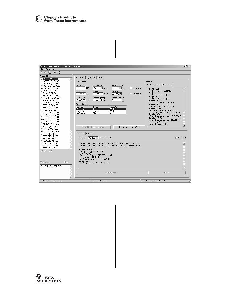
16 Configuration Software
CC1150 can be configured using the SmartRF
Studio software, available for download from
http://www.chipcon.com. The SmartRF
Studio
software is highly recommended for obtaining
optimum register settings, and for evaluating
performance and functionality. A screenshot of
the SmartRF
Studio user interface for CC1150
is shown in Figure 5.
Figure 5: SmartRF
Studio user interface
17 4-wire Serial Configuration and Data Interface
CC1150 is configured via a simple 4-wire SPI-
compatible interface (SI, SO, SCLK and CSn)
where CC1150 is the slave. This interface is
also used to read and write buffered data. All
address and data transfer on the SPI interface
is done most significant bit first.
All transactions on the SPI interface start with
a header byte containing a read/write bit, a
burst access bit and a 6-bit address.
During address and data transfer, the CSn pin
(Chip Select, active low) must be kept low. If
CSn
goes high during the access, the transfer
will be cancelled.
When CSn goes low, the MCU must wait until
the CC1150 SO pin goes low before starting to
transfer the header byte. This indicates that
the voltage regulator has stabilized and the
crystal is running. Unless the chip was in the
SLEEP or XOFF states, the SO pin will always
go low immediately after taking CSn low.
17.1 Chip
Status
Byte
When the header byte is sent on the SPI
interface, the chip status byte is sent by the
CC1150 on the SO pin. The status byte contains
key status signals, useful for the MCU. The
first bit, s7, is the CHIP_RDYn signal; this

CC1150
Preliminary Data Sheet (rev. 1.0.) SWRS037
Page 14 of 49
signal must go low before the first positive
edge of SCLK. The CHIP_RDYn signal
indicates that the crystal is running and the
regulated digital supply voltage is stable.
Bit 6, 5 and 4 comprises the STATE value. This
value reflects the state of the chip. When idle
the XOSC and power to the digital core is on,
but all other modules are in power down. The
frequency and channel configuration should
only be updated when the chip is in this state.
The TX state will be active when the chip is in
transmit mode.
The last four bits (3:0) in the status byte con-
tains FIFO_BYTES_AVAILABLE. This field
contains the number of bytes free for writing
into the TX FIFO. When
FIFO_BYTES_AVAILABLE=15
, 15 or more
bytes are free.
17.2 Register
Access
The configuration registers on the CC1150 are
located on SPI addresses from 0x00 to 0x2F.
Table 24 on page 32 lists all configuration
registers. The detailed description of each
register is found in Section 33.1, starting on
page 34. All configuration registers can be
both written and read. The read/write bit
controls if the register should be written or
read. When writing to registers, the status byte
is sent on the SO pin each time a data byte to
be written is transmitted on the SI pin.
Registers with consecutive addresses can be
accessed in an efficient way by setting the
burst bit in the address header. The address
sets the start address in an internal address
counter. This counter is incremented by one
each new byte (every 8 clock pulses). The
burst access is either a read or a write access
and must be terminated by setting CSn high.
For register addresses in the range 0x30-
0x3D, the ÏburstÓ bit is used to select between
status registers and command strobes (see
below). The status registers can only be read.
Burst read is not available for status registers,
so they must be read one at a time.
17.3 Command
Strobes
Command Strobes may be viewed as single
byte instructions to CC1150. By addressing a
Command Strobe register, internal sequences
will be started. These commands are used to
disable the crystal oscillator, enable transmit
mode, flush the TX FIFO etc. The nine
command strobes are listed in Table 23 on
page 31.
The command strobe registers are accessed
in the same way as for a register write
operation, but no data is transferred. That is,
only the R/W bit (set to 0), burst access (set to
0) and the six address bits (in the range 0x30
through 0x3D) are written. A command strobe
may be followed by any other SPI access
without pulling CSn high. The command
strobes are executed immediately, with the
exception of the SPWD and the SXOFF strobes
that are executed when CSn goes high.
17.4 FIFO
Access
The 64-byte TX FIFO is accessed through the
0x3F addresses. When the read/write bit is
zero, the TX FIFO is accessed. The TX FIFO
is write-only.
The burst bit is used to determine if FIFO
access is single byte or a burst access. The
single byte access method expects address
with burst bit set to zero and one data byte.
After the data byte a new address is expected;
hence, CSn can remain low. The burst access
method expects one address byte and then
consecutive data bytes until terminating the
access by setting CSn high.
The following header bytes access the FIFO:
∑ 0x3F: Single byte access to TX FIFO
∑ 0x7F: Burst access to TX FIFO
When writing to the TX FIFO, the status byte
(see Section 17.1) is output for each new data
byte on SO, as shown in Figure 6. This status
byte can be used to detect TX FIFO underflow
while writing data to the TX FIFO. Note that
the status byte contains the number of bytes
free before writing the byte in progress to the
TX FIFO. When the last byte that fits in the TX
FIFO is transmitted to the SI pin, the status
byte received concurrently on the SO pin will
indicate that one byte is free in the TX FIFO.
The transmit FIFO may be flushed by issuing a
SFTX
command strobe. The FIFO is cleared
when going to the SLEEP state.
17.5 PATABLE
Access
The 0x3E address is used to access the
PATABLE
, which is used for selecting PA
power control settings. The SPI expects up to

CC1150
Preliminary Data Sheet (rev. 1.0.) SWRS037
Page 15 of 49
eight data bytes after receiving the address.
By programming the PATABLE, controlled PA
power ramp-up and ramp-down can be
achieved, as well as ASK modulation shaping
for reduced bandwidth. See section 28 on
page 25 for output power programming details.
The PATABLE is an 8-byte table that defines
the PA control settings to use for each of the
eight PA power values (selected by the 3-bit
value FREND0.PA_POWER). The table is
written to and read from the lowest setting (0)
to the highest (7), one byte at a time. An index
counter is used to control the access to the
table. This counter is incremented each time a
byte is read or written to the table, and set to
the lowest index when CSn is high. When the
highest value is reached the counter restarts at
zero.
The access to the PATABLE is either single
byte or burst access depending on the burst
bit. When using burst access the index counter
will count up; when reaching 7 the counter will
restart at 0. The read/write bit controls whether
the access is a write access (R/W=0) or a read
access (R/W=1).
If one byte is written to the PATABLE and this
value is to be read out then CSn must be set
high before the read access in order to set the
index counter back to zero.
Note that the content of the PATABLE is lost
when entering the SLEEP state.
0
A6
A5
A4
A3
A2
A0
A1
D
W
7
D
W
6
D
W
5
D
W
4
D
W
3
D
W
2
D
W
1
D
W
0
1
A6
A5
A4
A3
A2
A0
A1
D
R
7
D
R
6
D
R
5
D
R
4
D
R
3
D
R
2
D
R
1
D
R
0
Read from register:
Write to register:
Hi-Z
X
SCLK:
CSn:
SI
SO
SI
SO
Hi-Z
t
sp
t
ch
t
cl
t
sd
t
hd
t
ns
X
X
Hi-Z
X
S7
S
6
S
5
S
4
S
3
S
2
S
1
S
0
Hi-Z
S7
S
6
S
5
S
4
S
3
S
2
S
1
S
0
S7
S
6
S
5
S
4
S
3
S
2
S
1
S
0
S7
X
Figure 6: Configuration registers write and read operations
Parameter
Description
Min
Max
F
SCLK
SCLK
frequency
0
10MHz
t
sp,pd
CSn
low to positive edge on SCLK, in power-down mode
TBDµs
-
t
sp
CSn
low to positive edge on SCLK, in active mode
TBDns -
t
ch
Clock
high
50ns
-
t
cl
Clock
low
50ns
-
t
rise
Clock rise time
-
TBDns
t
fall
Clock rise time
-
TBDns
t
sd
Setup data to positive edge on SCLK
TBDns
-
t
hd
Hold data after positive edge on SCLK
TBDns
-
t
ns
Negative edge on SCLK to
CSn
high.
TBDns -
Table 14: SPI interface timing requirements

CC1150
Preliminary Data Sheet (rev. 1.0.) SWRS037
Page 16 of 49
Bits Name
Description
7
CHIP_RDYn
Stays high until power and crystal have stabilized. Should always be low when using
the SPI interface.
6:4
STATE[2:0]
Indicates the current main state machine mode
Value State
Description
000 Idle
IDLE
state
(Also reported for some transitional states instead
of SETTLING or CALIBRATE, due to a small error)
001 Not
used
(RX)
Not used, included for software compatibility
with CC1100 transceiver
010 TX
Transmit
mode
011 FSTXON
Fast
TX
ready
100
CALIBRATE
Frequency synthesizer calibration is running
101 SETTLING
PLL
is
settling
110 Not
used
(RXFIFO_OVERFLOW)
Not used, included for software compatibility
with CC1100 transceiver
111
TXFIFO_UNDERFLOW TX FIFO has underflowed. Acknowledge with
SFTX
3:0
FIFO_BYTES_AVAILABLE[3:0] The number of free bytes in the TX FIFO. If FIFO_BYTES_AVAILABLE=15, it
indicates that 15 or more bytes are available/free.
Table 15: Status byte summary
DATA
byte 0
ADDR
FIFO
DATA
byte 1
DATA
byte 2
DATA
byte n-1
DATA
byte n
...
ADDR
strobe
DATA
ADDR
strobe
ADDR
reg
ADDR
reg n
DATA
n
DATA
n+1
DATA
n+2
...
ADDR
strobe
...
CSn:
Command strobe(s):
Read or write register(s):
Read or write consecutive registers (burst):
DATA
ADDR
reg
DATA
ADDR
reg
...
DATA
byte 0
ADDR
FIFO
DATA
byte 1
Combinations:
DATA
ADDR
reg
DATA
ADDR
reg
ADDR
strobe
ADDR
strobe
...
Read or write n+1 bytes from/to RF FIFO:
Figure 7: Register access types
18 Microcontroller Interface and Pin Configuration
In a typical system, CC1150 will interface to a
microcontroller. This microcontroller must be
able to:
∑ Program
CC1150 into different modes,
∑ Write
buffered
data
∑ Read back status information via the 4-wire
SPI-bus configuration interface (SI, SO,
SCLK
and CSn).
18.1 Configuration
Interface
The microcontroller uses four I/O pins for the
SPI configuration interface (SI, SO, SCLK and
CSn
). The SPI is described in Section 0 on
page 12.
18.2 General Control and Status Pins
The CC1150 has one dedicated configurable
pin and one shared pin that can output internal
status information useful for control software.
These pins can be used to generate interrupts
on the MCU. See Section 31 page 27 for more
details of the signals that can be programmed.
The dedicated pin is called GDO0. The shared
pin is the SO pin in the SPI interface. The
default setting for GDO1/SO is 3-state output.
By selecting any other of the programming

CC1150
Preliminary Data Sheet (rev. 1.0.) SWRS037
Page 17 of 49
options the GDO1/SO pin will become a
generic pin. When CSn is low, the pin will
always function as a normal SO pin.
In the synchronous and asynchronous serial
modes, the GDO0 pin is used as a serial TX
data input pin while in transmit mode.
The GDO0 pin can also be used for an on-chip
analog temperature sensor. By measuring the
voltage on the GDO0 pin with an external ADC,
the temperature can be calculated.
Specifications for the temperature sensor are
found in section 9 on page 7.
The temperature sensor output is usually only
available when the frequency synthesizer is
enabled (e.g. the MANCAL, FSTXON and TX
states). It is necessary to write 0xBF to the
PTEST
register to use the analog temperature
sensor in the IDLE state. Before leaving the
IDLE state, the PTEST register should be
restored to its default value (0x7F).
19 Data Rate Programming
The data rate used when transmitting is
programmed by the MDMCFG3.DRATE_M and
the
MDMCFG4.DRATE_E
configuration
registers. The data rate is given by the formula
below. As the formula shows, the programmed
data rate depends on the crystal frequency.
(
)
XOSC
E
DRATE
DATA
f
M
DRATE
R
+
=
28
_
2
2
_
256
The following approach can be used to find
suitable values for a given data rate:
256
2
2
_
2
log
_
_
28
20
2
-
=
=
E
DRATE
XOSC
DATA
XOSC
DATA
f
R
M
DRATE
f
R
E
DRATE
If DRATE_M is rounded to the nearest integer
and becomes 256, increment DRATE_E and
use DRATE_M=0.
20 Packet Handling Hardware Support
The CC1150 has built-in hardware support for
packet oriented radio protocols.
In transmit mode, the packet handler will add
the following elements to the packet stored in
the TX FIFO:
∑ A programmable number of preamble
bytes.
∑ A two byte Synchronization Word. Can be
duplicated to give a 4-byte sync word.
∑ Optionally whiten the data with a PN9
sequence.
∑ Optionally Interleave and Forward Error
Code the data.
∑ Optionally compute and add a CRC
checksum over the data field.
The recommended setting is 4-byte preamble
and 2-byte sync word.
20.1 Data
whitening
From a radio perspective, the ideal over the air
data are random and DC free. This results in
the smoothest power distribution over the
occupied bandwidth. This also gives the
regulation loops in the receiver uniform
operation conditions (no data dependencies).
Real world data often contain long sequences
of zeros and ones. Performance can then be
improved by whitening the data before
transmitting, and de-whitening in the receiver.
With CC1150, in combination with a CC1100 at
the receiver end, this can be done
automatically by setting WHITE_DATA=1 in the
PKTCTRL0
register. All data, except the
preamble and the sync word, are then XOR-ed
with a 9-bit pseudo-random (PN9) sequence
before being transmitted. At the receiver end,
the data are XOR-ed with the same pseudo-
random sequence. This way, the whitening is
reversed, and the original data appear in the
receiver.
Setting PKTCTRL0.WHITE_DATA=1 is recom-
mended for all uses, except when over-the-air
compatibility with other systems is needed.
20.2 Packet
format
The format of the data packet can be
configured and consists of the following items:
∑ Preamble
∑ Synchronization
word
∑ Length byte or constant programmable
packet length

CC1150
Preliminary Data Sheet (rev. 1.0.) SWRS037
Page 18 of 49
∑ Optional
Address
byte
∑ Payload
∑ Optional 2 byte CRC
The preamble pattern is an alternating
sequence of ones and zeros (01010101÷ ).
The minimum length of the preamble is
programmable. When enabling TX, the
modulator will start transmitting the preamble.
When the programmed number of preamble
bytes has been transmitted, the modulator will
send the sync word and then data from the TX
FIFO if data is available. If the TX FIFO is
empty, the modulator will continue to send
preamble bytes until the first byte is written to
the TX FIFO. The modulator will then send the
sync word and then the data bytes.
The number of preamble bytes is programmed
with the MDMCFG1.NUM_PREAMBLE value.
The synchronization word is a two-byte value
set in the SYNC1 and SYNC0 registers. The
sync word provides byte synchronization of the
incoming packet. A one-byte synch word can
be emulated by setting the SYNC1 value to the
preamble pattern. It is also possible to emulate
a 32 bit sync word by using
MDMCFG2.SYNC_MODE=
3 or 7. The sync word
will then be repeated twice.
CC1150 supports both constant packet length
protocols and variable length protocols.
Variable or fixed packet length mode can be
used for packet up to 255 bytes. For longer
packets, infinite packet length mode must be
used.
Fixed packet length mode is selected by
setting PKTCTRL0.LENGTH_CONFIG=0. The
desired packet length is set by the PKTLEN
register. The packet length is defined as the
payload data, excluding the length byte and
the optional automatic CRC. In variable length
mode, PKTCTRL0.LENGTH_CONFIG=1, the
packet length is configured by the first byte
after the sync word.
With PKTCTRL0.LENGTH_CONFIG=2, the
packet length is set to infinite and transmission
and reception will continue until turned off
manually. The infinite mode can be turned off
while a packet is being transmitted or received.
As described in the next section, this can be
used to support packet formats with different
length configuration than natively supported by
CC1150.
Note that the minimum packet length
supported (excluding the optional length byte
and CRC) is one byte of payload data.
20.2.1 Arbitrary length field configuration
By utilizing the infinite packet length option,
arbitrary packet length is available. At the start
of the packet, the infinite mode must be active.
When less than 256 bytes remains of the
packet, the MCU sets the PKTLEN register to
mod(length, 256)
, disables infinite packet
length and activates fixed length packets.
When the internal byte counter reaches the
PKTLEN
value, the packet transmission ends.
Automatic CRC appending can be used (by
setting PKTCTRL0.CRC_EN to 1).
When for example a 454-byte packet is to be
transmitted, the MCU does the following:
∑ Set
PKTCTRL0.LENGTH_CONFIG
=2 (10).
∑ Pre-program the PKTLEN register to
mod(454,256)=198.
∑ Transmit at least 198 bytes, for example
by filling the 64-byte TX FIFO four times
(256 bytes transmitted).
∑ Set
PKTCTRL0.LENGTH_CONFIG
=0 (00).
∑ The transmission ends when the packet
counter reaches 198. A total of
256+198=454 bytes are transmitted.
Preamble bits
(1010...1010)
Sy
n
c
w
o
rd
Lengt
h f
i
eld
A
ddr
es
s
f
i
eld
Data field
CRC
-
1
6
Optional CRC-16 calculation
Optionally FEC encoded/decoded
8 x n bits
16/32 bits
8
bits
8
bits
8 x n bits
16 bits
Optional data whitening
Legend:
Inserted automatically in TX,
processed and removed in RX.
Optional user-provided fields processed in TX,
processed but not removed in RX.
Unprocessed user data (apart from FEC
and/or whitening)
Figure 8: Packet Format

CC1150
Preliminary Data Sheet (rev. 1.0.) SWRS037
Page 19 of 49
20.3 Packet Handling in Transmit Mode
The payload that is to be transmitted must be
written into the TX FIFO. The first byte written
must be the length byte when variable packet
length is enabled. The length byte has a value
equal to the payload of the packet (including
the optional address byte). If fixed packet
length is enabled, then the first byte written to
the TX FIFO is interpreted as the destination
address, if this feature is enabled in the device
that receives the packet.
The modulator will first send the programmed
number of preamble bytes. If data is available
in the TX FIFO, the modulator will send the
two-byte (optionally 4-byte) sync word and
then the payload in the TX FIFO. If CRC is
enabled, the checksum is calculated over all
the data pulled from the TX FIFO and the
result is sent as two extra bytes at the end of
the payload data.
If whitening is enabled, the length byte,
payload data and the two CRC bytes will be
whitened. This is done before the optional
FEC/Interleaver stage. Whitening is enabled
by setting PKTCTRL0.WHITE_DATA=1.
If FEC/Interleaving is enabled, the length byte,
payload data and the two CRC bytes will be
scrambled by the interleaver, and FEC
encoded before being modulated.
21 Modulation Formats
CC1150 supports amplitude, frequency and
phase shift modulation formats. The desired
modulation format is set in the
MDMCFG2.MOD_FORMAT
register.
Optionally, the data stream can be Manchester
coded by the modulator. This option is enabled
by setting MDMCFG2.MANCHESTER_EN=1.
Manchester encoding is not supported at the
same time as using the FEC/Interleaver
option. Manchester coding can be used with
the 2-ary modulation formats (2-FSK, GFSK,
ASK/OOK and MSK).
21.1 Frequency
Shift
Keying
2-FSK can optionally be shaped by a
Gaussian filter with BT=1, producing a GFSK
modulated signal.
The frequency deviation is programmed with
the DEVIATION_M and DEVIATION_E values
in the DEVIATN register. The value has an
exponent/mantissa form, and the resultant
deviation is given by:
E
DEVIATION
xosc
dev
M
DEVIATION
f
f
_
17
2
)
_
8
(
2
+
=
The symbol encoding is shown in Table 16.
Format
Symbol
Coding
2-FSK/GFSK Î0Ì Ò
Deviation
Î1Ì +
Deviation
Table 16: Symbol encoding for 2-FSK/GFSK
modulation
21.2 Minimum
Shift
Keying
When using MSK
1
, the complete transmission
(preamble, sync word and payload) will be
MSK modulated.
Phase shifts are performed with a constant
transition time. This means that the rate of
change for the 180-degree transition is twice
that of the 90-degree transition.
The fraction of a symbol period used to
change the phase can be modified with the
DEVIATN.DEVIATION_M
setting. This is
equivalent to changing the shaping of the
symbol. Setting DEVIATN.DEVIATION_M=7
will generate a standard shaped MSK signal.
21.3 Amplitude
Modulation
CC1150 supports two different forms of
amplitude modulation: On-Off Keying (OOK)
and Amplitude Shift Keying (ASK). OOK
modulation simply turns on or off the PA to
modulate 1 and 0 respectively. When using
ASK the modulation depth (the difference
between 1 and 0) can be programmed, and
the power ramping will be shaped. This will
produce a more bandwidth constrained output
spectrum.
1
Identical to offset QPSK with half-sine
shaping (data coding may differ)

CC1150
Preliminary Data Sheet (rev. 1.0.) SWRS037
Page 20 of 49
22 Forward Error Correction with Interleaving
22.1 Forward Error Correction (FEC)
CC1150 has built in support for Forward Error
Correction (FEC) that can be used with CC1100
at the receiver end. To enable this option, set
MDMCFG1.FEC_EN
to 1. FEC is employed on
the data field and CRC word in order to reduce
the gross bit error rate when operating near
the sensitivity limit. Redundancy is added to
the transmitted data in such a way that the
receiver can restore the original data in the
presence of some bit errors.
The use of FEC allows correct reception at a
lower SNR, thus extending communication
range. Alternatively, for a given SNR, using
FEC decreases the bit error rate (BER). As the
packet error rate (PER) is related to BER by:
length
packet
BER
PER
_
)
1
(
1
-
-
=
,
a lower BER can be used to allow significantly
longer packets, or a higher percentage of
packets of a given length, to be transmitted
successfully. Finally, in realistic ISM radio
environments, transient and time-varying
phenomena will produce occasional errors
even in otherwise good reception conditions.
FEC will mask such errors and, combined with
interleaving of the coded data, even correct
relatively long periods of faulty reception (burst
errors).
The FEC scheme adopted for CC1150 is
convolutional coding, in which n bits are
generated based on k input bits and the m
most recent input bits, forming a code stream
able to withstand a certain number of bit errors
between each coding state (the m-bit window).
The convolutional coder is a rate 1/2 code with
a constraint length of m=4. The coder codes
one input bit and produces two output bits;
hence, the effective data rate is halved.
22.2 Interleaving
Data received through real radio channels will
often experience burst errors due to
interference and time-varying signal strengths.
In order to increase the robustness to errors
spanning multiple bits, interleaving is used
when FEC is enabled. After de-interleaving, a
continuous span of errors in the received
stream will become single errors spread apart.
CC1150 employs matrix interleaving, which is
illustrated in Figure 9. The on-chip interleaving
and de-interleaving buffers are 4 x 4 matrices.
In the transmitter, the data bits are written into
the rows of the matrix, whereas the bit
sequence to be transmitted is read from the
columns of the matrix and fed to the rate
convolutional coder. Conversely, in a CC1100
receiver, the received symbols are written into
the columns of the matrix, whereas the data
passed onto the convolutional decoder is read
from the rows of the matrix.
When FEC and interleaving is used, the
amount of data transmitted over the air must
be a multiple of the size of the interleaver
buffer (two bytes). In addition, at least one
extra byte is required for trellis termination.
The packet control hardware therefore
automatically inserts one or two extra bytes at
the end of the packet, so that the total length
of the data to be interleaved is an even
number. Note that these extra bytes are
invisible to the user, as they are removed
before the received packet enters the RX FIFO
in a CC1100.
Due to the implementation of the FEC and
interleaver, the data to be interleaved must be
at least two bytes. One byte long fixed length
packets without CRC is therefore not
supported when FEC/interleaving is enabled.
Receiver
Transmitter
1) Storing coded
data
2) Transmitting
interleaved data
4) Passing on data
to decoder
3) Receiving
interleaved data
TX
Data
De
m
o
du
la
to
r
Mo
du
la
t
o
r
En
co
d
e
r
RX
Data
De
c
o
de
r
Figure 9: General principle of matrix interleaving

CC1150
Preliminary Data Sheet (rev. 1.0.) SWRS037
Page 21 of 49
23 Radio Control
TX
19,20
IDLE
1
CALIBRATE
8
MANCAL
3,4,5
SETTLING
9,10
TX_UNDERFLOW
22
FSTXON
18
SFSTXON
FS_AUTOCAL = 00 | 10 | 11
&
STX | SFSTXON
STX
STX
TXFIFO_UNDERFLOW
SFTX
SIDLE
SCAL
CAL_COMPLETE
FS_AUTOCAL = 01
&
STX | SFSTXON
CAL_COMPLETE
CALIBRATE
12
IDLE
1
TXOFF_MODE = 00
&
FS_AUTOCAL = 10 | 11
TXOFF_MODE = 00
&
FS_AUTOCAL = 00 | 01
TXOFF_MODE = 10
FS_WAKEUP
6,7
STX | SFSTXON
SLEEP
0
SPWD
XOFF
2
SXOFF
CSn = 0
CSn = 0
TXOFF_MODE = 01
Figure 10: Complete Radio Control State Diagram
CC1150 has a built-in state machine that is
used to switch between different operation
states (modes). The change of state is done
either by using command strobes or by
internal events such as TX FIFO underflow.
A simplified state diagram, together with
typical usage and current consumption, is
shown in Figure 4 on page 12. The complete
radio control state diagram is shown in Figure
10. The numbers refer to the state number
readable in the MARCSTATE status register.
This functionality is primarily for test purposes.

CC1150
Preliminary Data Sheet (rev. 1.0.) SWRS037
Page 22 of 49
23.1 Power on start-up sequence
When the power supply is turned on, the
system must be reset. One of the following two
sequences must be followed: Automatic
power-on reset or manual reset.
A power-on reset circuit is included in the
CC1150. The minimum requirements stated in
Section 11 must be followed for the power-on
reset to function properly. The internal power-
up sequence is completed when CHIP_RDYn
goes low. CHIP_RDYn is observed on the SO
pin after CSn is pulled low. See Section 17.1
for more details on CHIP_RDYn.
The other global reset possibility on CC1150 is
the SRES command strobe. By issuing this
strobe, all internal registers and states are set
to the default, idle state. The power-up
sequence is as follows (see Figure 11):
∑ Set
SCLK=1
and
SI
=0.
∑ Strobe
CSn
low / high.
∑ Hold
CSn
high for at least 40µs.
∑ Pull
CSn
low and wait for SO to go low
(CHIP_RDYn).
∑ Issue
the
SRES
strobe.
∑ When SO goes low again, reset is
complete and the chip is in the IDLE state.
CSn
SO
40µs
SRES
done
Unknown/ don't care
Figure 11: Power-up with SRES
It is recommended to always send a SRES
command strobe on the SPI interface after
power-on even though power-on reset is used.
23.2 Crystal
Control
The crystal oscillator is automatically turned on
when CSn goes low. It will be turned off if the
SXOFF
or SPWD command strobes are issued;
the state machine then goes to XOFF or
SLEEP respectively. This can be done from
any state. The XOSC will be turned off when
CSn
is released (goes high). The XOSC will be
automatically turned on again when CSn goes
low. The state machine will then go to the
IDLE state. The SO pin on the SPI interface
must be zero before the SPI interface is ready
to be used; as described in Section 0 on page
13.
Crystal oscillator start-up time depends on
crystal ESR and load capacitances. The
electrical specification for the crystal oscillator
can be found in section 7 on page 6.
23.3 Voltage
Regulator
Control
The voltage regulator to the digital core is
controlled by the radio controller. When the
chip enters the SLEEP state, which is the state
with the lowest current consumption, this
regulator is disabled. This occurs after CSn is
released when a SPWD command strobe has
been sent on the SPI interface. The chip is
now in the SLEEP state. Setting CSn low again
will turn on the regulator and crystal oscillator
and make the chip enter the IDLE state.
On the CC1150, all register values (with the
exception of the MCSM0.PO_TIMEOUT field)
are lost in the SLEEP state. After the chip gets
back to the IDLE state, the registers will have
default (reset) contents and must be
reprogrammed over the SPI interface.
23.4 Active
Mode
The active transmit mode is activated by the
MCU by using the STX command strobe.
The frequency synthesizer must be calibrated
regularly. CC1150 has one manual calibration
option (using the SCAL strobe), and three
automatic calibration options, controlled by the
MCSM0.FS_AUTOCAL
setting:
∑ Calibrate when going from IDLE to TX
(or FSTXON)
∑ Calibrate when going from TX to IDLE
∑ Calibrate every fourth time when going
from TX to IDLE
The calibration takes a constant number of
XOSC cycles (see Table 17 for timing details).
When TX is active, the chip will remain in the
TX state until the current packet has been
successfully transmitted. Then the state will
change as indicated by the
MCSM1.TXOFF_MODE
setting. The possible
destinations are:
∑ IDLE

CC1150
Preliminary Data Sheet (rev. 1.0.) SWRS037
Page 23 of 49
∑ FSTXON: Frequency synthesizer on
and ready at the TX frequency.
Activate TX with STX.
∑ TX: Start sending preambles
The SIDLE command strobe can always be
used to force the radio controller to go to the
IDLE state.
23.5 Timing
The radio controller controls most timing in
CC1150, such as synthesizer calibration and
PLL lock. Timing from IDLE to TX is constant,
dependent on the auto calibration setting. The
calibration time is constant 18739 clock
periods. Table 17 shows timing in crystal clock
cycles for key state transitions.
Power on time and XOSC start-up times are
variable, but within the limits stated in Table 6.
Description
XOSC
periods
26MHz
crystal
Idle to TX/FSTXON, no calibration
2298
88.4µs
Idle to TX/FSTXON, with calibration
~21037
809µs
TX to IDLE, no calibration
2
0.1µs
TX to IDLE, including calibration
~18739
721µs
Manual calibration
~18739
721µs
Table 17: State transition timing
24 Data FIFO
The CC1150 contains a 64 byte FIFO for data to
be transmitted. The SPI interface is used for
writing to the TX FIFO. Section 17.4 contains
details on the SPI FIFO access. The FIFO
controller will detect underflow in the TX FIFO.
When writing to the TX FIFO it is the
responsibility of the MCU to avoid TX FIFO
overflow. This will not be detected by the
CC1150.
The chip status byte that is available on the SO
pin while transferring the SPI address contains
the fill grade of the TX FIFO. Section 17.1 on
page 13 contains more details on this.
The number of bytes in the TX FIFO can also
be read from the TXBYTES.NUM_TXBYTES
status register.
The 4-bit FIFOTHR.FIFO_THR setting is used
to program the FIFO threshold point. Table 18
lists the 16 FIFO_THR settings and the
corresponding thresholds for the TX FIFO.
A flag will assert when the number of bytes in
the FIFO is equal to or higher than the
programmed threshold. The flag is used to
generate the FIFO status signals that can be
viewed on the GDO pins (see Section 31 on
page 27).
Figure 13 shows the number of bytes in the TX
FIFO when the threshold flag toggles, in the
case of FIFO_THR=13. Figure 12 shows the
flag as the FIFO is filled above the threshold,
and then drained below.
6 7 8 9
6
7
8
9
10
NUM_TXBYTES
GDO
Figure 12: FIFO_THR=13 vs. number of bytes
in FIFO
CC1150
Preliminary Data Sheet (rev. 1.0.) SWRS037
Page 24 of 49
FIFO_THR
Bytes in TX FIFO
0 (0000)
61
1 (0001)
57
2 (0010)
53
3 (0011)
49
4 (0100)
45
5 (0101)
41
6 (0110)
37
7 (0111)
33
8 (1000)
29
9 (1001)
25
10 (1010)
21
11 (1011)
17
12 (1100)
13
13 (1101)
9
14 (1110)
5
15 (1111)
1
Table 18: FIFO_THR settings and the
corresponding FIFO thresholds
8 bytes
Underflow
margin
FIFO_THR=13
TXFIFO
Figure 13: Example of FIFO at threshold
25 Frequency Programming
The frequency programming in CC1150 is
designed to minimize the programming
needed in a channel-oriented system.
To set up a system with channel numbers, the
desired channel spacing is programmed with
the
MDMCFG0.CHANSPC_M
and
MDMCFG1.CHANSPC_E
registers. The channel
spacing registers are mantissa and exponent
respectively.
The base or start frequency is set by the 24 bit
frequency word located in the FREQ2, FREQ1
and FREQ0 registers. This word will typically
be set to the centre of the lowest channel
frequency that is to be used.
The desired channel number is programmed
with the 8-bit channel number register,
CHANNR.CHAN
, which is multiplied by the
channel offset. The resultant carrier frequency
is given by:
(
)
(
)
2
_
16
2
_
256
2
-
+
+
=
E
CHANSPC
XOSC
carrier
M
CHANSPC
CHAN
FREQ
f
f
If any frequency programming register is
altered when the frequency synthesizer is
running, the synthesizer may give an
undesired response. Hence, the frequency
programming should only be updated when
the radio is in the IDLE state.

CC1150
Preliminary Data Sheet (rev. 1.0.) SWRS037
Page 25 of 49
26 VCO
The VCO is completely integrated on-chip.
26.1 VCO and PLL Self-Calibration
The VCO characteristics will vary with
temperature and supply voltage changes, as
well as the desired operating frequency. In
order to ensure reliable operation, CC1150
includes frequency synthesizer self-calibration
circuitry. This calibration should be done
regularly, and must be performed after turning
on power and before using a new frequency
(or channel). The number of XOSC cycles for
completing the PLL calibration is given in
Table 17 on page 27.
The calibration can be initiated automatically
or manually. The synthesizer can be
automatically calibrated each time the
synthesizer is turned on, or each time the
synthesizer is turned off. This is configured
with the MCSM0.FS_AUTOCAL register setting.
In manual mode, the calibration is initiated
when the SCAL command strobe is activated
in the IDLE mode. The default setting is to
calibrate each time the frequency synthesizer
is turned on.
The calibration values are not maintained in
sleep mode. Therefore, the CC1150 must be
recalibrated after reprogramming the
configuration registers when the chip has been
in the SLEEP state.
27 Voltage Regulators
CC1150 contains several on-chip linear voltage
regulators, which generate the supply voltage
needed by low-voltage modules. These
voltage regulators are invisible to the user, and
can be viewed as integral parts of the various
modules. The user must however make sure
that the absolute maximum ratings and
required pin voltages in Table 1 and Table 11
are not exceeded. The voltage regulator for
the digital core requires one external
decoupling capacitor.
Setting the CSn pin low turns on the voltage
regulator to the digital core and starts the
crystal oscillator. The SO pin on the SPI
interface must go low before using the serial
interface (setup time is TBD).
On initial power up, the MCU must set CSn low
and issue the reset command strobe SRES.
If the chip is programmed to enter power-down
mode, (SPWD strobe issued), the power will be
turned off after CSn goes high. The power and
crystal oscillator will be turned on again when
CSn
goes low.
The voltage regulator output should only be
used for driving the CC1150.
28 Output Power Programming
The RF output power level from the device has
two levels of programmability, as illustrated in
Figure 14. Firstly, the special PATABLE
register can hold up to eight user selected
output power settings. Secondly, the 3-bit
FREND0.PA_POWER
value selects the
PATABLE
entry to use. This two-level
functionality provides flexible PA power ramp
up and ramp down at the start and end of
transmission, as well as ASK modulation
shaping. In each case, all the PA power
settings in the PATABLE from index 0 up to the
FREND0.PA_POWER
value are used.
CC1150
Preliminary Data Sheet (rev. 1.0.) SWRS037
Page 26 of 49
e.g 6
PA_POWER[2:0]
in FREND0 register
PATABLE(0)[7:0]
PATABLE(1)[7:0]
PATABLE(2)[7:0]
PATABLE(3)[7:0]
PATABLE(4)[7:0]
PATABLE(5)[7:0]
PATABLE(6)[7:0]
PATABLE(7)[7:0]
Index into PATABLE(7:0)
The PA uses
this setting.
Settings 0 to
PA_POWER are
used during ramp-
up at start of
transmission and
ramp-down at end
of transmission,
and for ASK/OOK
modulation.
The SmartRF
∆
Studio software
should be used to
get optimum
PATABLE settings
for various output
powers.
Figure 14: PA_POWER and PATABLE
The power ramping at the start and at the end
of a packet can be turned off by setting
FREND0.PA_POWER
to zero and then
programming the desired output power to
index zero in the PATABLE.
Table 19 contains recommended PATABLE
settings for various output levels and
frequency bands. See section 17.5 on page 14
for PATABLE programming details.
Table 20 contains output power and current
consumption for default PATABLE setting
(0xC6).
With ASK modulation, the eight power settings
are used for shaping. The modulator contains
a counter that counts up when transmitting a
one and down when transmitting a zero. The
counter counts at a rate equal to 8 times the
symbol rate. The counter saturates at
FREND0.PA_POWER
and 0 respectively. This
counter value is used as an index for a lookup
in the power table. Thus, in order to utilize the
whole table, FREND0.PA_POWER should be 7
when ASK is active. The shaping of the ASK
signal is dependent on the configuration of the
PATABLE
.
315MHz
433MHz
868MHz
915MHz
Output
power
[dBm]
Setting
Current
consumption,
typ. [mA]
Setting
Current
consumption,
typ. [mA]
Setting
Current
consumption,
typ. [mA]
Setting
Current
consumption,
typ. [mA]
-30
0x12 10.3 0x03 10.9 0x01 11.5 0x10 11.4
-20
0x0E 10.7 0x0D 11.4 0x0B 12.1 0x09 11.8
-10
0x6E 11.2 0x34 13.4 0x25 13.8 0x33 13.6
-5
0x68 12.3 0x68 12.9 0x68 13.7 0x68 13.4
0
0x60 14.5 0x60 14.9 0x60 16.2 0x50 15.7
5
0x85 17.6 0x85 18.0 0x86 19.1 0x85 18.5
7
0xCC 21.4 0xCA 22.4 0xCC 24.4 0xC8 24.5
10
0xC3 26.3 0xC2 26.4 0xC3 28.6 0xC0 28.9
Table 19: Optimum PATABLE settings for various output power levels and frequency bands
315MHz
433MHz
868MHz
915MHz
Default
power
setting
Output
power
[dBm]
Current
consumption,
typ. [mA]
Output
power
[dBm]
Current
consumption,
typ. [mA]
Output
power
[dBm]
Current
consumption,
typ. [mA]
Output
power
[dBm]
Current
consumption,
typ. [mA]
0xC6
9.2 24.3 8.4 24.2 8.9 26.9 7.7 25.3
Table 20: Output power and current consumption for default PATABLE setting

CC1150
Preliminary Data Sheet (rev. 1.0.) SWRS037
Page 27 of 49
29 Crystal Oscillator
A crystal in the frequency range 26MHz-
27MHz must be connected between the
XOSC_Q1 and XOSC_Q2 pins. The oscillator
is designed for parallel mode operation of the
crystal. In addition, loading capacitors (C51
and C71) for the crystal are required. The
loading capacitor values depend on the total
load capacitance, C
L
, specified for the crystal.
The total load capacitance seen between the
crystal terminals should equal C
L
for the
crystal to oscillate at the specified frequency.
parasitic
L
C
C
C
C
+
+
=
71
51
1
1
1
The parasitic capacitance is constituted by pin
input capacitance and PCB stray capacitance.
Total parasitic capacitance is typically 2.5pF.
The crystal oscillator circuit is shown in Figure
15. Typical component values for different
values of C
L
are given in Table 21.
The crystal oscillator is amplitude regulated.
This means that a high current is used to start
up the oscillations. When the amplitude builds
up, the current is reduced to what is necessary
to maintain approximately 0.4Vpp signal
swing. This ensures a fast start-up, and keeps
the drive level to a minimum. The ESR of the
crystal should be within the specification in
order to ensure a reliable start-up (see section
7 on page 6).
The initial tolerance, temperature drift, aging
and load pulling should be carefully specified
in order to meet the required frequency
accuracy in a certain application. By specifying
the total expected frequency accuracy in
SmartRF Studio together with data rate and
frequency deviation, the software calculates
the total bandwidth and compares this to the
chosen receiver channel filter bandwidth. The
software reports any contradictions, and a
more accurate crystal is recommended if
required.
XOSC_Q1
XOSC_Q2
XTAL
C51
C71
Figure 15: Crystal oscillator circuit
Component
C
L
= 10pF
C
L
=13pF
C
L
=16pF
C51 15pF 22pF
27pF
C71 15pF 22pF
27pF
Table 21: Crystal oscillator component values
30 Antenna Interface
The balanced RF output of CC1150 is designed
for a simple, low-cost matching and balun
network on the printed circuit board. A few
passive external components ensure proper
matching.
Although CC1150 has a balanced RF output,
the chip can be connected to a single-ended
antenna with few external low cost capacitors
and inductors.
31 General Purpose / Test Output Control Pins
The two digital output pins GDO0 and GDO1 are
general control pins. Their functions are
programmed by IOCFG0.GDO0_CFG and
IOCFG1.GDO1_CFG
respectively. Table 22
shows the different signals that can be
monitored on the GDO pins. These signals can
be used as an interrupt to the MCU. GDO1 is
the same pin as the SO pin on the SPI
interface, thus the output programmed on this
pin will only be valid when CSn is high. The

CC1150
Preliminary Data Sheet (rev. 1.0.) SWRS037
Page 28 of 49
default value for GDO1 is 3-stated, which is
useful when the SPI interface is shared with
other devices.
The default value for GDO0 is a 125kHz-
146kHz clock output (XOSC frequency divided
by 192). Since the XOSC is turned on at
power-on-reset, this can be used to clock the
MCU in systems with only one crystal. When
the MCU is up and running, it can change the
clock frequency by writing to
IOCFG0.GDO0_CFG.
This will not produce
any clock glitches.
An on-chip analog temperature sensor is
enabled by writing the value 128 (0x80h) to the
IOCFG0.GDO0_CFG
register. The voltage on
the GDO0 pin is then proportional to
temperature. See section 9 on page 7 for
temperature sensor specifications.
CC1150
Preliminary Data Sheet (rev. 1.0.) SWRS037
Page 29 of 49
GDO0
_CFG[5:0]
GDO1
_CFG[5:0]
Description
0 (0x00)
Reserved Ò defined on the transceiver version.
1 (0x01)
Reserved Ò defined on the transceiver version.
2 (0x02)
Asserts when the TX FIFO is filled above TXFIFO_THR. De-asserts when the TX FIFO is below TXFIFO_THR.
3 (0x03)
Asserts when TX FIFO is full. De-asserts when the TX FIFO is drained below TXFIFO_THR.
4 (0x04)
Reserved Ò defined on the transceiver version.
5 (0x05)
Asserts when the TX FIFO has underflowed. De-asserts when the FIFO is flushed.
6 (0x06)
Asserts when sync word has been sent, and de-asserts at the end of the packet. The pin will also de-assert if the TX
FIFO underflows.
7 (0x07)
Reserved Ò defined on the transceiver version.
8 (0x08)
Reserved Ò defined on the transceiver version.
9 (0x09)
Reserved Ò defined on the transceiver version.
10 (0x0A) Lock detector output
11 (0x0B) Serial Clock. Synchronous to the data in synchronous serial mode.
Data is set up on the falling edge and is read on the rising edge of SERIAL_CLK.
12 (0x0C) Reserved Ò defined on the transceiver version.
13 (0x0D) Reserved Ò defined on the transceiver version.
14 (0x0E) Reserved Ò defined on the transceiver version.
15 (0x0F) Reserved Ò defined on the transceiver version.
16 (0x10)
Reserved Ò used for test.
17 (0x11)
Reserved Ò used for test.
18 (0x12)
Reserved Ò used for test.
19 (0x13)
Reserved Ò used for test.
20 (0x14)
Reserved Ò used for test.
21 (0x15)
Reserved Ò used for test.
22 (0x16)
Reserved Ò defined on the transceiver version.
23 (0x17)
Reserved Ò defined on the transceiver version.
24 (0x18)
Reserved Ò used for test.
25 (0x19)
Reserved Ò used for test.
26 (0x1A) Reserved Ò used for test.
27 (0x1B) PA_PD. PA is enabled when 1, in power-down when 0. Can be used to control external PA or RX/TX switch.
28 (0x1C) Reserved Ò defined on the transceiver version.
29 (0x1D) Reserved Ò defined on the transceiver version.
30 (0x1E) Reserved Ò used for test.
31 (0x1F) Reserved Ò used for test.
32 (0x20)
Reserved Ò used for test.
33 (0x21)
Reserved Ò used for test.
34 (0x22)
Reserved Ò used for test.
35 (0x23)
Reserved Ò used for test.
36 (0x24) Reserved Ò used for test.
37 (0x25)
Reserved Ò used for test.
38 (0x26)
Reserved Ò used for test.
39 (0x27)
Reserved Ò used for test.
40 (0x28)
Reserved Ò used for test.
41 (0x29)
CHIP_RDY
42 (0x2A) Reserved Ò used for test.
43 (0x2B) XOSC_STABLE
44 (0x2C) Reserved Ò used for test.
45 (0x2D)
GDO0
_Z_EN_N. When this output is 0, GDO0 is configured as input (for serial TX data).
46 (0x2E) High impedance (3-state)
47 (0x2F) HW to 0 (HW1 achieved with _INV signal)
48 (0x30)
CLK_XOSC/1
49 (0x31)
CLK_XOSC/1.5
50 (0x32)
CLK_XOSC/2
51 (0x33)
CLK_XOSC/3
52 (0x34)
CLK_XOSC/4
53 (0x35)
CLK_XOSC/6
54 (0x36)
CLK_XOSC/8
55 (0x37)
CLK_XOSC/12
56 (0x38)
CLK_XOSC/16
57 (0x39)
CLK_XOSC/24
58 (0x3A) CLK_XOSC/32
59 (0x3B) CLK_XOSC/48
60 (0x3C) CLK_XOSC/64
61 (0x3D) CLK_XOSC/96
62 (0x3E) CLK_XOSC/128
63 (0x3F) CLK_XOSC/192
Table 22: GDO signal selection

CC1150
Preliminary Data Sheet (rev. 1.0.) SWRS037
Page 30 of 49
32 Asynchronous and Synchronous Serial Operation
Several features and modes of operation have
been included in the CC1150 to provide
backward compatibility with previous Chipcon
products and other existing RF communication
systems. For new systems, it is recommended
to use the built-in packet handling features, as
they can give more robust communication,
significantly offload the microcontroller and
simplify software development.
32.1 Asynchronous
operation
For backward compatibility with systems
already using the asynchronous data transfer
from other Chipcon products, asynchronous
transfer is also included in CC1150. When
asynchronous transfer is enabled, several of
the support mechanisms for the MCU that are
included in CC1150 will be disabled, such as
packet handling hardware, buffering in the
FIFO and so on. The asynchronous transfer
mode does not allow the use of the data
whitener, interleaver and FEC.
Only 2-FSK, GFSK and ASK/OOK are
supported for asynchronous transfer.
Setting
PKTCTRL0.PKT_FORMAT
to 3
enables asynchronous transparent (serial)
mode.
In TX, the GDO0 pin is used for data input (TX
data).
The MCU must control start and stop of
transmit with the STX and SIDLE strobes.
The CC1150 modulator samples the level of the
asynchronous input 8 times faster than the
programmed data rate. The timing requirement
for the asynchronous stream is that the error in
the bit period must be less than one eighth of
the programmed data rate.
32.2 Synchronous
serial
operation
In the Synchronous serial operation mode,
data is transferred on a two wire serial
interface. The CC1150 provides a clock that is
used to set up new data on the data input line.
Data input (TX data) is the GDO0 pin. This pin
will automatically be configured as an input
when TX is active.
Preamble and sync word insertion may or may
not be active, dependent on the sync mode set
by the MDMCFG3.SYNC_MODE. If preamble and
sync word is disabled, all other packet handler
features and FEC should also be disabled.
The MCU must then handle preamble and
sync word insertion in software. If preamble
and sync word insertion is left on, all packet
handling features and FEC can be used. The
CC1150 will insert the preamble and sync word
and the MCU will only provide the data
payload. This is equivalent to the
recommended FIFO operation mode.
33 Configuration Registers
The configuration of CC1150 is done by
programming 8-bit registers. The configuration
data based on selected system parameters
are most easily found by using the SmartRF
Studio software. Complete descriptions of the
registers are given in the following tables. After
chip reset, all the registers have default values
as shown in the tables.
There are nine Command Strobe Registers,
listed in Table 23. Accessing these registers
will initiate the change of an internal state or
mode. There are 30 normal 8-bit Configuration
Registers, listed in Table 24. Many of these
registers are for test purposes only, and need
not be written for normal operation of CC1150.
There are also six Status registers, which are
listed in Table 25. These registers, which are
read-only, contain information about the status
of CC1150.
The TX FIFO is accessed through one 8-bit
register. Only write operations are allowed to
the TX FIFO.
During the address transfer and while writing
to a register or the TX FIFO, a status byte is
returned. This status byte is described in Table
15 on page 16.
Table 26 summarizes the SPI address space.
Registers that are only defined on the CC1100
transceiver are also listed. CC1100 and CC1150
are register compatible, but registers and fields
only implemented in the transceiver always
contain zero on CC1150.
The address to use is given by adding the
base address to the left and the burst and
CC1150
Preliminary Data Sheet (rev. 1.0.) SWRS037
Page 31 of 49
read/write bits on the top. Note that the burst
bit has different meaning for base addresses
above and below 0x2F.
Address Strobe Name Description
0x30 SRES
Reset
chip.
0x31 SFSTXON
Enable and calibrate frequency synthesizer (if
MCSM0.FS_AUTOCAL
=1).
0x32
SXOFF
Turn off crystal oscillator.
0x33
SCAL
Calibrate frequency synthesizer and turn it off (enables quick start). SCAL can be strobed
from IDLE mode without setting manual calibration mode (
MCSM0.FS_AUTOCAL
=0)
0x35 STX
Enable TX. Perform calibration first if
MCSM0.FS_AUTOCAL
=1.
0x36
SIDLE
Exit TX and turn off frequency synthesizer.
0x39 SPWD
Enter power down mode when
CSn
goes high.
0x3B
SFTX
Flush the TX FIFO buffer.
0x3D
SNOP
No operation. May be used to pad strobe commands to two bytes for simpler software.
Table 23: Command Strobes

CC1150
Preliminary Data Sheet (rev. 1.0.) SWRS037
Page 32 of 49
Address
Register
Description
Details on page number
0x01 IOCFG1
GDO1
output pin configuration
34
0x02 IOCFG0
GDO0
output pin configuration
34
0x03 FIFOTHR
FIFO
threshold
34
0x04
SYNC1
Sync word, high byte
35
0x05
SYNC0
Sync word, low byte
35
0x06 PKTLEN
Packet
length
35
0x08 PKTCTRL0
Packet
automation
control
35
0x09 ADDR
Device
address
36
0x0A CHANNR
Channel
number
36
0x0D
FREQ2
Frequency control word, high byte
36
0x0E
FREQ1
Frequency control word, middle byte
36
0x0F
FREQ0
Frequency control word, low byte
37
0x10 MDMCFG4
Modulator
configuration
37
0x11 MDMCFG3
Modulator
configuration
37
0x12 MDMCFG2
Modulator
configuration
38
0x13 MDMCFG1
Modulator
configuration
39
0x14 MDMCFG0
Modulator
configuration
39
0x15 DEVIATN
Modulator
deviation
setting
39
0x17
MCSM1
Main Radio Control State Machine configuration
40
0x18
MCSM0
Main Radio Control State Machine configuration
40
0x22
FREND0
Front end TX configuration
41
0x23 FSCAL3
Frequency
synthesizer
calibration
41
0x24 FSCAL2
Frequency
synthesizer
calibration
41
0x25 FSCAL1
Frequency
synthesizer
calibration
42
0x26 FSCAL0
Frequency
synthesizer
calibration
42
0x29
FSTEST
Frequency synthesizer calibration control
42
0x2A PTEST
Production
test
42
0x2C
TEST2
Various test settings
42
0x2D
TEST1
Various test settings
42
0x2E
TEST0
Various test settings
43
Table 24: Configuration Registers Overview
Address
Register
Description
Details on page number
0x30 (0xF0)
PARTNUM
Part number for CC1150
43
0x31 (0xF1)
VERSION
Current version number
43
0x35 (0xF5)
MARCSTATE
Control state machine state
44
0x38 (0xF8)
PKTSTATUS
Current GDOx status and packet status
44
0x39 (0xF9)
VCO_VC_DAC
Current setting from PLL calibration module
44
0x3A (0xFA)
TXBYTES
Underflow and number of bytes in the TX FIFO
45
Table 25: Status Registers Overview
CC1150
Preliminary Data Sheet (rev. 1.0.) SWRS037
Page 33 of 49
Write
Read
Single byte
Burst
Single byte
Burst
+0x00 +0x40 +0x80 +0xC0
0x00
IOCFG2
0x01
IOCFG1
0x02
IOCFG0
0x03
FIFOTHR
0x04
SYNC1
0x05
SYNC0
0x06
PKTLEN
0x07
PKTCTRL1
0x08
PKTCTRL0
0x09
ADDR
0x0A
CHANNR
0x0B
FSCTRL1
0x0C
FSCTRL0
0x0D
FREQ2
0x0E
FREQ1
0x0F
FREQ0
0x10
MDMCFG4
0x11
MDMCFG3
0x12
MDMCFG2
0x13
MDMCFG1
0x14
MDMCFG0
0x15
DEVIATN
0x16
MCSM2
0x17
MCSM1
0x18
MCSM0
0x19
FOCCFG
0x1A
BSCFG
0x1B
AGCCTRL2
0x1C
AGCCTRL1
0x1D
AGCCTRL0
0x1E
WOREVT1
0x1F
WOREVT0
0x20
WORCTRL
0x21
FREND1
0x22
FREND0
0x23
FSCAL3
0x24
FSCAL2
0x25
FSCAL1
0x26
FSCAL0
0x27
RCCTRL1
0x28
RCCTRL0
0x29
FSTEST
0x2A
PTEST
0x2B
AGCTEST
0x2C
TEST2
0x2D
TEST1
0x2E
TEST0
0x2F
R
/
W
c
onf
igur
at
ion
regis
t
e
r
s
,
bu
rs
t
ac
c
e
s
s
po
s
s
i
b
l
e
0x30
SRES SRES
PARTNUM
0x31
SFSTXON SFSTXON
VERSION
0x32
SXOFF SXOFF
FREQEST
0x33
SCAL SCAL
LQI
0x34
SRX SRX
RSSI
0x35
STX STX
MARCSTATE
0x36
SIDLE SIDLE
WORTIME1
0x37
SAFC SAFC
WORTIME0
0x38
SWOR SWOR
PKTSTATUS
0x39
SPWD SPWD
VCO_VC_DAC
0x3A
SFRX SFRX
TXBYTES
0x3B
SFTX SFTX
RXBYTES
0x3C
SWORRST SWORRST
0x3D
SNOP SNOP
0x3E
PATABLE
PATABLE
PATABLE
PATABLE
0x3F
TX FIFO
TX FIFO
RX FIFO
RX FIFO
C
o
m
m
and St
r
obes
,
St
a
t
us
reg
i
s
t
ers
(re
ad o
n
ly
) an
d m
u
lt
i
b
y
t
e
re
gi
s
t
er
s
Table 26: SPI Address Space
(greyed text: for reference only; not implemented on CC1150 )

CC1150
Preliminary Data Sheet (rev. 1.0.) SWRS037
Page 34 of 49
33.1 Configuration Register Details
0x01: IOCFG1 Ò GDO1 output pin configuration
Bit
Field Name
Reset
R/W Description
7
GDO_DS
0
R/W Set high (1) or low (0) output drive strength on the
GDO pins.
6
GDO1
_INV
0
R/W Invert output, i.e. select active low / high
5:0
GDO1
_CFG[5:0]
46 (0x2E) R/W Default is tri-state (See Table 22 on page 29)
0x02: IOCFG0 Ò GDO0 output pin configuration (for customer data sheet)
Bit
Field Name
Reset
R/W Description
7
TEMP_SENSOR_ENABLE
0
R/W Enable analog temperature sensor. Write 0 in all
other register bits when using temperature sensor.
6
GDO0
_INV
0
R/W Invert output, i.e. select active low / high
5:0
GDO0
_CFG[5:0]
63 (0x3F)
R/W Default is CLK_XOSC/192 (See Table 22 on page
29). Should be set to 3-state for lowest power down
current.
0x03: FIFOTHR Ò FIFO threshold
Bit Field Name
Reset
R/W Description
7:4 Reserved
0 (0000) R/W Write 0 (0000) for compatibility with possible future
extensions.
3:0 FIFO_THR[3:0]
7 (0111) R/W Set the threshold for the TX FIFO. The threshold is
exceeded when the number of bytes in the FIFO is equal to
or higher than the threshold value.
Setting
Bytes in TX FIFO
0 (0000)
61
1 (0001)
57
2 (0010)
53
3 (0011)
49
4 (0100)
45
5 (0101)
41
6 (0110)
37
7 (0111)
33
8 (1000)
29
9 (1001)
25
10 (1010)
21
11 (1011)
17
12 (1100)
13
13 (1101)
9
14 (1110)
5
15 (1111)
1

CC1150
Preliminary Data Sheet (rev. 1.0.) SWRS037
Page 35 of 49
0x04: SYNC1 Ò Sync word, high byte
Bit
Field Name
Reset
R/W Description
7:0
SYNC[15:8]
211 (0xD3)
R/W 8 MSB of 16-bit sync word
0x05: SYNC0 Ò Sync word, low byte
Bit
Field Name
Reset
R/W Description
7:0
SYNC[7:0]
145 (0x91)
R/W 8 LSB of 16-bit sync word
0x06: PKTLEN Ò Packet length
Bit Field Name
Reset
R/W Description
7:0 PACKET_LENGTH
255 (0xFF)
R/W Indicates the packet length when fixed length
packets are enabled.
0x08: PKTCTRL0 Ò Packet automation control
Bit Field Name
Reset R/W Description
7 Reserved
R0
6
WHITE_DATA
1
R/W Turn data whitening on / off
0: Whitening off
1: Whitening on
5:4 PKT_FORMAT[1:0]
0 (00) R/W Format of RX and TX data
Setting Packet
format
0 (00)
Normal mode, use TX FIFO
1 (01)
Serial Synchronous mode, used for backwards
compatibility
2 (10)
Random TX mode; sends random data using PN9
generator. Used for test/debug.
3 (11)
Asynchronous transparent mode. Data in on
GDO0
and Data out on either of the GDO pins
3
CC2400_EN
0
R/W Enable CC2400 support. Use same CRC implementation as
CC2400.
2
CRC_EN
1
R/W 1: CRC calculation enabled
0: CRC disabled
1:0 LENGTH_CONFIG[1:0]
1 (01) R/W Configure the packet length
Setting Packet
length
configuration
0 (00)
Fixed length packets, length configured in
PKTLEN register
1 (01)
Variable length packets, packet length configured
by the first byte after sync word
2 (10)
Enable infinite length packets
3 (11)
Reserved

CC1150
Preliminary Data Sheet (rev. 1.0.) SWRS037
Page 36 of 49
0x09: ADDR Ò Device address
Bit
Field Name
Reset
R/W Description
7:0 DEVICE_ADDR[7:0]
0
(0x00) R/W Address
used for packet filtration. Optional broadcast
addresses are 0 (0x00) and 255 (0xFF).
0x0A: CHANNR Ò Channel number
Bit
Field Name
Reset
R/W Description
7:0
CHAN[7:0]
0 (0x00)
R/W The 8-bit unsigned channel number, which is multiplied by
the channel spacing setting and added to the base
frequency.
0x0D: FREQ2 Ò Frequency control word, high byte
Bit Field Name
Reset
R/W Description
7:6 FREQ[23:22]
0 (00)
R
FREQ[23:22] is always 0 (the FREQ2 register is less than 36 with
26MHz or higher crystal)
5:0 FREQ[21:16]
30
(0x1E)
R/W FREQ[23:0] is the base frequency for the frequency synthesiser in
increments of F
XOSC
/2
16
.
[
]
0
:
23
2
16
FREQ
f
f
XOSC
carrier
=
The default frequency word gives a base frequency of 800MHz,
assuming a 26.0MHz crystal. With the default channel spacing settings,
the following FREQ2 values and channel numbers can be used:
FREQ2
Base frequency
Frequency range (CHAN numbers)
10 (0x0A)
280MHz
300.2MHz-331MHz (101-255)
11 (0x0B)
306MHz
306MHz-347.8MHz (0-209)
14 (0x0E)
384MHz
400.2MHz-435MHz (81-255)
15 (0x0F)
410MHz
410MHz-461MHz (0-255)
16 (0x10)
436MHz
436MHz-463.8MHz (0-139)
17 (0x11)
462MHz
462MHz-463.8MHz (0-9)
30 (0x1E)
800MHz
800.2MHz-851MHz (1-255)
31 (0x1F)
826MHz
826MHz-877MHz (0-255)
32 (0x20)
852MHz
852MHz-903MHz (0-255)
33 (0x21)
878MHz
878MHz-927.8MHz (0-249)
34 (0x22)
904MHz
904MHz-927.8MHz (0-119)
0x0E: FREQ1 Ò Frequency control word, middle byte
Bit Field Name
Reset
R/W Description
7:0 FREQ[15:8]
196 (0xC4)
R/W Ref. FREQ2 register

CC1150
Preliminary Data Sheet (rev. 1.0.) SWRS037
Page 37 of 49
0x0F: FREQ0 Ò Frequency control word, low byte
Bit Field Name
Reset
R/W Description
7:0 FREQ[7:0]
236 (0xEC) R/W Ref. FREQ2 register
0x10: MDMCFG4 Ò Modulator configuration
Bit
Field Name
Reset
R/W Description
7:4
Reserved
R0
Defined on the transceiver version
3:0
DRATE_E[3:0]
12 (1100)
R/W The exponent of the user specified symbol rate
0x11: MDMCFG3 Ò Modulator configuration
Bit
Field Name
Reset
R/W Description
7:0
DRATE_M[7:0]
34 (0x22)
R/W The mantissa of the user specified symbol rate. The symbol
rate is configured using an unsigned, floating-point number
with 9-bit mantissa and 4-bit exponent. The 9
th
bit is a
hidden Î1Ì. The resulting data rate is:
(
)
XOSC
E
DRATE
DATA
f
M
DRATE
R
+
=
28
_
2
2
_
256
The default values give a data rate of 115.051kbps (closest
setting to 115.2kbps), assuming a 26.0MHz crystal.
CC1150
Preliminary Data Sheet (rev. 1.0.) SWRS037
Page 38 of 49
0x12: MDMCFG2 Ò Modulator configuration
Bit
Field Name
Reset
R/W
Description
7
Reserved
R0
Defined on the transceiver version.
6:4
MOD_FORMAT[2:0]
0 (000)
R/W
The modulation format of the radio signal
Setting Modulation
format
0 (000)
2-FSK
1 (001)
GFSK
2 (010)
-
3 (011)
ASK/OOK
4 (100)
-
5 (101)
-
6 (110)
-
7 (111)
MSK
3
MANCHESTER_EN
0
R/W
Enables Manchester encoding/decoding.
2:0
SYNC_MODE[2:0]
2 (010)
R/W
Combined sync-word qualifier mode.
The values 0 (000) and 4 (100) disables sync word
transmission. The values 1 (001), 2 (001), 5 (101)
and 6 (110) enables 16-bit sync word transmission.
The values 3 (011) and 7 (111) enables repeated
sync word transmission. The table below lists the
meaning of each mode (for compatibility with the
CC1100 transceiver):
Setting Sync-word
qualifier
mode
0 (000)
No preamble/sync word
1 (001)
15/16 sync word bits detected
2 (010)
16/16 sync word bits detected
3 (011)
30/32 sync word bits detected
4 (100)
No preamble/sync, carrier-sense
above threshold
5 (101)
15/16 + carrier-sense above threshold
6 (110)
16/16 + carrier-sense above threshold
7 (111)
30/32 + carrier-sense above threshold

CC1150
Preliminary Data Sheet (rev. 1.0.) SWRS037
Page 39 of 49
0x13: MDMCFG1 Ò Modulator configuration
Bit
Field Name
Reset
R/W Description
7
FEC_EN
0
R/W Enable Forward Error Correction (FEC) with interleaving for
packet payload
6:4
NUM_PREAMBLE[2:0] 2 (010)
R/W Sets the minimum number of preamble bytes to be
transmitted
Setting
Number of preamble bytes
0 (000)
2
1 (001)
3
2 (010)
4
3 (011)
6
4 (100)
8
5 (101)
12
6 (110)
16
7 (111)
24
3:2 Reserved
R0
1:0
CHANSPC_E[1:0]
2 (10)
R/W 2 bit exponent of channel spacing
0x14: MDMCFG0 Ò Modulator configuration
Bit Field Name
Reset
R/W Description
7:0 CHANSPC_M[7:0]
248 (0xF8) R/W 8-bit mantissa of channel spacing (initial 1 assumed). The
channel spacing is multiplied by the channel number CHAN and
added to the base frequency. It is unsigned and has the format:
(
)
CHAN
M
CHANSPC
f
f
E
CHANSPC
XOSC
CHANNEL
+
=
_
18
2
_
256
2
The default values give 199.951kHz channel spacing (the
closest setting to 200kHz), assuming 26.0MHz crystal
frequency.
0x15: DEVIATN Ò Modulator deviation setting
Bit Field Name
Reset
R/W Description
7 Reserved
R0
6:4 DEVIATION_E[2:0]
4 (100)
R/W Deviation exponent
3 Reserved
R0
2:0 DEVIATION_M[2:0]
7 (111)
R/W When MSK modulation is enabled:
Sets fraction of symbol period used for phase change.
When 2-FSK/GFSK modulation is enabled:
Deviation mantissa, interpreted as a 4-bit value with MSB
implicit 1. The resulting frequency deviation is given by:
E
DEVIATION
xosc
dev
M
DEVIATION
f
f
_
17
2
)
_
8
(
2
+
=
The default values give ±47.607kHz deviation, assuming
26.0MHz crystal frequency.

CC1150
Preliminary Data Sheet (rev. 1.0.) SWRS037
Page 40 of 49
0x17: MCSM1 Ò Main Radio Control State Machine configuration
Bit
Field Name
Reset
R/W Description
7:6 Reserved
R0
5:2
Reserved
R0
Defined on the transceiver version
1:0
TXOFF_MODE[1:0]
0 (00)
R/W Select what should happen when a packet has been sent
(TX)
Setting
Next state after finishing packet transmission
0 (00)
IDLE
1 (01)
FSTXON
2 (10)
Stay in TX (start sending preamble)
3 (11)
Do not use, not implemented on CC1150
(Go to RX)
0x18: MCSM0 Ò Main Radio Control State Machine configuration
Bit
Field Name
Reset
R/W
Description
7:6 Reserved
R0
5:4 FS_AUTOCAL[1:0]
0 (00)
R/W
Automatically calibrate when going to
RX or
TX, or back to IDLE
Setting When to perform automatic calibration
0 (00)
Never (manually calibrate using
SCAL
strobe)
1 (01)
When going from IDLE to
RX or
TX (or FSTXON)
2 (10)
When going from
RX or
TX back to IDLE
3 (11)
Every 4
th
time when going from
RX or
TX to IDLE
In some automatic wake-on-radio (WOR) applications, using setting
3 (11) can significantly reduce current consumption.
3:2 PO_TIMEOUT
1 (01)
R/W
Programs the number of times the six-bit ripple counter must expire
before CHP_RDY_N goes low. Values other than 0 (00) are most
useful when the XOSC is left on during power-down.
Setting Expire count
Timeout after XOSC start
0 (00)
1
Approx. 2.3µs Ò 2.7µs
1 (01)
16
Approx. 37µs Ò 43µs
2 (10)
64
Approx. 146µs Ò 171µs
3 (11)
256
Approx. 585µs Ò 683µs
Exact timeout depends on crystal frequency.
In order to reduce start up time from the SLEEP state, this field is
preserved in powerdown (SLEEP state). Setting 0 (00) can be used
for quicker start up, unless a crystal with very low ESR is used in
combination with C41 decoupling capacitor >100nF.
1:0 Reserved
R0
Defined on the transceiver version
CC1150
Preliminary Data Sheet (rev. 1.0.) SWRS037
Page 41 of 49
0x22: FREND0 Ò Front end TX configuration
Bit Field Name
Reset
R/W
Description
7:6 Reserved
R0
5:4 LODIV_BUF_CURRENT_TX[1:0] 1
(01) R/W Adjusts
current TX LO buffer (input to PA). The value to
use in register field is given by the SmartRF
Studio
software.
3 Reserved
R0
2:0 PA_POWER[2:0]
0
(000)
R/W
Selects PA power setting. This value is an index to the
PATABLE, which can be programmed with up to 8
different PA settings. In ASK mode, this selects the
PATABLE index to use when transmitting a Î1Ì.
PATABLE index zero is used in ASK when transmitting
a Î0Ì. The PATABLE settings from index Î0Ì to the
PA_POWER value are used for ASK TX shaping, and
for power ramp-up/ramp-down at the start/end of
transmission in all TX modulation formats.
0x23: FSCAL3 Ò Frequency synthesizer calibration
Bit Field Name
Reset
R/W Description
7:0 FSCAL3[7:0]
169
(0xA9)
R/W Frequency synthesizer calibration configuration and result
register. The value to write in this register before calibration
is given by the SmartRF
Studio software.
Fast frequency hopping without calibration for each hop can
be done by calibrating upfront for each frequency and
saving the resulting FSCAL3, FSCAL2 and FSCAL1
register values. Between each frequency hop, calibration
can be replaced by writing the FSCAL3, FSCAL2 and
FSCAL1 register values corresponding to the next RF
frequency.
0x24: FSCAL2 Ò Frequency synthesizer calibration
Bit Field Name
Reset
R/W Description
7:6 Reserved
R0
5:0 FSCAL2[5:0]
10
(0x0A)
R/W Frequency synthesizer calibration result register.
Fast frequency hopping without calibration for each hop
can be done by calibrating upfront for each frequency and
saving the resulting FSCAL3, FSCAL2 and FSCAL1
register values. Between each frequency hop, calibration
can be replaced by writing the FSCAL3, FSCAL2 and
FSCAL1 register values corresponding to the next RF
frequency.

CC1150
Preliminary Data Sheet (rev. 1.0.) SWRS037
Page 42 of 49
0x25: FSCAL1 Ò Frequency synthesizer calibration
Bit Field Name
Reset
R/W Description
7:6 Reserved
R0
5:0 FSCAL1[5:0]
32 (0x20) R/W Frequency synthesizer calibration result register.
Fast frequency hopping without calibration for each hop
can be done by calibrating upfront for each frequency and
saving the resulting FSCAL3, FSCAL2 and FSCAL1
register values. Between each frequency hop, calibration
can be replaced by writing the FSCAL3, FSCAL2 and
FSCAL1 register values corresponding to the next RF
frequency.
0x26: FSCAL0 Ò Frequency synthesizer calibration
Bit Field Name
Reset
R/W Description
7 Reserved
R0
6:5 Reserved
R0
Defined on the transceiver version
4:0 FSCAL0[4:0]
13
(0x0D)
R/W Frequency synthesizer calibration control. The value to
use in register field is given by the SmartRF
Studio
software.
0x29: FSTEST Ò Frequency synthesizer calibration control
Bit Field Name
Reset
R/W Description
7:0 FSTEST[7:0]
87
(0x57)
R/W For test only. Do not write to this register.
0x2A: PTEST Ò Production test
Bit Field Name
Reset
R/W Description
7:0 PTEST[7:0]
127
(0x7F)
R/W Writing 0xBF to this register makes the on-chip temperature sensor
available in the IDLE state. The default 0x7F value should then be
written back before leaving the IDLE state.
Other use of this register is for test only.
0x2C: TEST2 Ò Various test settings
Bit Field Name
Reset
R/W Description
7:0 TEST2[7:0]
136
(0x88)
R/W For test only. Do not write to this register.
0x2D: TEST1 Ò Various test settings
Bit Field Name
Reset
R/W Description
7:0 TEST1[7:0]
49
(0x21)
R/W For test only. Do not write to this register.

CC1150
Preliminary Data Sheet (rev. 1.0.) SWRS037
Page 43 of 49
0x2E: TEST0 Ò Various test settings
Bit Field Name
Reset
R/W Description
7:0 TEST0[7:0]
11
(0x0B)
R/W For test only. Do not write to this register.
33.2 Status
register
details
0x30 (0xF0): PARTNUM Ò Chip ID
Bit Field Name
Reset
R/W Description
7:0 PARTNUM[7:0]
0 (0x02) R
Chip part number
0x31 (0xF1): VERSION Ò Chip ID
Bit Field Name
Reset
R/W Description
7:0 VERSION[7:0]
2 (0x10) R
Chip version number.

CC1150
Preliminary Data Sheet (rev. 1.0.) SWRS037
Page 44 of 49
0x35 (0xF5): MARCSTATE Ò Main Radio Control State Machine state
Bit Field Name
Reset
R/W Description
7:5 Reserved
R0
4:0 MARC_STATE[4:0]
R
Main Radio Control FSM State
Value
State name
State (Figure 10, page 21)
0 (0x00)
SLEEP
SLEEP
1 (0x01)
IDLE
IDLE
2 (0x02)
XOFF
XOFF
3 (0x03)
VCOON_MC
MANCAL
4 (0x04)
REGON_MC
MANCAL
5 (0x05)
MANCAL
MANCAL
6 (0x06)
VCOON
FS_WAKEUP
7 (0x07)
REGON
FS_WAKEUP
8 (0x08)
STARTCAL
CALIBRATE
9 (0x09)
BWBOOST
SETTLING
10 (0x0A)
FS_LOCK
SETTLING
11 (0x0B)
IFADCON
SETTLING
12 (0x0C) ENDCAL
CALIBRATE
13 (0x0D) RX
RX
14 (0x0E)
RX_END
RX
15 (0x0F)
RX_RST
RX
16 (0x10)
TXRX_SWITCH
TXRX_SETTLING
17 (0x11)
RX_OVERFLOW
RX_OVERFLOW
18 (0x12)
FSTXON
FSTXON
19 (0x13)
TX
TX
20 (0x14)
TX_END
TX
21 (0x15)
RXTX_SWITCH
RXTX_SETTLING
22 (0x16)
TX_UNDERFLOW TX_UNDERFLOW
0x38 (0xF8): PKTSTATUS Ò Current GDOx status
Bit Field Name
Reset
R/W Description
7:2 Reserved
R0
Defined on the transceiver version
1
GDO1
R
Current value on
GDO1
pin
0
GDO0
R
Current value on
GDO0
pin
0x39 (0xF9): VCO_VC_DAC Ò Current setting from PLL calibration module
Bit Field Name
Reset
R/W Description
7:0 VCO_VC_DAC[7:0]
R
Status register for test only.

CC1150
Preliminary Data Sheet (rev. 1.0.) SWRS037
Page 45 of 49
0x3A (0xFA): TXBYTES Ò Underflow and number of bytes
Bit Field Name
Reset
R/W Description
7 TXFIFO_UNDERFLOW
R
6:0 NUM_TXBYTES
R
Number of bytes in TX FIFO
34 Package Description (QLP 16)
All dimensions are in millimetres, angles in degrees. NOTE: The CC1150 is available in RoHS
lead-free package only.
Figure 16: Package dimensions drawing (the actual package has 16 pins)
Package
type
A
A1
A2
D
D1
D2
E
E1
E2
L
T
b
e
Min
0.75 0.005 0.55 3.90 3.65 3.90 3.65 0.45 0.190 0.23
QLP 16 (4x4) Typ.
0.85 0.025 0.65 4.00 3.75 2.30 4.00 3.75 2.30 0.55
0.28 0.65
Max
0.95 0.045 0.75 4.10 3.85 4.10 3.85 0.65 0.245 0.35
Table 27: Package dimensions
CC1150
Preliminary Data Sheet (rev. 1.0.) SWRS037
Page 46 of 49
34.1 Recommended PCB layout for package (QLP 16)
Figure 17: Recommended PCB layout for QLP 16 package
Note: The figure is an illustration only and not to scale. There are 14 mil diameter via holes
distributed symmetrically in the ground pad under the package. See also the CC1150EM
reference design.
34.2 Package
thermal
properties
Thermal resistance
Air velocity [m/s]
0
Rth,j-a [K/W]
TBD
Table 28: Thermal properties of QLP 16 package

CC1150
Preliminary Data Sheet (rev. 1.0.) SWRS037
Page 47 of 49
34.3 Soldering
information
The recommendations for lead-free reflow in IPC/JEDEC J-STD-020C should be followed.
34.4 Tray
specification
CC1150 can be delivered in standard QLP 4x4mm shipping trays.
Tray Specification
Package
Tray Width
Tray Height
Tray Length
Units per Tray
QLP 16
125.9mm
7.62mm
322.6mm
490
Table 29: Tray specification
34.5 Carrier tape and reel specification
Carrier tape and reel is in accordance with EIA Specification 481.
Tape and Reel Specification
Package Tape
Width
Component
Pitch
Hole
Pitch
Reel
Diameter
Units per Reel
QLP 16
TBD
TBD
TBD
TBD
TBD
Table 30: Carrier tape and reel specification
35 Ordering Information
Ordering part number
Description
Minimum Order Quantity (MOQ)
1168
CC1150 - RTY1 QLP16 RoHS Pb-free 490/tray
490 (tray)
1185
CC1150 - RTR1 QLP16 RoHS Pb-free 2500/T&R
2500 (tape and reel)
1198
CC1150 SK Sample kit 5pcs.
1
1172
CC1100_CC1150 DK-433MHz Development Kit
1
1173
CC1100_CC1150 DK-868MHz Development Kit
1
Table 31: Ordering Information
36 General Information
36.1 Document
History
Revision Date
Description/Changes
1.0
2005-04-20 First preliminary data sheet release
Table 32: Document history
CC1150
Preliminary Data Sheet (rev. 1.0.) SWRS037
Page 48 of 49
36.2 Product
Status
Definitions
Data Sheet Identification
Product Status
Definition
Advance Information
Planned or Under
Development
This data sheet contains the design specifications for
product development. Specifications may change in
any manner without notice.
Preliminary Engineering
Samples
and First Production
This data sheet contains preliminary data, and
supplementary data will be published at a later date.
Chipcon reserves the right to make changes at any
time without notice in order to improve design and
supply the best possible product.
No Identification Noted
Full Production
This data sheet contains the final specifications.
Chipcon reserves the right to make changes at any
time without notice in order to improve design and
supply the best possible product.
Obsolete
Not In Production
This data sheet contains specifications on a product
that has been discontinued by Chipcon. The data
sheet is printed for reference information only.
Table 33: Product Status Definitions
36.3 Disclaimer
Chipcon AS believes the information contained herein is correct and accurate at the time of this printing. However,
Chipcon AS reserves the right to make changes to this product without notice. Chipcon AS does not assume any
responsibility for the use of the described product; neither does it convey any license under its patent rights, or the rights
of others. The latest updates are available at the Chipcon website or by contacting Chipcon directly.
As far as possible, major changes of product specifications and functionality, will be stated in product specific Errata Notes
published at the Chipcon website. Customers are encouraged to sign up to the Developers Newsletter for the most recent
updates on products and support tools.
When a product is discontinued this will be done according to ChipconÌs procedure for obsolete products as described in
ChipconÌs Quality Manual. This includes informing about last-time-buy options. The Quality Manual can be downloaded
from ChipconÌs website.
Compliance with regulations is dependent on complete system performance. It is the customerÌs responsibility to ensure
that the system complies with regulations.
36.4 Trademarks
SmartRF
is a registered trademark of Chipcon AS. SmartRF
is Chipcon's RF technology platform with RF library cells,
modules and design expertise. Based on SmartRF
technology Chipcon develops standard component RF circuits as well
as full custom ASICs based on customer requirements and this technology.
All other trademarks, registered trademarks and product names are the sole property of their respective owners.
36.5 Life
Support
Policy
This Chipcon product is not designed for use in life support appliances, devices, or other systems where malfunction can
reasonably be expected to result in significant personal injury to the user, or as a critical component in any life support
device or system whose failure to perform can be reasonably expected to cause the failure of the life support device or
system, or to affect its safety or effectiveness. Chipcon AS customers using or selling these products for use in such
applications do so at their own risk and agree to fully indemnify Chipcon AS for any damages resulting from any improper
use or sale.

CC1150
Preliminary Data Sheet (rev. 1.0.) SWRS037
Page 49 of 49
37 Address Information
Web
site: http://www.chipcon.com
E-mail:
wireless@chipcon.com
Technical Support Email:
support@chipcon.com
Technical Support Hotline:
+47 22 95 85 45
Headquarters:
Chipcon AS
Gaustadall»en 21
NO-0349 Oslo
NORWAY
Tel: +47 22 95 85 44
Fax: +47 22 95 85 46
E-mail: wireless@chipcon.com
US Offices:
Chipcon Inc., Western US Sales Office
19925 Stevens Creek Blvd.
Cupertino, CA 95014-2358
USA
Tel: +1 408 973 7845
Fax: +1 408 973 7257
Email: USsales@chipcon.com
Chipcon Inc., Eastern US Sales Office
35 Pinehurst Avenue
Nashua, New Hampshire, 03062
USA
Tel: +1 603 888 1326
Fax: +1 603 888 4239
Email: eastUSsales@chipcon.com
Sales Office Germany:
Chipcon AS
Riedberghof 3
D-74379 Ingersheim
GERMANY
Tel: +49 7142 9156815
Fax: +49 7142 9156818
Email: Germanysales@chipcon.com
Sales Office Asia:
Chipcon AS
Unit 503, 5/F
Silvercord Tower 2, 30 Canton Road
Tsimshatsui, Hong Kong
Tel: +852 3519 6226
Fax: +852 3519 6520
Email: Asiasales@chipcon.com
Sales Office Japan:
Chipcon AS
#403, Bureau Shinagawa
4-1-6, Konan, Minato-Ku
Tokyo, Zip 108-0075
Japan
Tel: +81 3 5783 1082
Fax: +81 3 5783 1083
Email: Japansales@chipcon.com
Sales Office Korea & South-East Asia:
Chipcon AS
37F, Asem Tower
159-1 Samsung-dong, Kangnam-ku
Seoul 135-798 Korea
Tel: +82 2 6001 3888
Fax: +82 2 6001 3711
Email: Korea_SEAsiasales@chipcon.com

IMPORTANT NOTICE
Texas Instruments Incorporated and its subsidiaries (TI) reserve the right to make corrections, modifications,
enhancements, improvements, and other changes to its products and services at any time and to discontinue
any product or service without notice. Customers should obtain the latest relevant information before placing
orders and should verify that such information is current and complete. All products are sold subject to TI's terms
and conditions of sale supplied at the time of order acknowledgment.
TI warrants performance of its hardware products to the specifications applicable at the time of sale in
accordance with TI's standard warranty. Testing and other quality control techniques are used to the extent TI
deems necessary to support this warranty. Except where mandated by government requirements, testing of all
parameters of each product is not necessarily performed.
TI assumes no liability for applications assistance or customer product design. Customers are responsible for
their products and applications using TI components. To minimize the risks associated with customer products
and applications, customers should provide adequate design and operating safeguards.
TI does not warrant or represent that any license, either express or implied, is granted under any TI patent right,
copyright, mask work right, or other TI intellectual property right relating to any combination, machine, or process
in which TI products or services are used. Information published by TI regarding third-party products or services
does not constitute a license from TI to use such products or services or a warranty or endorsement thereof.
Use of such information may require a license from a third party under the patents or other intellectual property
of the third party, or a license from TI under the patents or other intellectual property of TI.
Reproduction of information in TI data books or data sheets is permissible only if reproduction is without
alteration and is accompanied by all associated warranties, conditions, limitations, and notices. Reproduction
of this information with alteration is an unfair and deceptive business practice. TI is not responsible or liable for
such altered documentation.
Resale of TI products or services with statements different from or beyond the parameters stated by TI for that
product or service voids all express and any implied warranties for the associated TI product or service and
is an unfair and deceptive business practice. TI is not responsible or liable for any such statements.
Following are URLs where you can obtain information on other Texas Instruments products and application
solutions:
Products
Applications
Amplifiers
amplifier.ti.com
Audio
www.ti.com/audio
Data Converters
dataconverter.ti.com
Automotive
www.ti.com/automotive
DSP
dsp.ti.com
Broadband
www.ti.com/broadband
Interface
interface.ti.com
Digital Control
www.ti.com/digitalcontrol
Logic
logic.ti.com
Military
www.ti.com/military
Power Mgmt
power.ti.com
Optical Networking
www.ti.com/opticalnetwork
Microcontrollers
microcontroller.ti.com
Security
www.ti.com/security
Telephony
www.ti.com/telephony
Video & Imaging
www.ti.com/video
Wireless
www.ti.com/wireless
Mailing Address:
Texas Instruments
Post Office Box 655303 Dallas, Texas 75265
Copyright 2006, Texas Instruments Incorporated