1
Data sheet acquired from Harris Semiconductor
SCHS047G
CAUTION: These devices are sensitive to electrostatic discharge; follow proper IC Handling Procedures.
Copyright
©
2003, Texas Instruments Incorporated
CD4051B, CD4052B, CD4053B
Features
∑ Wide Range of Digital and Analog Signal Levels
- Digital . . . . . . . . . . . . . . . . . . . . . . . . . . . . . . 3V to 20V
- Analog . . . . . . . . . . . . . . . . . . . . . . . . . . . . . . .
20V
P-P
∑ Low ON Resistance, 125
(Typ) Over 15V
P-P
Signal Input
Range for V
DD
-V
EE
= 18V
∑ High OFF Resistance, Channel Leakage of
±
100pA (Typ)
at V
DD
-V
EE
= 18V
∑ Logic-Level Conversion for Digital Addressing Signals of
3V to 20V (V
DD
-V
SS
= 3V to 20V) to Switch Analog
Signals to 20V
P-P
(V
DD
-V
EE
= 20V)
∑ Matched Switch Characteristics, r
ON
= 5
(Typ) for
V
DD
-V
EE
= 15V
∑ Very Low Quiescent Power Dissipation Under All Digital-
Control Input and Supply Conditions, 0.2
µ
W (Typ) at
V
DD
-V
SS
= V
DD
-V
EE
= 10V
∑ Binary Address Decoding on Chip
∑ 5V, 10V, and 15V Parametric Ratings
∑ 100% Tested for Quiescent Current at 20V
∑ Maximum Input Current of 1
µ
A at 18V Over Full Package
Temperature Range, 100nA at 18V and 25
o
C
∑ Break-Before-Make Switching Eliminates Channel
Overlap
Applications
∑ Analog and Digital Multiplexing and Demultiplexing
∑ A/D and D/A Conversion
∑ Signal Gating
CMOS Analog Multiplexers/Demultiplexers
with Logic Level Conversion
The CD4051B, CD4052B, and CD4053B analog multiplexers
are digitally-controlled analog switches having low ON
impedance and very low OFF leakage current. Control of
analog signals up to 20V
P-P
can be achieved by digital
signal amplitudes of 4.5V to 20V (if V
DD
-V
SS
= 3V, a
V
DD
-V
EE
of up to 13V can be controlled; for V
DD
-V
EE
level
differences above 13V, a V
DD
-V
SS
of at least 4.5V is
required). For example, if V
DD
= +4.5V, V
SS
= 0V, and
V
EE
= -13.5V, analog signals from -13.5V to +4.5V can be
controlled by digital inputs of 0V to 5V. These multiplexer
circuits dissipate extremely low quiescent power over the
full V
DD
-V
SS
and V
DD
-V
EE
supply-voltage ranges,
independent of the logic state of the control signals. When
a logic "1" is present at the inhibit input terminal, all
channels are off.
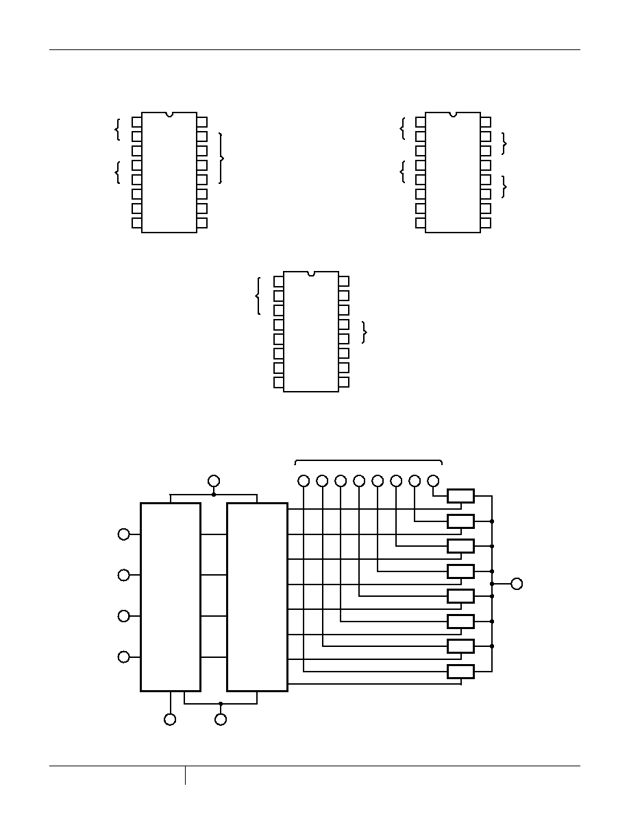
The CD4051B is a single 8-Channel multiplexer having three
binary control inputs, A, B, and C, and an inhibit input. The
three binary signals select 1 of 8 channels to be turned on,
and connect one of the 8 inputs to the output.
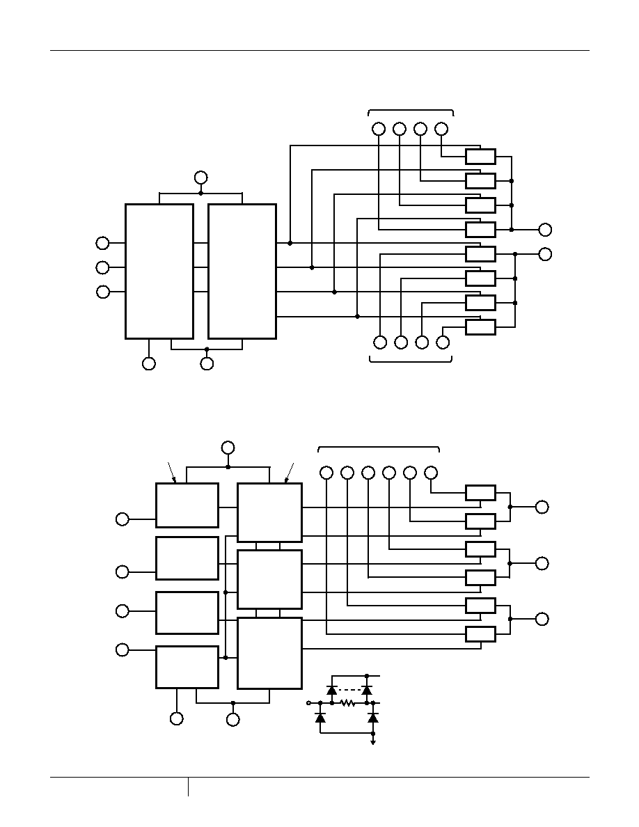
The CD4052B is a differential 4-Channel multiplexer having
two binary control inputs, A and B, and an inhibit input. The
two binary input signals select 1 of 4 pairs of channels to be
turned on and connect the analog inputs to the outputs.
The CD4053B is a triple 2-Channel multiplexer having three
separate digital control inputs, A, B, and C, and an inhibit
input. Each control input selects one of a pair of channels
which are connected in a single-pole, double-throw
configuration.
When these devices are used as demultiplexers, the
"CHANNEL IN/OUT" terminals are the outputs and the
"COMMON OUT/IN" terminals are the inputs.
NOTE: When ordering, use the entire part number. The suffixes 96
and R denote tape and reel. The suffix T denotes a small-quantity
reel of 250.
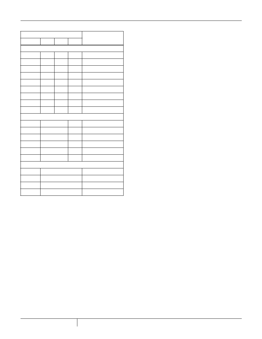
Ordering Information
PART NUMBER
TEMP. RANGE
(
o
C)
PACKAGE
CD4051BF3A, CD4052BF3A,
CD4053BF3A
-55 to 125
16 Ld CERAMIC
DIP
CD4051BE, CD4052BE,
CD4053BE
-55 to 125
16 Ld PDIP
CD4051BM, CD4051BMT,
CD4051BM96
CD4052BM, CD4052BMT,
CD4052BM96
CD4053BM, CD4053BMT,
CD4053BM96
-55 to 125
16 Ld SOIC
CD4051BNSR, CD4052BNSR,
CD4053BNSR
-55 to 125
16 Ld SOP
CD4051BPW, CD4051BPWR,
CD4052BPW, CD4052BPWR
CD4053BPW, CD4053BPWR
-55 to 125
16 Ld TSSOP
August 1998 - Revised October 2003
[ /Title
(CD405
1B,
CD4052
B,
CD4053
B)
/Sub-
ject
(CMOS
Analog
Multi-
plex-
ers/Dem
ultiplex-
ers with
Logic
Level
Conver-
sion)
/Author
()
/Key-
words
(Harris
Semi-
conduc-
tor,
CD4000
5
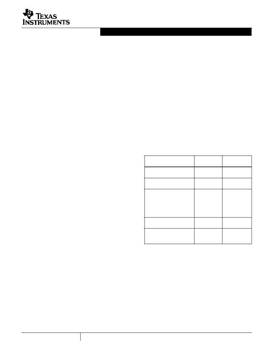
Absolute Maximum Ratings
Thermal Information
Supply Voltage (V+ to V-)
Voltages Referenced to V
SS
Terminal . . . . . . . . . . . -0.5V to 20V
DC Input Voltage Range . . . . . . . . . . . . . . . . . . -0.5V to V
DD
+0.5V
DC Input Current, Any One Input. . . . . . . . . . . . . . . . . . . . . .
±
10mA
Operating Conditions
Temperature Range . . . . . . . . . . . . . . . . . . . . . . . . . -55
o
C to 125
o
C
Package Thermal Impedance,
JA
(see Note 1):
E (PDIP) package. . . . . . . . . . . . . . . . . . . . . . . . . . . . . . . 67
o
C/W
M (SOIC) package . . . . . . . . . . . . . . . . . . . . . . . . . . . . . . 73
o
C/W
NS (SOP) package. . . . . . . . . . . . . . . . . . . . . . . . . . . . . . 64
o
C/W
PW (TSSOP) package . . . . . . . . . . . . . . . . . . . . . . . . . . 108
o
C/W
Maximum Junction Temperature (Ceramic Package) . . . . . . . . .175
o
C
Maximum Junction Temperature (Plastic Package) . . . . . . . .150
o
C
Maximum Storage Temperature Range . . . . . . . . . . -65
o
C to 150
o
C
Maximum Lead Temperature (Soldering 10s) . . . . . . . . . . . . .265
o
C
(SOIC - Lead Tips Only)
CAUTION: Stresses above those listed in "Absolute Maximum Ratings" may cause permanent damage to the device. This is a stress only rating and operation of the
device at these or any other conditions above those indicated in the operational sections of this specification is not implied.
NOTE:
1. The package thermal impedance is calculated in accordance with JESD 51-7.
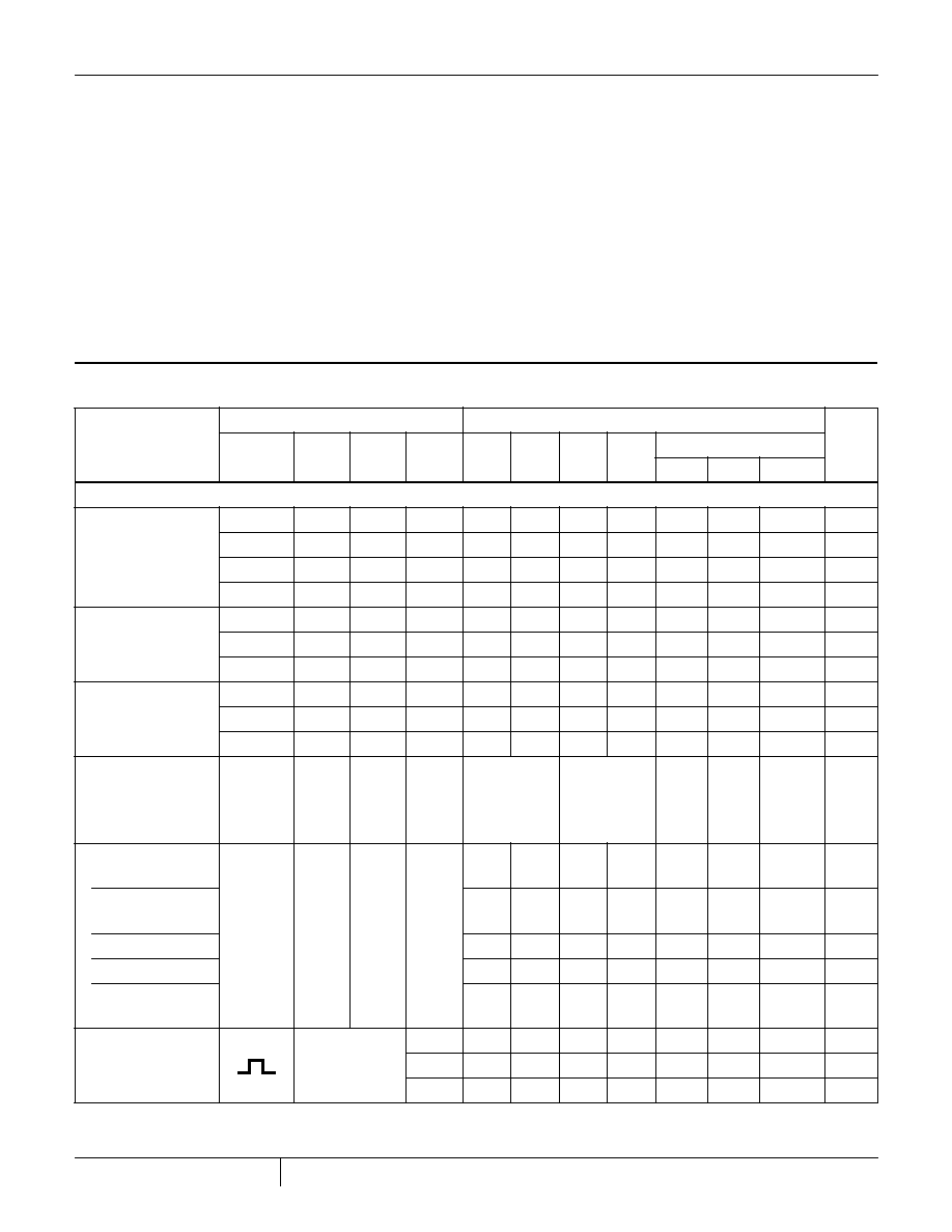
Electrical Specifications
Common Conditions Here: If Whole Table is For the Full Temp. Range, V
SUPPLY
=
±
5V, A
V
= +1,
R
L
= 100
, Unless Otherwise Specified
(Note 3)
PARAMETER
CONDITIONS
LIMITS AT INDICATED TEMPERATURES (
o
C)
UNITS
V
IS
(V)
V
EE
(V)
V
SS
(V)
V
DD
(V)
-55
-40
85
125
25
MIN
TYP
MAX
SIGNAL INPUTS (V
IS
) AND OUTPUTS (V
OS
)
Quiescent Device
Current, I
DD
Max
-
-
-
5
5
5
150
150
-
0.04
5
µ
A
-
-
-
10
10
10
300
300
-
0.04
10
µ
A
-
-
-
15
20
20
600
600
-
0.04
20
µ
A
-
-
-
20
100
100
3000
3000
-
0.08
100
µ
A
Drain to Source ON
Resistance r
ON
Max
0
V
IS
V
DD
-
0
0
5
800
850
1200
1300
-
470
1050
-
0
0
10
310
330
520
550
-
180
400
-
0
0
15
200
210
300
320
-
125
240
Change in ON
Resistance (Between
Any Two Channels),
r
ON
-
0
0
5
-
-
-
-
-
15
-
-
0
0
10
-
-
-
-
-
10
-
-
0
0
15
-
-
-
-
-
5
-
OFF Channel Leakage
Current: Any Channel
OFF (Max) or ALL
Channels OFF (Common
OUT/IN) (Max)
-
0
0
18
±
100 (Note 2)
±
1000 (Note 2)
-
±
0.01
±
100
(Note 2)
nA
Capacitance:
-
-5
5-
5
Input, C
IS
-
-
-
-
-
5
-
pF
Output, C
OS
CD4051
-
-
-
-
-
30
-
pF
CD4052
-
-
-
-
-
18
-
pF
CD4053
-
-
-
-
-
9
-
pF
Feedthrough
C
IOS
-
-
-
-
-
0.2
-
pF
Propagation Delay Time
(Signal Input to Output
V
DD
R
L
= 200k
,
C
L
= 50pF,
t
r
, t
f
= 20ns
5
-
-
-
-
-
30
60
ns
10
-
-
-
-
-
15
30
ns
15
-
-
-
-
-
10
20
ns
CD4051B, CD4052B, CD4053B