ƒÓÍÛÏÂÌÚýˆËˇ Ë ÓÔËÒýÌˡ www.docs.chipfind.ru
CD4051B Q1, CD4052B Q1, CD4053B Q1
CMOS ANALOG MULTIPLEXERS/DEMULTIPLEXERS
WITH LOGIC-LEVEL CONVERSION
SCHS354 - AUGUST 2004
1
POST OFFICE BOX 655303
∑
DALLAS, TEXAS 75265
Features
D
Qualification in Accordance With
AEC-Q100
D
Qualified for Automotive Applications
D
Customer-Specific Configuration Control
Can Be Supported Along With
Major-Change Approval
D
Wide Range of Digital and Analog Signal
Levels
- Digital: 3 V to 20 V
- Analog:
3
20 V
P-P
D
Low ON Resistance, 125
(Typ) Over
15 V
P-P
Signal Input Range
for V
DD
- V
EE
= 18 V
D
High OFF Resistance, Channel Leakage of
+
100 pA (Typ) at V
DD
- V
EE
= 18 V
D
Logic-Level Conversion for Digital
Addressing Signals of 3 V to 20 V
(V
DD
- V
SS
= 3 V to 20 V) to Switch Analog
Signals to 20 V
P-P
(V
DD
- V
EE
= 20 V)
Contact factory for details. Q100 qualification data available on
request.
D
Matched Switching Characteristics,
r
on
= 5
(Typ) for V
DD
- V
EE
= 15 V
D
Very Low Quiescent Power Dissipation
Under All Digital-Control Input and Supply
Conditions, 0.2
µ
W (Typ)
at V
DD
- V
SS
= V
DD
- V
EE
= 10 V
D
Binary Address Decoding on Chip
D
5-V, 10-V, and 15-V Parametric Ratings
D
100% Tested for Quiescent Current at 20 V
D
Maximum Input Current of 1
µ
A at 18 V Over
Full Package Temperature Range, 100 nA at
18 V and 25
∞
C
D
Break-Before-Make Switching Eliminates
Channel Overlap
Applications
D
Analog and Digital Multiplexing and
Demultiplexing
D
Analog-to-Digital (A/D) and
Digital-to-Analog (D/A) Conversion
D
Signal Gating
description/ordering information
The CD4051B, CD4052B, and CD4053B analog multiplexers are digitally-controlled analog switches that have
low ON impedance and very low OFF leakage current. Control of analog signals up to 20 V
P-P
can be achieved
by digital signal amplitudes of 4.5 V to 20 V (If V
DD
- V
SS
= 3 V, a V
DD
- V
EE
of up to 13 V can be controlled;
for V
DD
- V
EE
level differences above 13 V, a V
DD
- V
SS
of at least 4.5 V is required). For example, if
V
DD
= 4.5 V, V
SS
= 0 V, and V
EE
= -13.5 V, analog signals from -13.5 V to 4.5 V can be controlled by digital
inputs of 0 V to 5 V. These multiplexer circuits dissipate extremely low quiescent power over the full V
DD
- V
SS
and V
DD
- V
EE
supply-voltage ranges, independent of the logic state of the control signals. When a logic high
(H) is present at the inhibit (INH) input, all channels are off.
ORDERING INFORMATION
TA
PACKAGE
ORDERABLE
PART NUMBER
TOP-SIDE
MARKING
SOIC - M
Reel of 2500
CD4051BQM96Q1
CD4051Q
TSSOP - PW
Reel of 2000
CD4051BQPWRQ1
CM051BQ
-40
∞
C to 125
∞
C
SOIC - M
Reel of 2500
CD4052BQM96Q1ß
CD4052Q
-40
∞
C to 125
∞
C
TSSOP - PW
Reel of 2000
CD4052BQPWRQ1ß
CD4052Q
SOIC - M
Reel of 2500
CD4053BQM96Q1
CD4053Q
TSSOP - PW
Reel of 2000
CD4053BQPWRQ1ß
CD4053Q
Package drawings, standard packing quantities, thermal data, symbolization, and PCB design guidelines are
available at www.ti.com/sc/package.
ß Product Preview
Copyright
2004, Texas Instruments Incorporated
UNLESS OTHERWISE NOTED this document contains PRODUCTION
DATA information current as of publication date. Products conform to
specifications per the terms of Texas Instruments standard warranty.
Production processing does not necessarily include testing of all
parameters.
Please be aware that an important notice concerning availability, standard warranty, and use in critical applications of
Texas Instruments semiconductor products and disclaimers thereto appears at the end of this data sheet.
CD4051B Q1, CD4052B Q1, CD4053B Q1
CMOS ANALOG MULTIPLEXERS/DEMULTIPLEXERS
WITH LOGIC-LEVEL CONVERSION
SCHS354 - AUGUST 2004
2
POST OFFICE BOX 655303
∑
DALLAS, TEXAS 75265
description/ordering information (continued)
The CD4051B is a single eight-channel multiplexer that has three binary control inputs (A, B, and C) and an
inhibit input. The three binary signals select one of eight channels to be turned on and connect one of the eight
inputs to the output.
The CD4052B is a differential four-channel multiplexer that has two binary control inputs (A and B) and an inhibit
input. The two binary input signals select one of four pairs of channels to be turned on and connect the analog
inputs to the outputs.
The CD4053B is a triple two-channel multiplexer with three separate digital control inputs (A, B, and C) and an
inhibit input. Each control input selects one of a pair of channels, which are connected in a single-pole,
double-throw configuration.
When these devices are used as demultiplexers, the CHANNEL IN/OUT terminals are the outputs, and the
common (COM OUT/IN) terminals are the inputs.
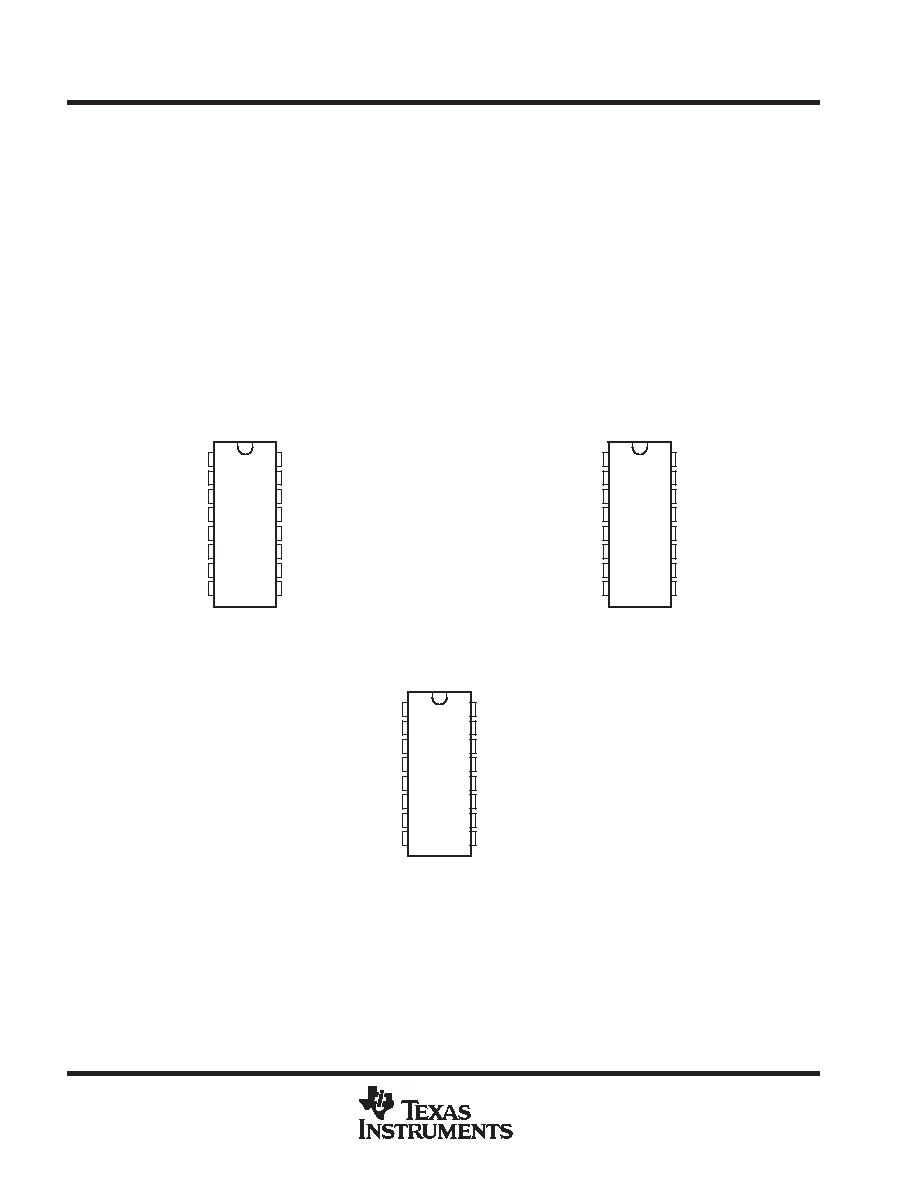
CD4053
M OR PW PACKAGE
(TOP VIEW)
1
2
3
4
5
6
7
8
16
15
14
13
12
11
10
9
IN/OUT by
IN/OUT bx
IN/OUT cy
OUT/IN CX OR CY
IN/OUT CX
INH
V
EE
V
SS
V
DD
OUT/IN bx or by
OUT/IN ax or ay
IN/OUT ay
IN/OUT ax
A
B
C
CD4051
M OR PW PACKAGE
(TOP VIEW)
1
2
3
4
5
6
7
8
16
15
14
13
12
11
10
9
CHANNEL I/O 4
CHANNEL I/O 6
COM OUT/IN
CHANNEL I/O 7
CHANNEL I/O 5
INH
V
EE
V
SS
V
DD
CHANNEL I/O 2
CHANNEL I/O 1
CHANNEL I/O 0
CHANNEL I/O 3
A
B
C
CD4052
M OR PW PACKAGE
(TOP VIEW)
1
2
3
4
5
6
7
8
16
15
14
13
12
11
10
9
Y CHANNEL I/O 0
Y CHANNEL I/O 2
COM Y OUT/IN
Y CHANNEL I/O 3
Y CHANNEL I/O 1
INH
V
EE
V
SS
V
DD
X CHANNEL I/O 2
X CHANNEL I/O 1
COM X OUT/IN
X CHANNEL I/O 0
X CHANNEL I/O 3
A
B
CD4051B Q1, CD4052B Q1, CD4053B Q1
CMOS ANALOG MULTIPLEXERS/DEMULTIPLEXERS
WITH LOGIC-LEVEL CONVERSION
SCHS354 - AUGUST 2004
3
POST OFFICE BOX 655303
∑
DALLAS, TEXAS 75265
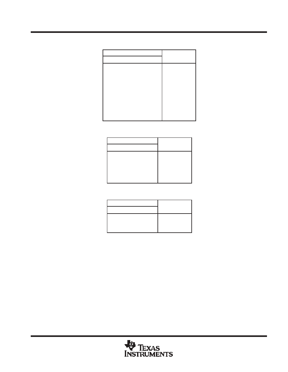
Function Tables
CD4051
INPUTS
ON
INH
C
B
A
ON
CHANNEL
L
L
L
L
0
L
L
L
H
1
L
L
H
L
2
L
L
H
H
3
L
H
L
L
4
L
H
L
H
5
L
H
H
L
6
L
H
H
H
7
H
X
X
X
None
X = don't care
CD4052
INPUTS
ON
INH
B
A
ON
CHANNEL
L
L
L
0x, 0y
L
L
H
1x, 2y
L
H
L
2x, 2y
L
H
H
3x, 3y
H
X
X
None
X = don't care
CD4053
INPUTS
ON
INH
A OR B OR C
ON
CHANNEL
L
L
ax or bx or cx
L
H
ay or by or cy
H
X
None
X = don't care
CD4051B Q1, CD4052B Q1, CD4053B Q1
CMOS ANALOG MULTIPLEXERS/DEMULTIPLEXERS
WITH LOGIC-LEVEL CONVERSION
SCHS354 - AUGUST 2004
4
POST OFFICE BOX 655303
∑
DALLAS, TEXAS 75265
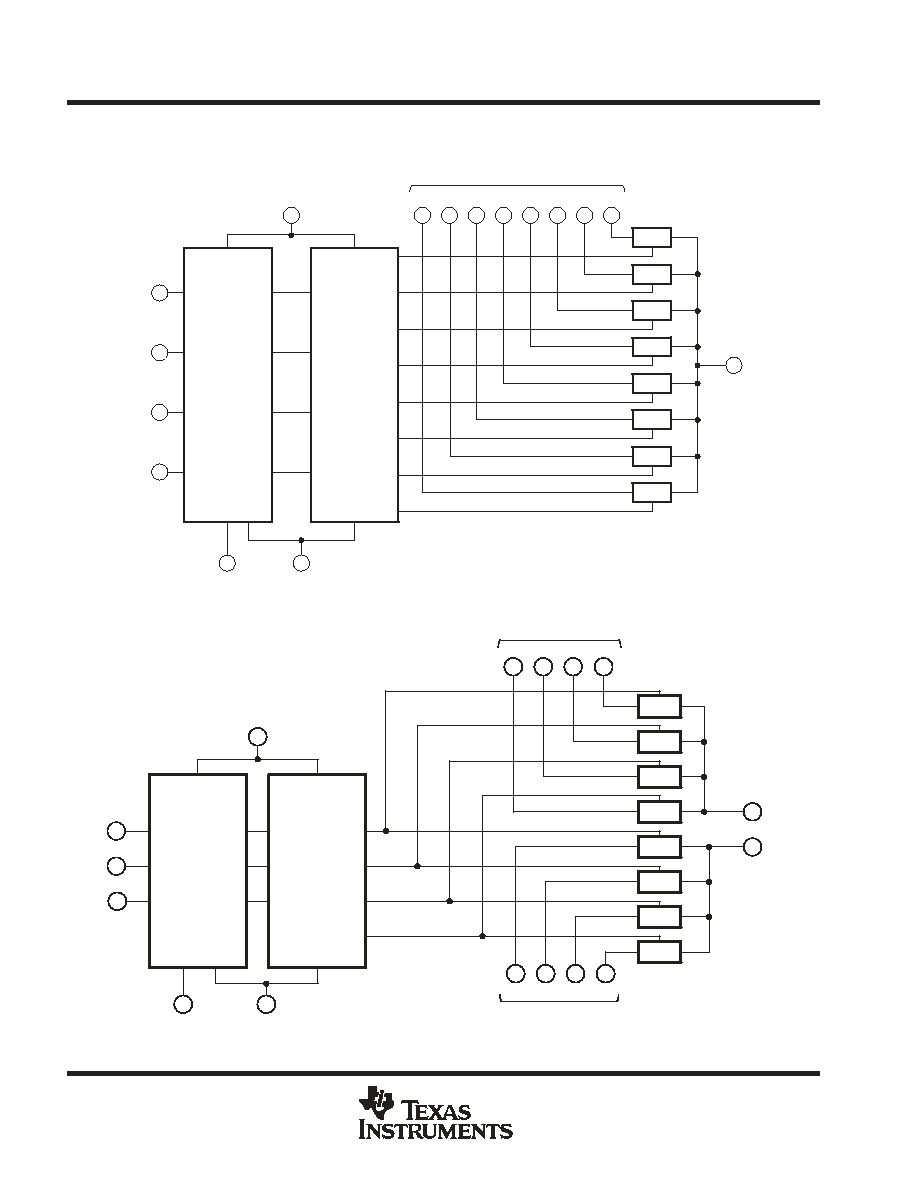
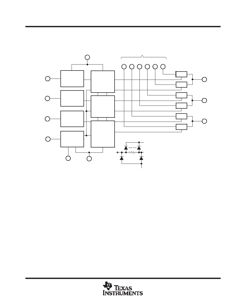
logic diagram (positive logic)
All inputs are protected by CMOS protection network.
11
10
9
6
A
B
C
INH
13
4
2
5
1
12
15
14
TG
TG
TG
TG
TG
TG
TG
TG
3
COM
OUT/IN
0
1
2
3
4
5
6
7
8
7
16
CHANNEL I/O
CD4051B
Logic-Level
Conversion
Binary
to
1-of-8
Decoder
With
Inhibit
VDD
VSS
VEE
All inputs are protected by CMOS protection network.
CD4052B
12
11
15
14
0
1
2
3
3
2
1
0
X CHANNEL I/O
Y CHANNEL I/O
13
3
7
8
16
6
9
10
A
B
INH
TG
TG
TG
TG
TG
TG
TG
TG
4
2
5
1
Binary
to
1-of-4
Decoder
With
Inhibit
COM X
OUT/IN
Logic-Level
Conversion
VDD
VSS
VEE
COM Y
OUT/IN
CD4051B Q1, CD4052B Q1, CD4053B Q1
CMOS ANALOG MULTIPLEXERS/DEMULTIPLEXERS
WITH LOGIC-LEVEL CONVERSION
SCHS354 - AUGUST 2004
5
POST OFFICE BOX 655303
∑
DALLAS, TEXAS 75265
logic diagrams (positive logic) (continued)
11
10
9
6
A
B
C
INH
12
3
5
1
2
13
TG
TG
TG
TG
TG
TG
4
ax
ay
bx
by
cx
cy
8
7
16
IN/OUT
15
14
VDD
All inputs are protected by standard CMOS protection network.
CD4053B
Logic-Level
Conversion
VDD
VSS
VEE
Binary to
1-of-2
Decoders
With
Inhibit
COM OUT/IN
ac or ay
COM OUT/IN
bc or by
COM OUT/IN
xc or xy
absolute maximum ratings over operating free-air temperature (unless otherwise noted)
Supply voltage range, V+ to V- (voltages referenced to V
SS
terminal)
-0.5 to 20 V
. . . . . . . . . . . . . . . . . . . . .
DC input voltage range
-0.5 V to V
DD
+ 0.5 V
. . . . . . . . . . . . . . . . . . . . . . . . . . . . . . . . . . . . . . . . . . . . . . . . . . . . . .
DC input current, any one input
±
10 mA
. . . . . . . . . . . . . . . . . . . . . . . . . . . . . . . . . . . . . . . . . . . . . . . . . . . . . . . . . . .
Package thermal impedance,
JA
(see Note 1): M package
73
∞
C/W
. . . . . . . . . . . . . . . . . . . . . . . . . . . . . . . . . .
PW package
108
∞
C/W
. . . . . . . . . . . . . . . . . . . . . . . . . . . . . . . .
Maximum junction temperature, T
J
150
∞
C
. . . . . . . . . . . . . . . . . . . . . . . . . . . . . . . . . . . . . . . . . . . . . . . . . . . . . . . . .
Lead temperature (during soldering):
At distance 1/16
±
1/32 inch (1,59
±
0,79 mm) from case for 10 s max
265
∞
C
. . . . . . . . . . . . . . . . . . . . . . .
Storage temperature range, T
stg
-65
∞
C to 150
∞
C
. . . . . . . . . . . . . . . . . . . . . . . . . . . . . . . . . . . . . . . . . . . . . . . . . . .
Stresses beyond those listed under "absolute maximum ratings" may cause permanent damage to the device. These are stress ratings only, and
functional operation of the device at these or any other conditions beyond those indicated under "recommended operating conditions" is not
implied. Exposure to absolute-maximum-rated conditions for extended periods may affect device reliability.
NOTE 1: The package thermal impedance is calculated in accordance with JESD 51-7.