CD54AC161, CD74AC161
4-BIT SYNCHRONOUS BINARY COUNTERS
SCHS239C ≠ SEPTEMBER 1998 ≠ REVISED MARCH 2003
1
POST OFFICE BOX 655303
∑
DALLAS, TEXAS 75265
D
Internal Look-Ahead for Fast Counting
D
Carry Output for n-Bit Cascading
D
Synchronous Counting
D
Synchronously Programmable
D
SCR-Latchup-Resistant CMOS Process and
Circuit Design
D
Exceeds 2-kV ESD Protection per
MIL-STD-883, Method 3015
description/ordering information
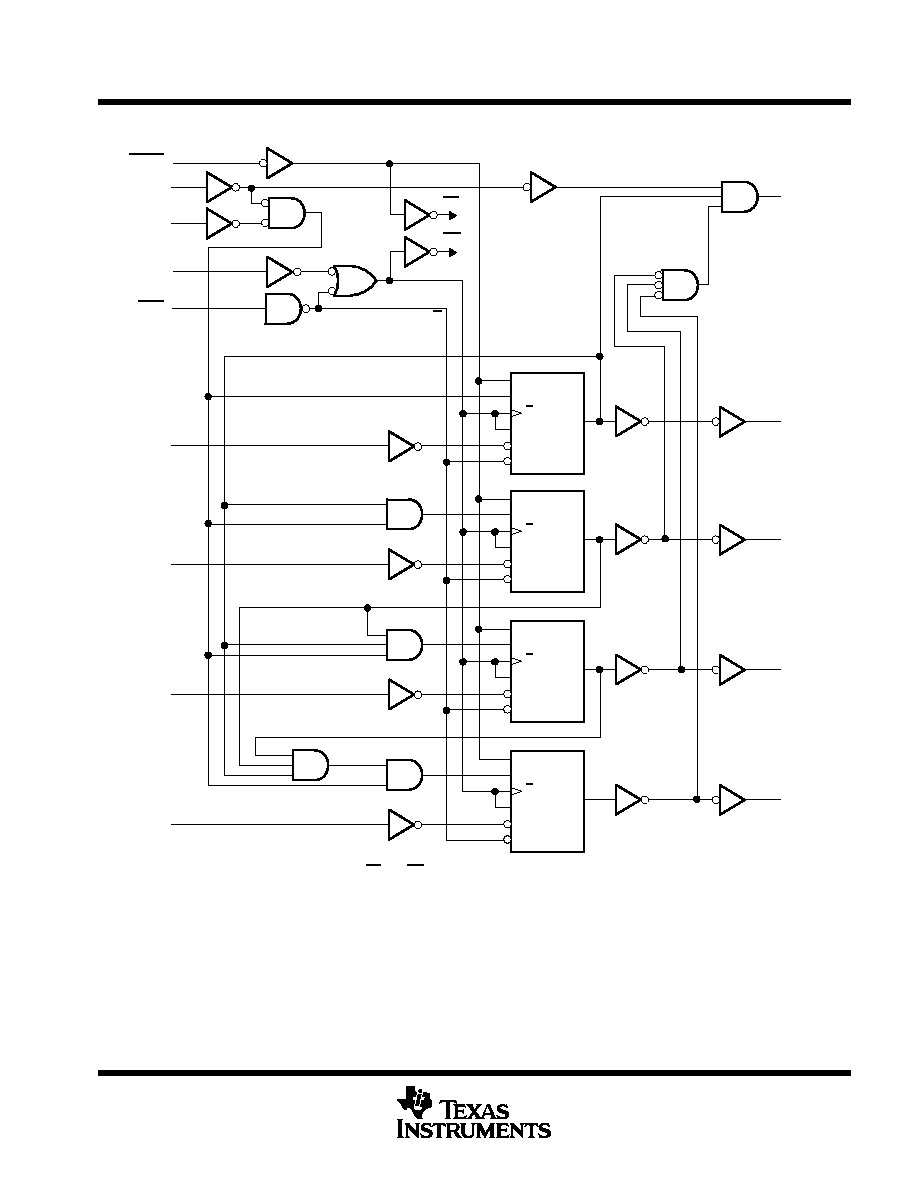
The 'AC161 devices are 4-bit binary counters.
These synchronous, presettable counters feature
an internal carry look-ahead for application in
high-speed counting These devices are fully programmable; that is, they can be preset to any number between
0 and 9 or 15. Presetting is synchronous; therefore, setting up a low level at the load input disables the counter
and causes the outputs to agree with the setup data after the next clock pulse, regardless of the levels of the
enable inputs.
The clear function is asynchronous. A low level at the clear (CLR) input sets all four of the flip-flop outputs low,
regardless of the levels of the CLK, load (LOAD), or enable inputs.
The carry look-ahead circuitry provides for cascading counters for n-bit synchronous applications without
additional gating. Instrumental in accomplishing this function are ENP, ENT, and a ripple-carry output (RCO).
Both ENP and ENT must be high to count, and ENT is fed forward to enable RCO. Enabling RCO produces a
high-level pulse while the count is maximum (9 or 15, with Q
A
high). This high-level overflow ripple-carry pulse
can be used to enable successive cascaded stages. Transitions at ENP or ENT are allowed, regardless of the
level of CLK.
The counters feature a fully independent clock circuit. Changes at control inputs (ENP, ENT, or LOAD) that
modify the operating mode have no effect on the contents of the counter until clocking occurs. The function of
the counter (whether enabled, disabled, loading, or counting) is dictated solely by the conditions meeting the
stable setup and hold times.
ORDERING INFORMATION
TA
PACKAGE
ORDERABLE
PART NUMBER
TOP-SIDE
MARKING
PDIP ≠ E
Tube
CD74AC161E
CD74AC161E
55
∞
C to 125
∞
C
SOIC
M
Tube
CD74AC161M
AC161M
≠55
∞
C to 125
∞
C
SOIC ≠ M
Tape and reel
CD74AC161M96
AC161M
CDIP ≠ F
Tube
CD54AC161F3A
CD54AC161F3A
Package drawings, standard packing quantities, thermal data, symbolization, and PCB
design guidelines are available at www.ti.com/sc/package.
Please be aware that an important notice concerning availability, standard warranty, and use in critical applications of
Texas Instruments semiconductor products and disclaimers thereto appears at the end of this data sheet.
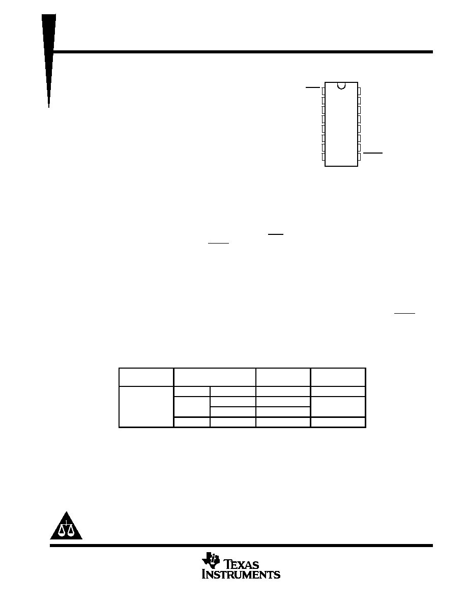
1
2
3
4
5
6
7
8
16
15
14
13
12
11
10
9
CLR
CLK
A
B
C
D
ENP
GND
V
CC
RCO
Q
A
Q
B
Q
C
Q
D
ENT
LOAD
CD54AC161 . . . F PACKAGE
CD74AC161 . . . E OR M PACKAGE
(TOP VIEW)
Copyright
2003, Texas Instruments Incorporated
PRODUCTION DATA information is current as of publication date.
Products conform to specifications per the terms of Texas Instruments
standard warranty. Production processing does not necessarily include
testing of all parameters.
On products compliant to MIL-PRF-38535, all parameters are tested
unless otherwise noted. On all other products, production
processing does not necessarily include testing of all parameters.
CD54AC161, CD74AC161
4-BIT SYNCHRONOUS BINARY COUNTERS
SCHS239C ≠ SEPTEMBER 1998 ≠ REVISED MARCH 2003
2
POST OFFICE BOX 655303
∑
DALLAS, TEXAS 75265
FUNCTION TABLE
INPUTS
OUTPUTS
FUNCTION
CLR
CLK
ENP
ENT
LOAD
A,B,C,D
Qn
RCO
FUNCTION
L
X
X
X
X
X
L
L
Reset (clear)
H
X
X
l
l
L
L
Parallel load
H
X
X
l
h
H
Note 1
Parallel load
H
h
h
h
X
Count
Note 1
Count
H
X
l
X
h
X
qn
Note 1
Inhibit
H
X
X
l
h
X
qn
L
Inhibit
H = high level, L = low level, X = don't care, h = high level one setup time prior to the CLK
low-to-high transition, l = low level one setup time prior to the CLK low-to-high transition, q = the
state of the referenced output prior to the CLK low-to-high transition, and
= CLK low-to-high
transition.
NOTE 1: The RCO output is high when ENT is high and the counter is at terminal count
(HHHH).
CD54AC161, CD74AC161
4-BIT SYNCHRONOUS BINARY COUNTERS
SCHS239C ≠ SEPTEMBER 1998 ≠ REVISED MARCH 2003
4
POST OFFICE BOX 655303
∑
DALLAS, TEXAS 75265
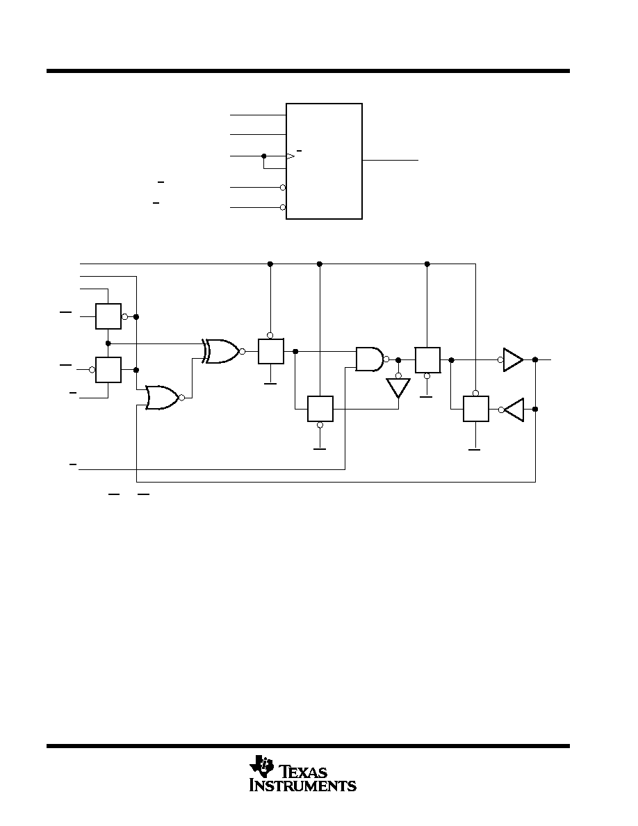
logic symbol, each D/T flip-flop
M1
LD (Load)
Q (Output)
G2
TE (Toggle Enable)
CK (Clock)
G4
3D
4R
1, 2T/1C3
D (Inverted Data)
R (Inverted Reset)
logic diagram, each D/T flip-flop (positive logic)
TG
TG
TG
TG
TG
TG
CK
LD
TE
LD
LD
D
R
CK
CK
CK
CK
Q
The origins of LD and CK are shown in the logic diagram of the overall device.
CD54AC161, CD74AC161
4-BIT SYNCHRONOUS BINARY COUNTERS
SCHS239C ≠ SEPTEMBER 1998 ≠ REVISED MARCH 2003
5
POST OFFICE BOX 655303
∑
DALLAS, TEXAS 75265
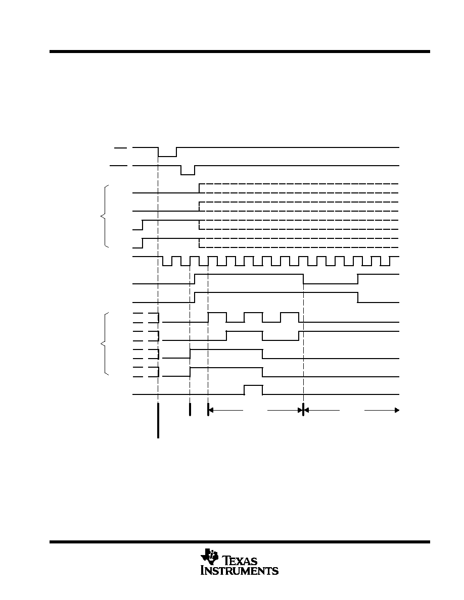
typical clear, preset, count, and inhibit sequence
The following sequence is illustrated below:
1.
Clear outputs to zero (asynchronous)
2.
Preset to binary 12
3.
Count to 13, 14, 15, 0, 1, and 2
4.
Inhibit
Data
Inputs
Data
Outputs
CLR
LOAD
A
B
C
D
CLK
ENP
ENT
RCO
QA
QB
QC
QD
Async
Clear
Preset
Count
Inhibit
12
13
14
15
0
1
2