 | –≠–ª–µ–∫—Ç—Ä–æ–Ω–Ω—ã–π –∫–æ–º–ø–æ–Ω–µ–Ω—Ç: CD54HC163 | –°–∫–∞—á–∞—Ç—å:  PDF PDF  ZIP ZIP |
1
Data sheet acquired from Harris Semiconductor
SCHS154A
Features
∑ 'HC161, 'HCT161 4-Bit Binary Counter,
Asynchronous Reset
∑ 'HC163, 'HCT163 4-Bit Binary Counter,
Synchronous Reset
∑ Synchronous Counting and Loading
∑ Two Count Enable Inputs for n-Bit Cascading
∑ Look-Ahead Carry for High-Speed Counting
∑ Fanout (Over Temperature Range)
- Standard Outputs . . . . . . . . . . . . . . . 10 LSTTL Loads
- Bus Driver Outputs . . . . . . . . . . . . . 15 LSTTL Loads
∑ Wide Operating Temperature Range . . . -55
o
C to 125
o
C
∑ Balanced Propagation Delay and Transition Times
∑ Significant Power Reduction Compared to LSTTL
Logic ICs
∑ HC Types
- 2V to 6V Operation
- High Noise Immunity: N
IL
= 30%, N
IH
= 30% of V
CC
at V
CC
= 5V
∑ HCT Types
- 4.5V to 5.5V Operation
- Direct LSTTL Input Logic Compatibility,
V
IL
= 0.8V (Max), V
IH
= 2V (Min)
- CMOS Input Compatibility, I
l
1
µ
A at V
OL
, V
OH
Description
The
'HC161,
'HCT161,
'HC163,
and
'HCT163
are
presettable synchronous counters that feature look-ahead
carry logic for use in high-speed counting applications. The
'HC161 and 'HCT161 are asynchronous reset decade and
binary counters, respectively; the 'HC163 and 'HCT163
devices are decade and binary counters, respectively, that
are reset synchronously with the clock. Counting and
parallel presetting are both accomplished synchronously
with the negative-to-positive transition of the clock.
A low level on the synchronous parallel enable input, SPE,
disables counting operation and allows data at the P0 to P3
inputs to be loaded into the counter (provided that the
setup and hold requirements for SPE are met).
All counters are reset with a low level on the Master Reset
input,
MR.
In
the
'HC163
and
'HCT163
counters
(synchronous reset types), the requirements for setup and
hold time with respect to the clock must be met.
Two count enables, PE and TE, in each counter are
provided for n-bit cascading. In all counters reset action
occurs regardless of the level of the SPE, PE and TE inputs
(and the clock input, CP, in the 'HC161 and 'HCT161
types).
If a decade counter is preset to an illegal state or assumes
an illegal state when power is applied, it will return to the
normal sequence in one count as shown in state diagram.
The look-ahead carry feature simplifies serial cascading of
the counters. Both count enable inputs (PE and TE) must
be high to count. The TE input is gated with the Q outputs
of all four stages so that at the maximum count the terminal
count (TC) output goes high for one clock period. This TC
pulse is used to enable the next cascaded stage.
Ordering Information
PART NUMBER
TEMP. RANGE
(
o
C)
PACKAGE
CD54HC161F
-55 to 125
16 Ld CERDIP
CD54HC161F3A
-55 to 125
16 Ld CERDIP
CD74HC161E
-55 to 125
16 Ld PDIP
CD74HC161M
-55 to 125
16 Ld SOIC
CD54HCT161F3A
-55 to 125
16 Ld CERDIP
CD74HCT161E
-55 to 125
16 Ld PDIP
CD74HCT161M
-55 to 125
16 Ld SOIC
CD54HC163F3A
-55 to 125
16 Ld CERDIP
CD74HC163E
-55 to 125
16 Ld PDIP
CD74HC163M
-55 to 125
16 Ld SOIC
CD54HCT163F
-55 to 125
16 Ld CERDIP
CD54HCT163F3A
-55 to 125
16 Ld CERDIP
CD74HCT163E
-55 to 125
16 Ld PDIP
CD74HCT163M
-55 to 125
16 Ld SOIC
NOTES:
1. When ordering, use the entire part number. Add the suffix 96 to ob-
tain the variant in the tape and reel.
2. Wafer and die for this part number is available which meets all elec-
trical specifications. Please contact your local TI sales office or cus-
tomer service for ordering information.
February 1998 - Revised May 2000
CAUTION: These devices are sensitive to electrostatic discharge. Users should follow proper IC Handling Procedures.
Copyright
©
2000, Texas Instruments Incorporated
CD54/74HC161, CD54/74HCT161,
CD54/74HC163, CD54/74HCT163
High Speed CMOS Logic
Presettable Counters
[ /Title
(CD74
HC161
,
CD74
HCT16
1,
CD74
HC163
,
CD74
HCT16
3)
/Sub-
ject
(High
Speed
CMOS
Logic
Preset-
table
Counte
rs)
/Autho
r ()
/Key-
words
(High
Speed
CMOS
Logic
Preset-
table
Counte
rs,
High
Speed
2
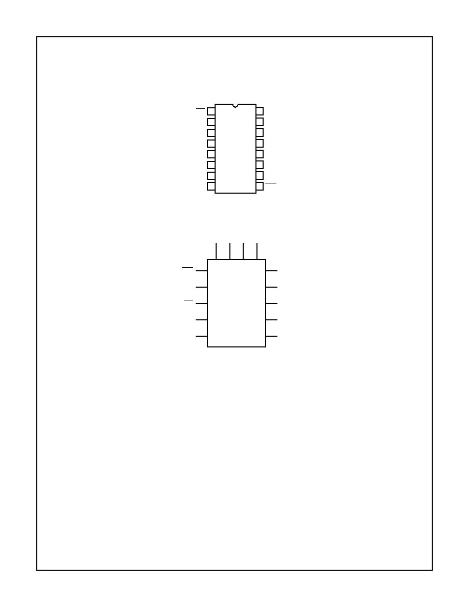
Pinout
CD54HC161, CD54HCT161, CD54HC163, CD54HCT163
(CERDIP)
CD74HC161, CD74HCT161, CD74HC163, CD74HCT163
(PDIP, SOIC)
TOP VIEW
Functional Diagram
14
15
16
9
13
12
11
10
1
2
3
4
5
7
6
8
MR
CP
P0
P1
P2
P3
GND
PE
V
CC
Q0
Q1
Q2
Q3
TE
SPE
TC
SPE
CP
MR
PE
TE
9
2
1
7
10
3
4
5
6
14
13
12
11
15
Q0
Q1
Q2
Q3
TC
P0
P1
P2
P3
CD54/74HC161, CD54/74HCT161, CD54/74HC163, CD54/74HCT163

3
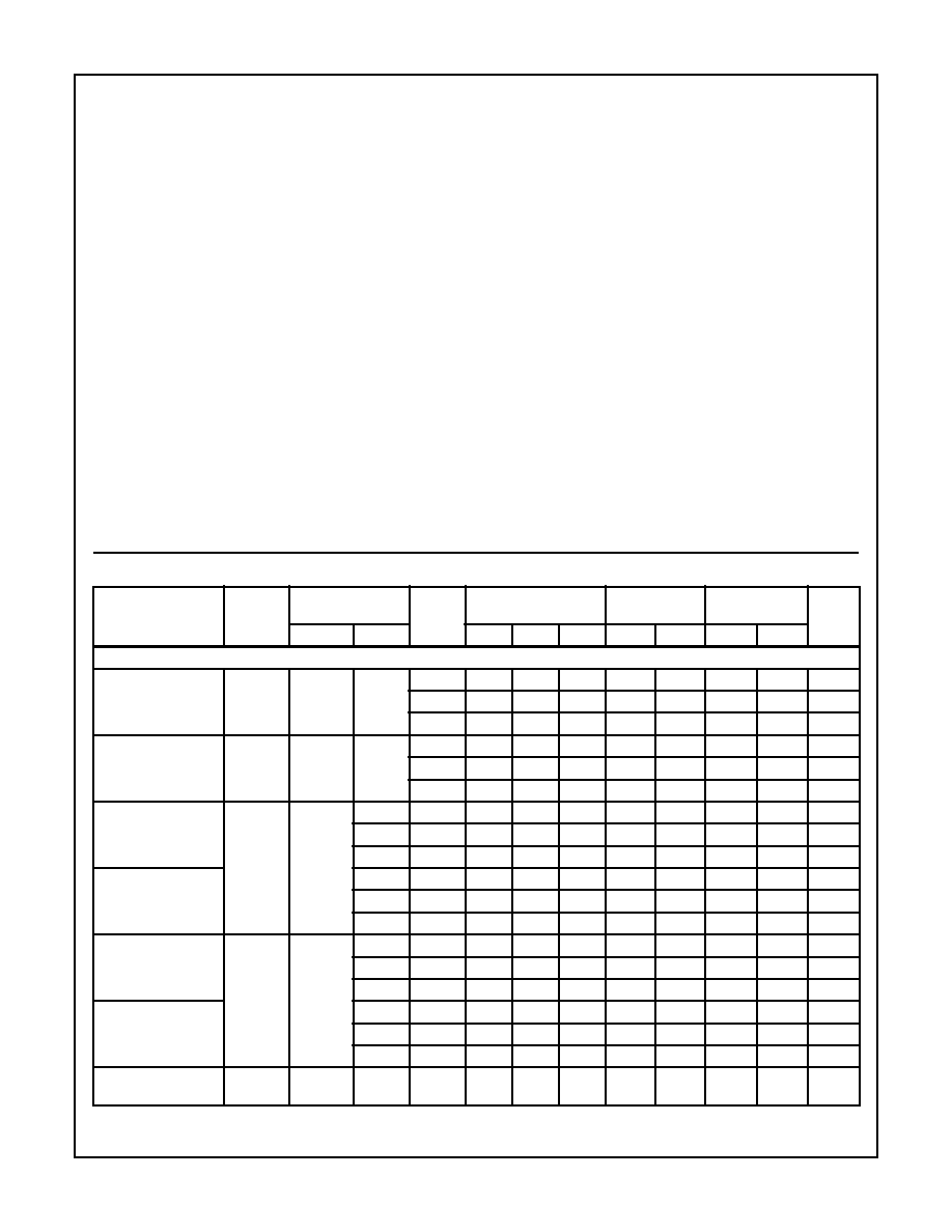
MODE SELECT - FUNCTION TABLE FOR 'HC161 AND 'HCT161
OPERATING MODE
INPUTS
OUTPUTS
MR
CP
PE
TE
SPE
P
n
Q
n
TC
Reset (Clear)
L
X
X
X
X
X
L
L
Parallel Load
H
X
X
l
l
L
L
H
X
X
l
h
H
(Note 3)
Count
H
h
h
h (Note 5)
X
Count
(Note 3)
Inhibit
H
X
I (Note 4)
X
h (Note 5)
X
q
n
(Note 3)
H
X
X
I (Note 4)
h (Note 5)
X
q
n
L
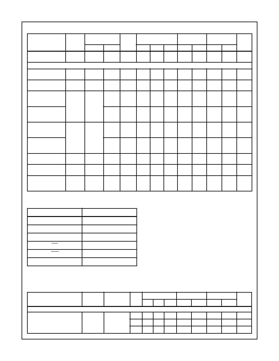
MODE SELECT - FUNCTION TABLE FOR 'HC163 AND 'HCT163
OPERATING MODE
INPUTS
OUTPUTS
MR
CP
PE
TE
SPE
P
n
Q
n
TC
Reset (Clear)
l
X
X
X
X
L
L
Parallel Load
h (Note 5)
X
X
l
l
L
L
h (Note 5)
X
X
l
h
H
(Note 3)
Count
h (Note 5)
h
h
h (Note 5)
X
Count
(Note 3)
Inhibit
h (Note 5)
X
I (Note 4)
X
h (Note 5)
X
q
n
(Note 3)
h (Note 5)
X
X
I (Note 4)
h (Note 5)
X
q
n
L
NOTE: H = High voltage level steady state; L = Low voltage level steady state; h = High voltage level one setup time prior to the Low-to-High
clock transition; l = Low voltage level one setup time prior to the Low-to-High clock transition; X = Don't Care; q = Lower case letters indicate
the state of the referenced output prior to the Low-to-High clock transition;
= Low-to-High clock transition.
3. The TC output is High when TE is High and the counter is at Terminal Count (HHHH for HC/HCT161 and 'HC/HCT163).
4. The High-to-Low transition of PE or TE on the 'HC/HCT161 and the 'HC/HCT163 should only occur while CP is HIGH for conventional
operation.
5. The Low-to-High transition of SPE on the 'HC/HCT161 and SPE or MR on the 'HC/HCT163 should only occur while CP is HIGH for con-
ventional operation.
CD54/74HC161, CD54/74HCT161, CD54/74HC163, CD54/74HCT163
4
Absolute Maximum Ratings
Thermal Information
DC Supply Voltage, V
CC
. . . . . . . . . . . . . . . . . . . . . . . . -0.5V to 7V
DC Input Diode Current, I
IK
For V
I
< -0.5V or V
I
> V
CC
+ 0.5V
. . . . . . . . . . . . . . . . . . . . . .±
20mA
DC Output Diode Current, I
OK
For V
O
< -0.5V or V
O
> V
CC
+ 0.5V
. . . . . . . . . . . . . . . . . . . .±
20mA
DC Drain Current, per Output, I
O
For -0.5V < V
O
< V
CC
+ 0.5V
. . . . . . . . . . . . . . . . . . . . . . . . . .±
25mA
DC Output Source or Sink Current per Output Pin, I
O
For V
O
> -0.5V or V
O
< V
CC
+ 0.5V
. . . . . . . . . . . . . . . . . . . .±
25mA
DC V
CC
or Ground Current, I
CC
. . . . . . . . . . . . . . . . . . . . . . . . .±
50mA
Operating Conditions
Temperature Range, T
A
. . . . . . . . . . . . . . . . . . . . . . -55
o
C to 125
o
C
Supply Voltage Range, V
CC
HC Types . . . . . . . . . . . . . . . . . . . . . . . . . . . . . . . . . . . . .2V to 6V
HCT Types . . . . . . . . . . . . . . . . . . . . . . . . . . . . . . . . .4.5V to 5.5V
DC Input or Output Voltage, V
I
, V
O
. . . . . . . . . . . . . . . . . 0V to V
CC
Input Rise and Fall Time
2V . . . . . . . . . . . . . . . . . . . . . . . . . . . . . . . . . . . . . . 1000ns (Max)
4.5V. . . . . . . . . . . . . . . . . . . . . . . . . . . . . . . . . . . . . . 500ns (Max)
6V . . . . . . . . . . . . . . . . . . . . . . . . . . . . . . . . . . . . . . . 400ns (Max)
Thermal Resistance (Typical, Note 6)
JA
(
o
C/W)
PDIP Package . . . . . . . . . . . . . . . . . . . . . . . . . . . . .
90
SOIC Package . . . . . . . . . . . . . . . . . . . . . . . . . . . . .
160
Maximum Junction Temperature . . . . . . . . . . . . . . . . . . . . . . . 150
o
C
Maximum Storage Temperature Range . . . . . . . . . .-65
o
C to 150
o
C
Maximum Lead Temperature (Soldering 10s) . . . . . . . . . . . . . 300
o
C
(SOIC - Lead Tips Only)
CAUTION: Stresses above those listed in "Absolute Maximum Ratings" may cause permanent damage to the device. This is a stress only rating and operation
of the device at these or any other conditions above those indicated in the operational sections of this specification is not implied.
NOTE:
6.
JA
is measured with the component mounted on an evaluation PC board in free air.
DC Electrical Specifications
PARAMETER
SYMBOL
TEST
CONDITIONS
V
CC
(V)
25
o
C
-40
o
C TO 85
o
C -55
o
C TO 125
o
C
UNITS
V
I
(V)
I
O
(mA)
MIN
TYP
MAX
MIN
MAX
MIN
MAX
HC TYPES
High Level Input
Voltage
V
IH
-
-
2
1.5
-
-
1.5
-
1.5
-
V
4.5
3.15
-
-
3.15
-
3.15
-
V
6
4.2
-
-
4.2
-
4.2
-
V
Low Level Input
Voltage
V
IL
-
-
2
-
-
0.5
-
0.5
-
0.5
V
4.5
-
-
1.35
-
1.35
-
1.35
V
6
-
-
1.8
-
1.8
-
1.8
V
High Level Output
Voltage
CMOS Loads
V
OH
V
IH
or V
IL
-0.02
2
1.9
-
-
1.9
-
1.9
-
V
-0.02
4.5
4.4
-
-
4.4
-
4.4
-
V
-0.02
6
5.9
-
-
5.9
-
5.9
-
V
High Level Output
Voltage
TTL Loads
-
-
-
-
-
-
-
-
-
V
-4
4.5
3.98
-
-
3.84
-
3.7
-
V
-5.2
6
5.48
-
-
5.34
-
5.2
-
V
Low Level Output
Voltage
CMOS Loads
V
OL
V
IH
or V
IL
0.02
2
-
-
0.1
-
0.1
-
0.1
V
0.02
4.5
-
-
0.1
-
0.1
-
0.1
V
0.02
6
-
-
0.1
-
0.1
-
0.1
V
Low Level Output
Voltage
TTL Loads
-
-
-
-
-
-
-
-
-
V
4
4.5
-
-
0.26
-
0.33
-
0.4
V
5.2
6
-
-
0.26
-
0.33
-
0.4
V
Input Leakage
Current
I
I
V
CC
or
GND
-
6
-
-
±
0.1
-
±
1
-
±
1
µ
A
CD54/74HC161, CD54/74HCT161, CD54/74HC163, CD54/74HCT163
5
Quiescent Device
Current
I
CC
V
CC
or
GND
0
6
-
-
8
-
80
-
160
µ
A
HCT TYPES
High Level Input
Voltage
V
IH
-
-
4.5 to
5.5
2
-
-
2
-
2
-
V
Low Level Input
Voltage
V
IL
-
-
4.5 to
5.5
-
-
0.8
-
0.8
-
0.8
V
High Level Output
Voltage
CMOS Loads
V
OH
V
IH
or V
IL
-0.02
4.5
4.4
-
-
4.4
-
4.4
-
V
High Level Output
Voltage
TTL Loads
-4
4.5
3.98
-
-
3.84
-
3.7
-
V
Low Level Output
Voltage
CMOS Loads
V
OL
V
IH
or V
IL
0.02
4.5
-
-
0.1
-
0.1
-
0.1
V
Low Level Output
Voltage
TTL Loads
4
4.5
-
-
0.26
-
0.33
-
0.4
V
Input Leakage
Current
I
I
V
CC
and
GND
0
5.5
-
±
0.1
-
±
1
-
±
1
µ
A
Quiescent Device
Current
I
CC
V
CC
or
GND
0
5.5
-
-
8
-
80
-
160
µ
A
Additional Quiescent
Device Current Per
Input Pin: 1 Unit Load
I
CC
(Note)
V
CC
-2.1
-
4.5 to
5.5
-
100
360
-
450
-
490
µ
A
NOTE: For dual-supply systems theoretical worst case (V
I
= 2.4V, V
CC
= 5.5V) specification is 1.8mA.
DC Electrical Specifications
(Continued)
PARAMETER
SYMBOL
TEST
CONDITIONS
V
CC
(V)
25
o
C
-40
o
C TO 85
o
C -55
o
C TO 125
o
C
UNITS
V
I
(V)
I
O
(mA)
MIN
TYP
MAX
MIN
MAX
MIN
MAX
HCT Input Loading Table
INPUT
UNIT LOADS
P0 - P3
0.25
PE
0.65
CP
1.05
MR
0.8
SPE
0.5
TE
1.05
NOTE: Unit Load is
I
CC
limit specified in DC Electrical Table, e.g.,
360
µ
A max at 25
o
C.
Prerequisite For Switching Specifications
PARAMETER
SYMBOL
TEST
CONDITIONS
V
CC
(V)
25
o
C
-40
o
C TO 85
o
C
-55
o
C TO 125
o
C
UNITS
MIN
TYP
MAX
MIN
MAX
MIN
MAX
HC TYPES
Maximum CP Frequency
(Note7)
f
MAX
-
2
6
-
-
5
-
4
-
MHz
4.5
30
-
-
24
-
20
-
MHz
6
35
-
-
28
-
24
-
MHz
CD54/74HC161, CD54/74HCT161, CD54/74HC163, CD54/74HCT163