CD54HC4017
DECADE COUNTER/DIVIDER
WITH TEN DECODED OUTPUTS
SGDS011 ≠ MAY 1999
1
POST OFFICE BOX 655303
∑
DALLAS, TEXAS 75265
D
2-V to 6-V Operation
D
Fully Static Operation
D
Buffered Inputs
D
Common Reset
D
Positive-Edge Clocking
D
Balanced Propagation Delay and Transition
Times
D
High Noise Immunity: N
IL
= 30%, N
IH
= 30%
of V
CC
at V
CC
= 5 V
D
Packaged in Ceramic (F) DIP Package and
Also Available in Chip Form (H)
description
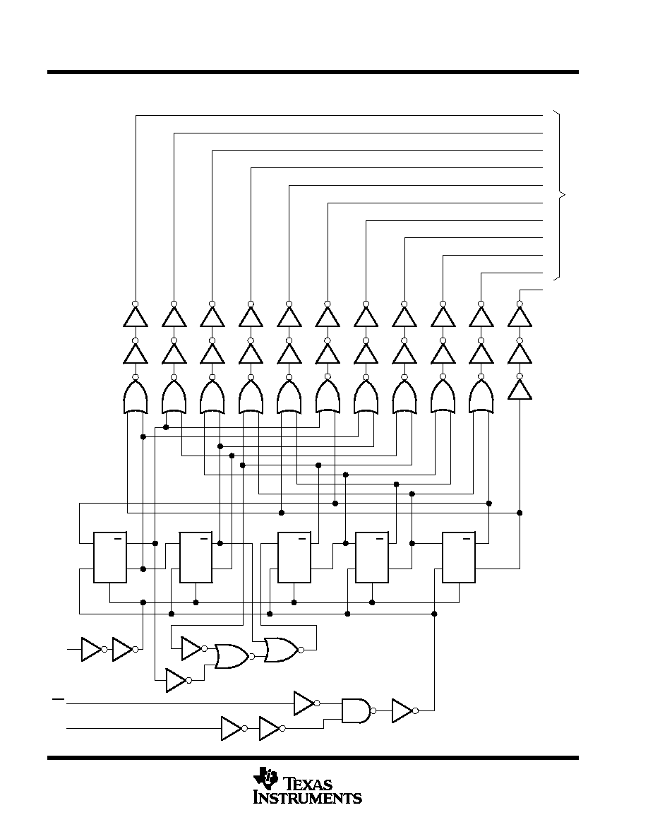
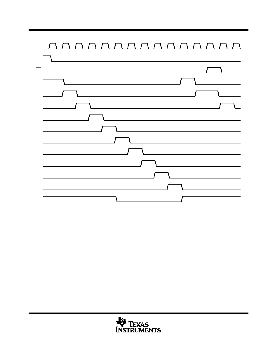
The CD54HC4017 is a high-speed silicon-gate CMOS 5-stage Johnson counter with ten decoded outputs. Each
decoded output normally is low and sequentially goes high on the low-to-high transition of the clock (CP) input.
Each output stays high for one clock period of the ten-clock-period cycle. The terminal count (TC) output
transitions low to high after output ten (9) goes low, and can be used in conjunction with the clock enable (CE)
input to cascade several stages. CE disables counting when in the high state. The master reset (MR) input, when
taken high, sets all the decoded outputs, except 0, to low.
The CD54HC4017 is characterized for operation over the full military temperature range of ≠55
∞
C to 125
∞
C.
FUNCTION TABLE
INPUTS
OUTPUT STATE
CP
CE
MR
OUTPUT STATE
L
X
L
No change
X
H
L
No change
X
X
H
0 = H
1≠9 = L
L
L
Increments counter
X
L
No change
X
L
No change
H
L
Increments counter
If n < 5, TC = H; otherwise, TC = L.
Copyright
©
1999, Texas Instruments Incorporated
PRODUCTION DATA information is current as of publication date.
Products conform to specifications per the terms of Texas Instruments
standard warranty. Production processing does not necessarily include
testing of all parameters.
Please be aware that an important notice concerning availability, standard warranty, and use in critical applications of
Texas Instruments semiconductor products and disclaimers thereto appears at the end of this data sheet.
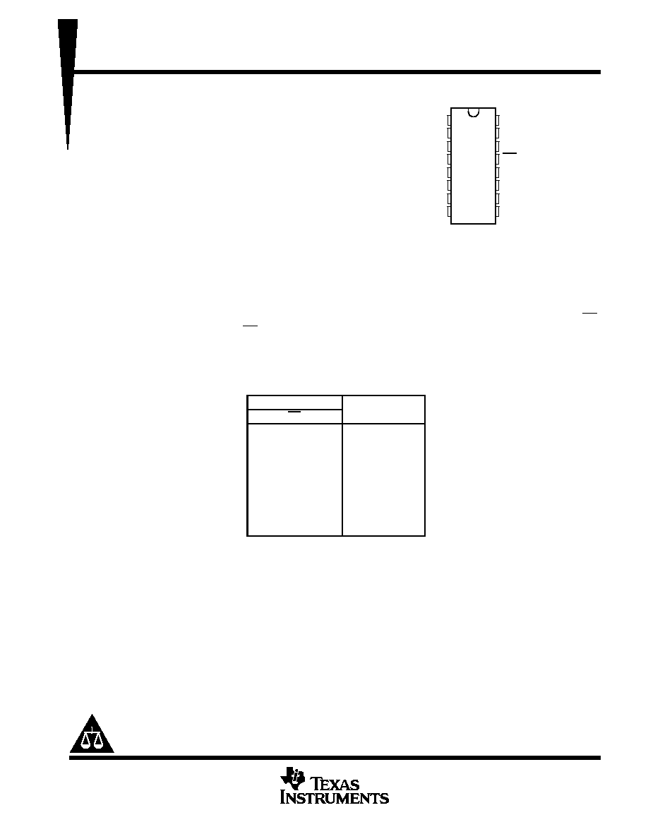
1
2
3
4
5
6
7
8
16
15
14
13
12
11
10
9
5
1
0
2
6
7
3
GND
V
CC
MR
CP
CE
TC
9
4
8
F PACKAGE
(TOP VIEW)
CD54HC4017
DECADE COUNTER/DIVIDER
WITH TEN DECODED OUTPUTS
SGDS011 ≠ MAY 1999
3
POST OFFICE BOX 655303
∑
DALLAS, TEXAS 75265
absolute maximum ratings over operating free-air temperature (unless otherwise noted)
Supply voltage range, V
CC
≠0.5 V to 7 V
. . . . . . . . . . . . . . . . . . . . . . . . . . . . . . . . . . . . . . . . . . . . . . . . . . . . . . . . . .
Input clamp current, I
IK
(V
I
< 0 V or V
I
> V
CC
)
±
20 mA
. . . . . . . . . . . . . . . . . . . . . . . . . . . . . . . . . . . . . . . . . . . . . .
Output clamp current, I
OK
(V
O
< 0 V or V
O
> V
CC
)
±
20 mA
. . . . . . . . . . . . . . . . . . . . . . . . . . . . . . . . . . . . . . . . . .
Continuous output current, each output pin, I
O
(V
O
> ≠0.5 V or V
O
< V
CC
+ 0.5 V)
±
25 mA
. . . . . . . . . . . . . .
V
CC
or ground current, I
CC
±
50 mA
. . . . . . . . . . . . . . . . . . . . . . . . . . . . . . . . . . . . . . . . . . . . . . . . . . . . . . . . . . . . . .
Storage temperature range, T
stg
≠65
∞
C to 150
∞
C
. . . . . . . . . . . . . . . . . . . . . . . . . . . . . . . . . . . . . . . . . . . . . . . . . . .
Stresses beyond those listed under "absolute maximum ratings" may cause permanent damage to the device. These are stress ratings only, and
functional operation of the device at these or any other conditions beyond those indicated under "recommended operating conditions" is not
implied. Exposure to absolute-maximum-rated conditions for extended periods may affect device reliability.
recommended operating (see Note 1)
MIN
MAX
UNIT
VCC
Supply voltage
2
6
V
VCC = 2 V
1.5
VIH
High-level input voltage
VCC = 4.5 V
3.15
V
VCC = 6 V
4.2
VCC = 2 V
0
0.5
VIL
Low-level input voltage
VCC = 4.5 V
0
1.35
V
VCC = 6 V
0
1.8
VI
Input voltage
0
VCC
V
VO
Output voltage
0
VCC
V
VCC = 2 V
0
1000
tt
Input transition (rise and fall) time
VCC = 4.5 V
0
500
ns
VCC = 6 V
0
400
TA
Operating free-air temperature
≠55
125
∞
C
NOTE 1: All unused inputs of the device must be held at VCC or GND to ensure proper device operation. Refer to TI application report Implications
of Slow or Floating CMOS Inputs, literature number SCBA004.
electrical characteristics over recommended operating free-air temperature range (unless
otherwise noted)
PARAMETER
TEST CONDITIONS
VCC
TA = 25
∞
C
MIN
MAX
UNIT
PARAMETER
TEST CONDITIONS
VCC
MIN
MAX
MIN
MAX
UNIT
2 V
1.9
1.9
CMOS loads
VI = VIH or VIL,
IOH = ≠0.02 mA
4.5 V
4.4
4.4
VOH
6 V
5.9
5.9
V
TTL loads
VI = VIH or VIL
IOH = ≠4 mA
4.5 V
3.98
3.7
TTL loads
VI = VIH or VIL
IOH = ≠5.2 mA
6 V
5.48
5.2
2 V
0.1
0.1
CMOS loads
VI = VIH or VIL,
IOL = 0.02 mA
4.5 V
0.1
0.1
VOL
6 V
0.1
0.1
V
TTL loads
VI = VIH or VIL
IOL = 4 mA
4.5 V
0.26
0.4
TTL loads
VI = VIH or VIL
IOL = 5.2 mA
6 V
0.26
0.4
II
VI = VCC or 0
6 V
±
100
±
1000
nA
ICC
VI = VCC or 0,
IO = 0
6 V
8
160
µ
A
Ci
2 V to 6 V
10
10
pF