 | –≠–ª–µ–∫—Ç—Ä–æ–Ω–Ω—ã–π –∫–æ–º–ø–æ–Ω–µ–Ω—Ç: CD54HC86W | –°–∫–∞—á–∞—Ç—å:  PDF PDF  ZIP ZIP |
1
Data sheet acquired from Harris Semiconductor
SCHS137
Features
∑ Typical Propagation Delay: 9ns at V
CC
= 5V,
C
L
= 15pF, T
A
= 25
o
C
∑ Fanout (Over Temperature Range)
- Standard Outputs . . . . . . . . . . . . . . . 10 LSTTL Loads
- Bus Driver Outputs . . . . . . . . . . . . . 15 LSTTL Loads
∑ Wide Operating Temperature Range . . . -55
o
C to 125
o
C
∑ Balanced Propagation Delay and Transition Times
∑ Significant Power Reduction Compared to LSTTL
Logic ICs
∑ HC Types
- 2V to 6V Operation
- High Noise Immunity: N
IL
= 30%, N
IH
= 30% of V
CC
at V
CC
= 5V
∑ HCT Types
- 4.5V to 5.5V Operation
- Direct LSTTL Input Logic Compatibility,
V
IL
= 0.8V (Max), V
IH
= 2V (Min)
- CMOS Input Compatibility, I
l
1
µ
A at V
OL
, V
OH
Applications
∑ Logical Comparators
∑ Parity Generators and Checkers
∑ Adders and Subtractors
Description
The
Harris
CD74HC86,
CD74HCT86
contain
four
independent EXCLUSIVE OR gates in one package. They
provide
the
system
designer
with
a
means
for
implementation of the EXCLUSIVE OR function. Logic gates
utilize silicon gate CMOS technology to achieve operating
speeds similar to LSTTL gates with the low power
consumption of standard CMOS integrated circuits. All
devices have the ability to drive 10 LSTTL loads. The 74HCT
logic family is functionally pin compatible with the standard
74LS logic family.
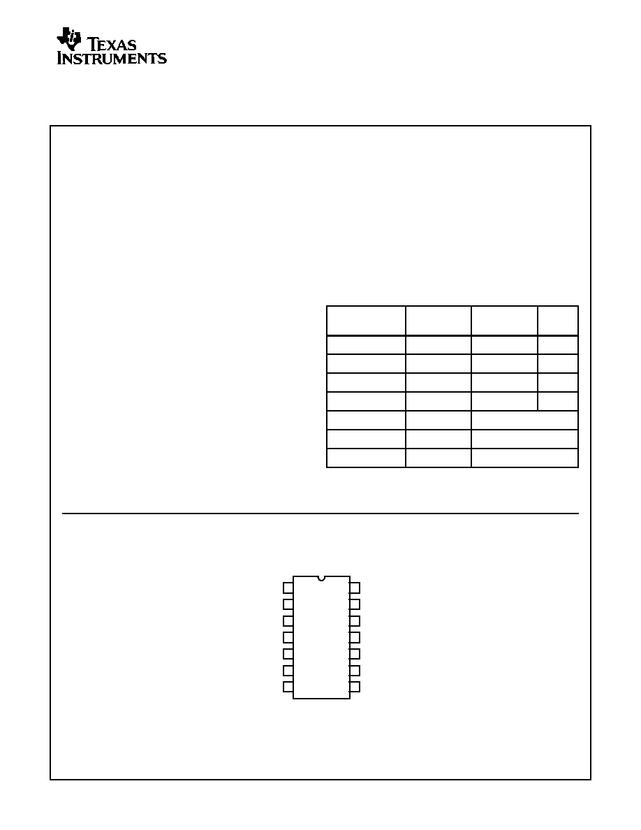
Pinout
CD74HC86, CD74HCT86
(PDIP, SOIC)
TOP VIEW
Ordering Information
PART NUMBER
TEMP. RANGE
(
o
C)
PACKAGE
PKG.
NO.
CD74HC86E
-55 to 125
14 Ld PDIP
E14.3
CD74HCT86E
-55 to 125
14 Ld PDIP
E14.3
CD74HC86M
-55 to 125
14 Ld SOIC
M14.15
CD74HCT86M
-55 to 125
14 Ld SOIC
M14.15
CD54HC86W
-55 to 125
Wafer
CD54HCT86W
-55 to 125
Wafer
CD54HC86H
-55 to 125
Die
NOTE: When ordering, use the entire part number. Add the suffix 96
to obtain the variant in the tape and reel.
1A
1B
1Y
2A
2B
2Y
GND
V
CC
4B
4A
4Y
3B
3A
3Y
1
2
3
4
5
6
7
14
13
12
11
10
9
8
August 1997
CAUTION: These devices are sensitive to electrostatic discharge. Users should follow proper IC Handling Procedures.
Copyright
©
Harris Corporation 1997
CD74HC86,
CD74HCT86
High Speed CMOS Logic
Quad 2-Input EXCLUSIVE OR Gate
File Number
1644.1
[ /Title
(CD74
HC86,
CD74
HCT86
)
/Sub-
ject
(High
Speed
CMOS
Logic
Quad
2-Input
EXCL
USIVE
OR
2
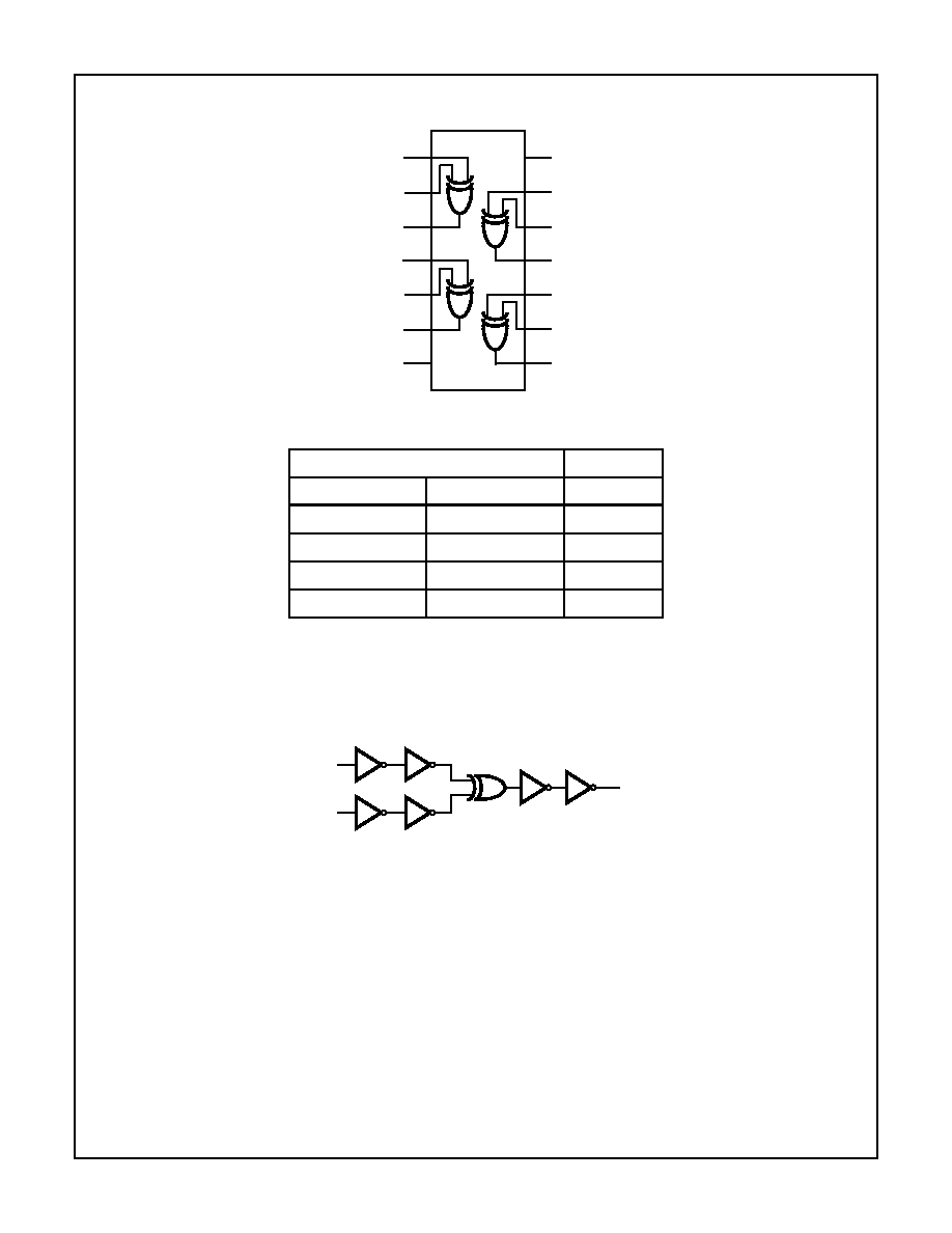
Functional Diagram
Logic Symbol
TRUTH TABLE
INPUTS
OUTPUT
nA
nB
nY
L
L
L
L
H
H
H
L
H
H
H
L
NOTE: H = High Voltage Level, L = Low Voltage Level
1A
1B
2A
2B
2Y
GND
1
2
3
4
5
6
14
13
12
11
V
CC
4Y
3Y
3B
4A
4B
10
8
7
9
3A
1Y
nA
nB
nY
CD74HC86, CD74HCT86
3
Absolute Maximum Ratings
Thermal Information
DC Supply Voltage, V
CC
. . . . . . . . . . . . . . . . . . . . . . . . -0.5V to 7V
DC Input Diode Current, I
IK
For V
I
< -0.5V or V
I
> V
CC
+ 0.5V
. . . . . . . . . . . . . . . . . . . . . .±
20mA
DC Output Diode Current, I
OK
For V
O
< -0.5V or V
O
> V
CC
+ 0.5V
. . . . . . . . . . . . . . . . . . . .±
20mA
DC Output Source or Sink Current per Output Pin, I
O
For V
O
> -0.5V or V
O
< V
CC
+ 0.5V
. . . . . . . . . . . . . . . . . . . .±
25mA
DC V
CC
or Ground Current, I
CC or
I
GND
. . . . . . . . . . . . . . . . . .±
50mA
Operating Conditions
Temperature Range (T
A
) . . . . . . . . . . . . . . . . . . . . . -55
o
C to 125
o
C
Supply Voltage Range, V
CC
HC Types . . . . . . . . . . . . . . . . . . . . . . . . . . . . . . . . . . . . .2V to 6V
HCT Types . . . . . . . . . . . . . . . . . . . . . . . . . . . . . . . . .4.5V to 5.5V
DC Input or Output Voltage, V
I
, V
O
. . . . . . . . . . . . . . . . . 0V to V
CC
Input Rise and Fall Time
2V . . . . . . . . . . . . . . . . . . . . . . . . . . . . . . . . . . . . . . 1000ns (Max)
4.5V. . . . . . . . . . . . . . . . . . . . . . . . . . . . . . . . . . . . . . 500ns (Max)
6V . . . . . . . . . . . . . . . . . . . . . . . . . . . . . . . . . . . . . . . 400ns (Max)
Thermal Resistance (Typical, Note 1)
JA
(
o
C/W)
PDIP Package . . . . . . . . . . . . . . . . . . . . . . . . . . . . .
100
SOIC Package . . . . . . . . . . . . . . . . . . . . . . . . . . . . .
180
Maximum Junction Temperature . . . . . . . . . . . . . . . . . . . . . . . 150
o
C
Maximum Storage Temperature Range . . . . . . . . . .-65
o
C to 150
o
C
Maximum Lead Temperature (Soldering 10s) . . . . . . . . . . . . . 300
o
C
(SOIC - Lead Tips Only)
CAUTION: Stresses above those listed in "Absolute Maximum Ratings" may cause permanent damage to the device. This is a stress only rating and operation
of the device at these or any other conditions above those indicated in the operational sections of this specification is not implied.
NOTE:
1.
JA
is measured with the component mounted on an evaluation PC board in free air.
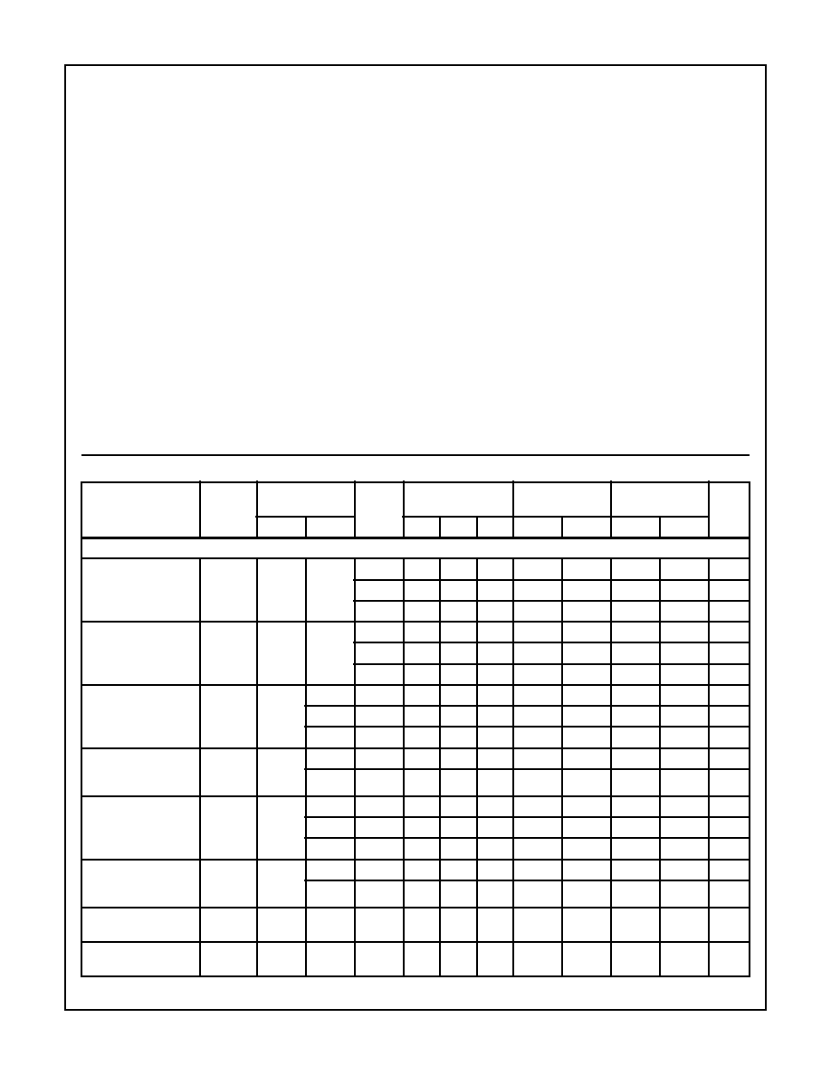
DC Electrical Specifications
PARAMETER
SYMBOL
TEST
CONDITIONS
V
CC
(V)
25
o
C
-40
o
C TO +85
o
C
-55
o
C TO 125
o
C
UNITS
V
I
(V)
I
O
(mA)
MIN
TYP
MAX
MIN
MAX
MIN
MAX
HC TYPES
High Level Input
Voltage
V
IH
-
-
2
1.5
-
-
1.5
-
1.5
-
V
4.5
3.15
-
-
3.15
-
3.15
-
V
6
4.2
-
-
4.2
-
4.2
-
V
Low Level Input
Voltage
V
IL
-
-
2
-
-
0.5
-
0.5
-
0.5
V
4.5
-
-
1.35
-
1.35
-
1.35
V
6
-
-
1.8
-
1.8
-
1.8
V
High Level Output
Voltage
CMOS Loads
V
OH
V
IH
or
V
IL
-0.02
2
1.9
-
-
1.9
-
1.9
-
V
-0.02
4.5
4.4
-
-
4.4
-
4.4
-
V
-0.02
6
5.9
-
-
5.9
-
5.9
-
V
High Level Output
Voltage
TTL Loads
-4
4.5
3.98
-
-
3.84
-
3.7
-
V
-5.2
6
5.48
-
-
5.34
-
5.2
-
V
Low Level Output
Voltage
CMOS Loads
V
OL
V
IH
or
V
IL
0.02
2
-
-
0.1
-
0.1
-
0.1
V
0.02
4.5
-
-
0.1
-
0.1
-
0.1
V
0.02
6
-
-
0.1
-
0.1
-
0.1
V
Low Level Output
Voltage
TTL Loads
4
4.5
-
-
0.26
-
0.33
-
0.4
V
5.2
6
-
-
0.26
-
0.33
-
0.4
V
Input Leakage
Current
I
I
V
CC
or
GND
-
6
-
-
±
0.1
-
±
1
-
±
1
µ
A
Quiescent Device
Current
I
CC
V
CC
or
GND
0
6
-
-
2
-
20
-
40
µ
A
CD74HC86, CD74HCT86
4
HCT TYPES
High Level Input
Voltage
V
IH
-
-
4.5 to
5.5
2
-
-
2
-
2
-
V
Low Level Input
Voltage
V
IL
-
-
4.5 to
5.5
-
-
0.8
-
0.8
-
0.8
V
High Level Output
Voltage
CMOS Loads
V
OH
V
IH
or
V
IL
-0.02
4.5
4.4
-
-
4.4
-
4.4
-
V
High Level Output
Voltage
TTL Loads
-4
4.5
3.98
-
-
3.84
-
3.7
-
V
Low Level Output
Voltage
CMOS Loads
V
OL
V
IH
or
V
IL
-0.02
4.5
-
-
0.1
-
0.1
-
0.1
V
Low Level Output
Voltage
TTL Loads
4
4.5
-
-
0.26
-
0.33
-
0.4
V
Input Leakage
Current
I
I
V
CC
and
GND
0
5.5
-
±
0.1
-
±
1
-
±
1
µ
A
Quiescent Device
Current
I
CC
V
CC
or
GND
0
5.5
-
-
2
-
20
-
40
µ
A
Additional Quiescent
Device Current Per
Input Pin: 1 Unit Load
(Note 2)
I
CC
V
CC
-2.1
-
4.5 to
5.5
-
100
360
-
450
-
490
µ
A
NOTE:
2. For dual-supply systems theorectical worst case (V
I
= 2.4V, V
CC
= 5.5V) specification is 1.8mA.
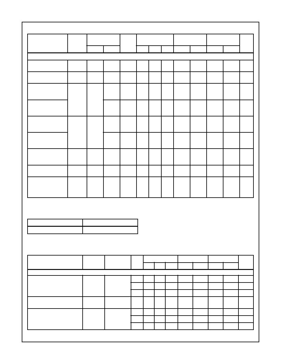
DC Electrical Specifications
(Continued)
PARAMETER
SYMBOL
TEST
CONDITIONS
V
CC
(V)
25
o
C
-40
o
C TO +85
o
C
-55
o
C TO 125
o
C
UNITS
V
I
(V)
I
O
(mA)
MIN
TYP
MAX
MIN
MAX
MIN
MAX
HCT Input Loading Table
INPUT
UNIT LOADS
All
1
NOTE: Unit Load is
I
CC
limit specified in DC Electrical
Specifications table, e.g. 360
µ
A max at 25
o
C.
Switching Specifications
Input t
r
, t
f
= 6ns
PARAMETER
SYMBOL
TEST
CONDITIONS
V
CC
(V)
25
o
C
-40
o
C TO 85
o
C
-55
o
C TO 125
o
C
UNITS
MIN
TYP
MAX
MIN
MAX
MIN
MAX
HC TYPES
Propagation Delay,Input to
Output (Figure 1)
t
PLH
, t
PHL
C
L
= 50pF
2
-
-
120
-
150
-
180
ns
4.5
-
-
24
-
30
-
36
ns
6
-
-
20
-
26
-
31
ns
Propagation Delay, Data Input to
Output Y
t
PLH
, t
PHL
C
L
= 15pF
5
-
9
-
-
-
-
-
ns
Transition Times (Figure 1)
t
TLH
, t
THL
C
L
= 50pF
2
-
-
75
-
95
-
110
ns
4.5
-
-
15
-
19
-
22
ns
6
-
-
13
-
16
-
19
ns
CD74HC86, CD74HCT86
5
Input Capacitance
C
I
-
-
-
-
10
-
10
-
10
pF
Power Dissipation Capacitance
(Notes 3, 4)
C
PD
-
5
-
22
-
-
-
-
-
pF
HCT TYPES
Propagation Delay, Input to
Output (Figure 2)
t
PLH
, t
PHL
C
L
= 50pF
4.5
-
-
32
-
40
-
48
ns
Propagation Delay, Data Input to
Output Y
t
PLH
, t
PHL
C
L
= 15pF
5
-
13
-
-
-
-
-
ns
Transition Times (Figure 2)
t
TLH
, t
THL
C
L
= 50pF
4.5
-
-
15
-
19
-
22
ns
Input Capacitance
C
I
-
-
-
-
10
-
10
-
10
pF
Power Dissipation Capacitance
(Notes 3, 4)
C
PD
-
5
-
27
-
-
-
-
-
pF
NOTES:
3. C
PD
is used to determine the dynamic power consumption, per gate.
4. P
D
= V
CC
2
f
i
(C
PD
+ C
L
) where f
i
= input frequency, C
L
= output load capacitance, V
CC
= supply voltage.
Switching Specifications
Input t
r
, t
f
= 6ns (Continued)
PARAMETER
SYMBOL
TEST
CONDITIONS
V
CC
(V)
25
o
C
-40
o
C TO 85
o
C
-55
o
C TO 125
o
C
UNITS
MIN
TYP
MAX
MIN
MAX
MIN
MAX
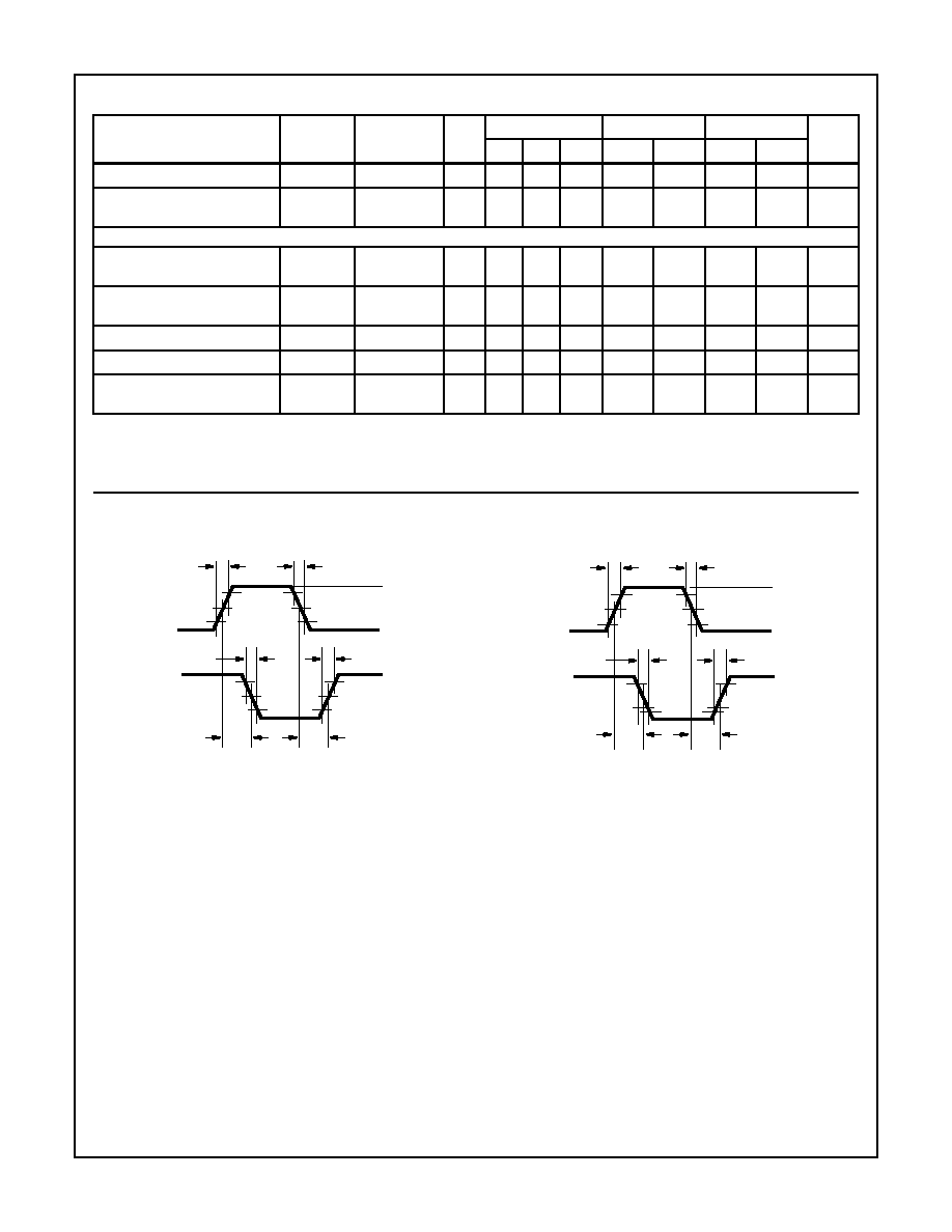
Test Circuits and Waveforms
FIGURE 1. HC AND HCU TRANSITION TIMES AND PROPAGA-
TION DELAY TIMES, COMBINATION LOGIC
FIGURE 2. HCT TRANSITION TIMES AND PROPAGATION
DELAY TIMES, COMBINATION LOGIC
t
PHL
t
PLH
t
THL
t
TLH
90%
50%
10%
50%
10%
INVERTING
OUTPUT
INPUT
GND
V
CC
t
r
= 6ns
t
f
= 6ns
90%
t
PHL
t
PLH
t
THL
t
TLH
2.7V
1.3V
0.3V
1.3V
10%
INVERTING
OUTPUT
INPUT
GND
3V
t
r
= 6ns
t
f
= 6ns
90%
CD74HC86, CD74HCT86