1
Data sheet acquired from Harris Semiconductor
SCHS153A
Features
∑ Common Select Inputs
∑ Separate Enable Inputs
∑ Buffered inputs and Outputs
∑ Fanout (Over Temperature Range)
- Standard Outputs . . . . . . . . . . . . . . . 10 LSTTL Loads
- Bus Driver Outputs . . . . . . . . . . . . . 15 LSTTL Loads
∑ Wide Operating Temperature Range . . . -55
o
C to 125
o
C
∑ Balanced Propagation Delay and Transition Times
∑ Significant Power Reduction Compared to LSTTL
Logic ICs
∑ HC Types
- 2V to 6V Operation
- High Noise Immunity: N
IL
= 30%, N
IH
= 30%of V
CC
at
V
CC
= 5V
∑ HCT Types
- 4.5V to 5.5V Operation
- Direct LSTTL Input Logic Compatibility,
V
IL
= 0.8V (Max), V
IH
= 2V (Min)
- CMOS Input Compatibility, I
l
1
µ
A at V
OL
, V
OH
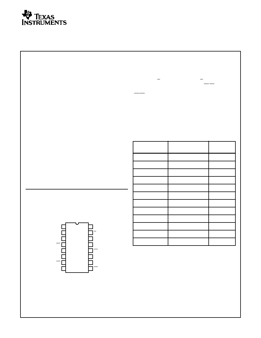
Pinout
CD54HC157, CD54HCT157, CD54HC158, CD54HCT158
(CERDIP)
CD74HC157, CD74HCT157, CD74HC158, CD74HCT158
(PDIP, SOIC)
TOP VIEW
Description
The 'HC157, 'HCT157, 'HC158, and 'HCT158 are quad 2-
input multiplexers which select four bits of data from two
sources under the control of a common Select input (S). The
Enable input (E) is active Low. When (E) is High, all of the
outputs in the 158, the inverting type, (1Y-4Y) are forced
High and in the 157, the non-inverting type, all of the outputs
(1Y-4Y) are forced Low, regardless of all other input
conditions.
Moving data from two groups of registers to four common
output busses is a common use of these devices. The state
of the Select input determines the particular register from
which the data comes. They can also be used as function
generators.
14
15
16
9
13
12
11
10
1
2
3
4
5
7
6
8
S
1I
0
1I
1
1Y
2I
0
2I
1
GND
2Y
V
CC
4I
0
4I
1
4Y
3I
0
3I
1
3Y
E
Ordering Information
PART NUMBER
TEMP. RANGE
(
o
C)
PACKAGE
CD54HC157F
-55 to 125
16 Ld CERDIP
CD54HC157F3A
-55 to 125
16 Ld CERDIP
CD74HC157E
-55 to 125
16 Ld PDIP
CD74HC157M
-55 to 125
16 Ld SOIC
CD54HCT157F3A
-55 to 125
16 Ld CERDIP
CD74HCT157E
-55 to 125
16 Ld PDIP
CD74HCT157M
-55 to 125
16 Ld SOIC
CD54HC158F3A
-55 to 125
16 Ld CERDIP
CD74HC158E
-55 to 125
16 Ld PDIP
CD74HC158M
-55 to 125
16 Ld SOIC
CD54HCT158F3A
-55 to 125
16 Ld CERDIP
CD74HCT158E
-55 to 125
16 Ld PDIP
NOTES:
1. When ordering, use the entire part number. Add the suffix 96 to
obtain the variant in the tape and reel.
2. Wafer or die for this part number is available which meets all elec-
trical specifications. Please contact your local TI sales office or
customer service for ordering information.
September 1997 - Revised May 2000
CAUTION: These devices are sensitive to electrostatic discharge. Users should follow proper IC Handling Procedures.
Copyright
©
2000, Texas Instruments Incorporated
CD54/74HC157, CD54/74HCT157,
CD54/74HC158, CD54/74HCT158
High Speed CMOS Logic
Quad 2-Input Multiplexers
[ /Title
(CD74H
C157,
CD74H
CT157,
CD74H
C158,
CD74H
CT158)
/Subject
(High
Speed
2
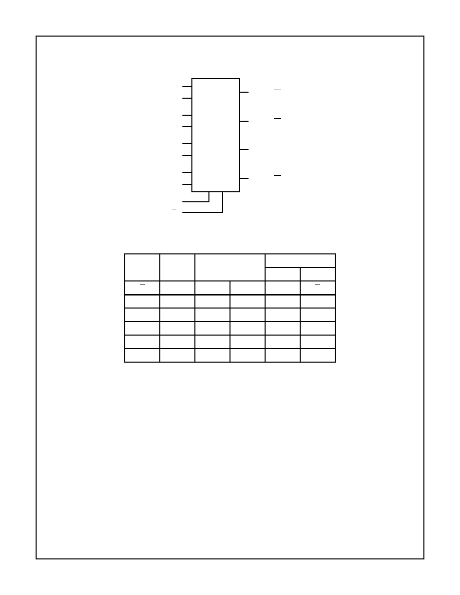
Functional Diagram
TRUTH TABLE
ENABLE
SELECT
INPUT
DATA INPUTS
OUTPUT
157
158
E
S
I0
I1
Y
Y
H
X
X
X
L
H
L
L
L
X
L
H
L
L
H
X
H
L
L
H
X
L
L
H
L
H
X
H
H
L
NOTE: H = High Voltage Level, L = Low Voltage Level, X = Don't Care
2
3
5
6
10
13
14
11
4
7
12
9
4Y
3Y
2Y
1Y
1Y
4Y
3Y
2Y
HC/HCT
157
HC/HCT
158
1I
0
1I
1
2I
0
2I
1
3I
0
3I
1
4I
0
4I
1
S
E
1
15
CD54/74HC157, CD54/74HCT157, CD54/74HC158, CD54/74HCT158
3
Absolute Maximum Ratings
Thermal Information
DC Supply Voltage, V
CC
. . . . . . . . . . . . . . . . . . . . . . . . -0.5V to 7V
DC Input Diode Current, I
IK
For V
I
< -0.5V or V
I
> V
CC
+ 0.5V
. . . . . . . . . . . . . . . . . . . . . .±
20mA
DC Output Diode Current, I
OK
For V
O
< -0.5V or V
O
> V
CC
+ 0.5V
. . . . . . . . . . . . . . . . . . . .±
20mA
DC Output Source or Sink Current per Output Pin, I
O
For V
O
> -0.5V or V
O
< V
CC
+ 0.5V
. . . . . . . . . . . . . . . . . . . .±
25mA
DC V
CC
or Ground Current, I
CC or
I
GND
. . . . . . . . . . . . . . . . . .±
50mA
Operating Conditions
Temperature Range (T
A
) . . . . . . . . . . . . . . . . . . . . . -55
o
C to 125
o
C
Supply Voltage Range, V
CC
HC Types . . . . . . . . . . . . . . . . . . . . . . . . . . . . . . . . . . . . .2V to 6V
HCT Types . . . . . . . . . . . . . . . . . . . . . . . . . . . . . . . . .4.5V to 5.5V
DC Input or Output Voltage, V
I
, V
O
. . . . . . . . . . . . . . . . . 0V to V
CC
Input Rise and Fall Time
2V . . . . . . . . . . . . . . . . . . . . . . . . . . . . . . . . . . . . . . 1000ns (Max)
4.5V. . . . . . . . . . . . . . . . . . . . . . . . . . . . . . . . . . . . . . 500ns (Max)
6V . . . . . . . . . . . . . . . . . . . . . . . . . . . . . . . . . . . . . . . 400ns (Max)
Thermal Resistance (Typical, Note 3)
JA
(
o
C/W)
PDIP Package . . . . . . . . . . . . . . . . . . . . . . . . . . . . .
90
SOIC Package . . . . . . . . . . . . . . . . . . . . . . . . . . . . .
115
Maximum Junction Temperature . . . . . . . . . . . . . . . . . . . . . . . 150
o
C
Maximum Storage Temperature Range . . . . . . . . . .-65
o
C to 150
o
C
Maximum Lead Temperature (Soldering 10s) . . . . . . . . . . . . . 300
o
C
(SOIC - Lead Tips Only)
CAUTION: Stresses above those listed in "Absolute Maximum Ratings" may cause permanent damage to the device. This is a stress only rating and operation
of the device at these or any other conditions above those indicated in the operational sections of this specification is not implied.
NOTE:
3.
JA
is measured with the component mounted on an evaluation PC board in free air.
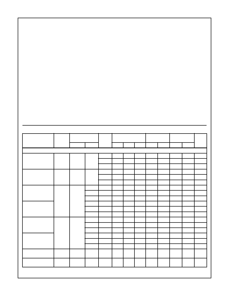
DC Electrical Specifications
PARAMETER
SYMBOL
TEST
CONDITIONS
V
CC
(V)
25
o
C
-40
o
C TO 85
o
C -55
o
C TO 125
o
C
UNITS
V
I
(V)
I
O
(mA)
MIN
TYP
MAX
MIN
MAX
MIN
MAX
HC TYPES
High Level Input
Voltage
V
IH
-
-
2
1.5
-
-
1.5
-
1.5
-
V
4.5
3.15
-
-
3.15
-
3.15
-
V
6
4.2
-
-
4.2
-
4.2
-
V
Low Level Input
Voltage
V
IL
-
-
2
-
-
0.5
-
0.5
-
0.5
V
4.5
-
-
1.35
-
1.35
-
1.35
V
6
-
-
1.8
-
1.8
-
1.8
V
High Level Output
Voltage
CMOS Loads
V
OH
V
IH
or V
IL
-0.02
2
1.9
-
-
1.9
-
1.9
-
V
-0.02
4.5
4.4
-
-
4.4
-
4.4
-
V
-0.02
6
5.9
-
-
5.9
-
5.9
-
V
High Level Output
Voltage
TTL Loads
-
-
-
-
-
-
-
-
-
V
-4
4.5
3.98
-
-
3.84
-
3.7
-
V
-5.2
6
5.48
-
-
5.34
-
5.2
-
V
Low Level Output
Voltage
CMOS Loads
V
OL
V
IH
or V
IL
0.02
2
-
-
0.1
-
0.1
-
0.1
V
0.02
4.5
-
-
0.1
-
0.1
-
0.1
V
0.02
6
-
-
0.1
-
0.1
-
0.1
V
Low Level Output
Voltage
TTL Loads
-
-
-
-
-
-
-
-
-
V
4
4.5
-
-
0.26
-
0.33
-
0.4
V
5.2
6
-
-
0.26
-
0.33
-
0.4
V
Input Leakage
Current
I
I
V
CC
or
GND
-
6
-
-
±
0.1
-
±
1
-
±
1
µ
A
Quiescent Device
Current
I
CC
V
CC
or
GND
0
6
-
-
8
-
80
-
160
µ
A
CD54/74HC157, CD54/74HCT157, CD54/74HC158, CD54/74HCT158
4
HCT TYPES
High Level Input
Voltage
V
IH
-
-
4.5 to
5.5
2
-
-
2
-
2
-
V
Low Level Input
Voltage
V
IL
-
-
4.5 to
5.5
-
-
0.8
-
0.8
-
0.8
V
High Level Output
Voltage
CMOS Loads
V
OH
V
IH
or V
IL
-0.02
4.5
4.4
-
-
4.4
-
4.4
-
V
High Level Output
Voltage
TTL Loads
-4
4.5
3.98
-
-
3.84
-
3.7
-
V
Low Level Output
Voltage
CMOS Loads
V
OL
V
IH
or V
IL
0.02
4.5
-
-
0.1
-
0.1
-
0.1
V
Low Level Output
Voltage
TTL Loads
4
4.5
-
-
0.26
-
0.33
-
0.4
V
Input Leakage
Current
I
I
V
CC
and
GND
0
5.5
-
±
0.1
-
±
1
-
±
1
µ
A
Quiescent Device
Current
I
CC
V
CC
or
GND
0
5.5
-
-
8
-
80
-
160
µ
A
Additional Quiescent
Device Current Per
Input Pin: 1 Unit Load
I
CC
V
CC
-2.1
-
4.5 to
5.5
-
100
360
-
450
-
490
µ
A
NOTE: For dual-supply systems theoretical worst case (V
I
= 2.4V, V
CC
= 5.5V) specification is 1.8mA.
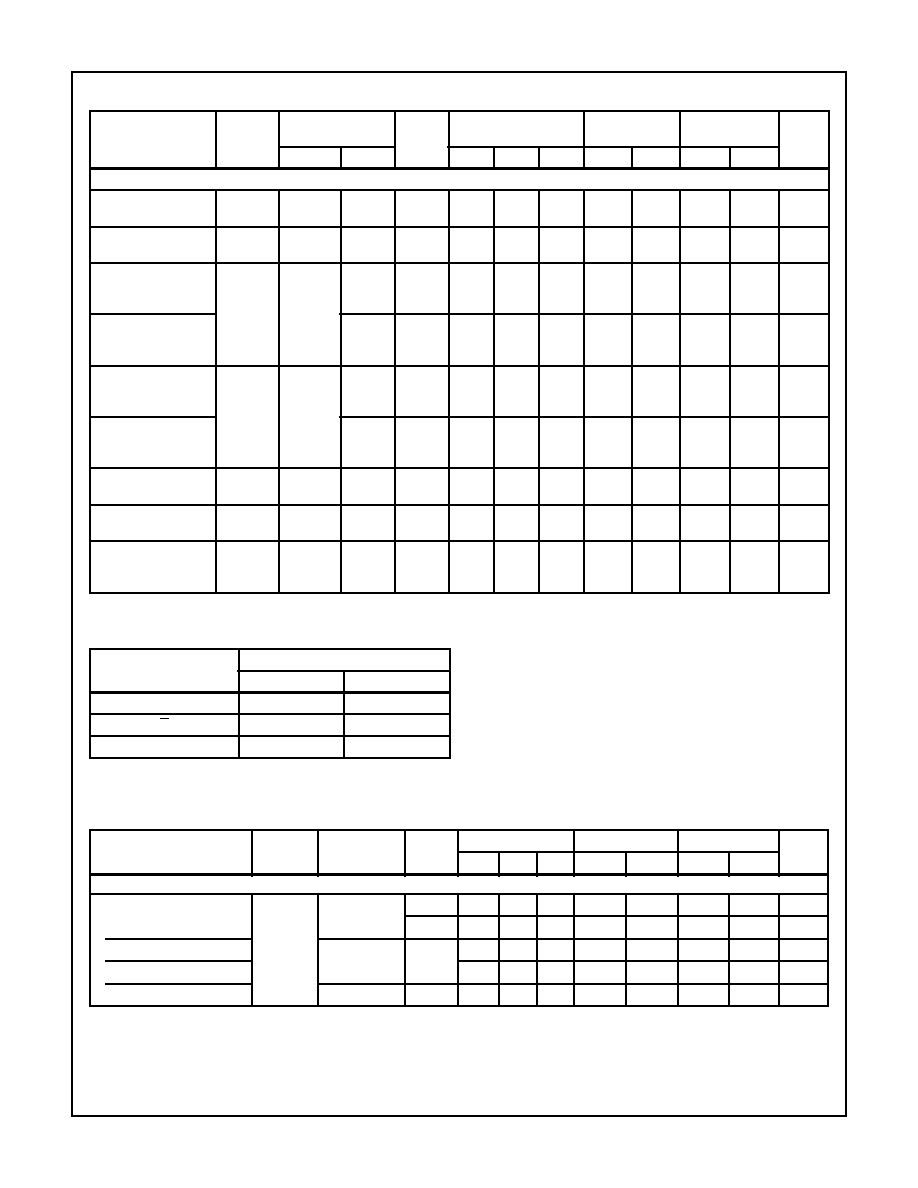
DC Electrical Specifications
(Continued)
PARAMETER
SYMBOL
TEST
CONDITIONS
V
CC
(V)
25
o
C
-40
o
C TO 85
o
C -55
o
C TO 125
o
C
UNITS
V
I
(V)
I
O
(mA)
MIN
TYP
MAX
MIN
MAX
MIN
MAX
HCT Input Loading Table
INPUT
UNIT LOADS
HCT157
HCT158
I (All)
0.95
0.4
E
0.6
0.6
S
3
2.8
NOTE: Unit Load is
I
CC
limit specified in DC Electrical Table, e.g.,
360
µ
A max at 25
o
C.
Switching Specifications
Input t
r
, t
f
= 6ns
PARAMETER
SYMBOL
TEST
CONDITIONS
V
CC
(V)
25
o
C
-40
o
C TO 85
o
C
-55
o
C TO 125
o
C
UNITS
MIN
TYP
MAX
MIN
MAX
MIN
MAX
HC/HCT157 TYPES
Propagation Delay (Figure 1) t
PLH,
t
PHL
C
L
= 50pF
2
-
-
125
-
155
-
190
ns
Data to Output
4.5
-
-
25
-
31
-
38
ns
HC157
C
L
=15pF
5
-
10
-
-
-
-
-
ns
HCT157
-
12
-
-
-
-
-
ns
C
L
= 50pF
6
-
-
21
-
26
-
32
ns
CD54/74HC157, CD54/74HCT157, CD54/74HC158, CD54/74HCT158

5
Enable to Output
t
PLH,
t
PHL
C
L
= 50pF
2
-
-
135
-
170
-
205
ns
4.5
-
-
27
-
34
-
41
ns
HC157
C
L
=15pF
5
-
11
-
-
-
-
-
ns
HCT157
-
12
-
-
-
-
-
ns
C
L
= 50pF
6
-
-
23
-
29
-
35
ns
Select to Output
t
PLH,
t
PHL
C
L
= 50pF
2
-
-
145
-
180
-
220
ns
4.5
-
-
29
-
36
-
44
ns
HC157
C
L
=15pF
5
-
12
-
-
-
-
-
ns
HCT157
-
15
-
-
-
-
-
ns
C
L
= 50pF
6
-
-
25
-
31
-
38
ns
Power Dissipation
Capacitance (Notes 4, 5)
C
PD
-
5
HC157
-
62
-
-
-
-
-
pF
HCT157
-
70
-
-
-
-
-
pF
HC/HCT158 TYPES
Data to Output
t
PLH,
t
PHL
C
L
= 50pF
2
-
-
140
-
175
-
210
ns
4.5
-
-
28
-
35
-
42
HC158
C
L
=15pF
5
-
11
-
-
-
-
-
ns
HCT 158
-
13
-
-
-
-
-
ns
C
L
= 50pF
6
-
-
24
-
30
-
36
ns
Enable to Output
t
PLH,
t
PHL
C
L
= 50pF
2
-
-
160
-
200
-
240
ns
4.5
-
-
32
-
40
-
48
ns
HC158
C
L
=15pF
5
-
13
-
-
-
-
-
ns
HCT 158
-
15
-
-
-
-
-
ns
C
L
= 50pF
6
-
-
27
-
34
-
41
ns
Select to Output
t
PLH,
t
PHL
C
L
= 50pF
2
-
-
150
-
190
-
225
ns
4.5
-
-
30
-
38
-
45
ns
HC158
C
L
=15pF
5
-
12
-
-
-
-
-
ns
HCT 158
-
14
-
-
-
-
-
ns
C
L
= 50pF
6
-
-
26
-
33
-
38
ns
Output Transition Time
t
TLH,
t
THL
C
L
= 50pF
2
-
-
75
-
95
-
110
ns
4.5
-
-
15
-
19
-
22
ns
6
-
-
13
-
16
-
19
ns
Power Dissipation
Capacitance (Notes 4, 5)
C
PD
-
5
HC158
-
35
-
-
-
-
-
pF
HCT 158
-
35
-
-
-
-
-
pF
Input Capacitance
C
IN
C
L
= 50pF
-
-
-
10
-
10
-
10
pF
NOTES:
4. C
PD
is used to determine the dynamic power consumption, per multiplexer.
5. P
D
= V
CC
2
f
i
(C
PD
+ C
L
) where f
i
= input frequency, C
L
= output load capacitance, V
CC
= supply voltage.
Switching Specifications
Input t
r
, t
f
= 6ns (Continued)
PARAMETER
SYMBOL
TEST
CONDITIONS
V
CC
(V)
25
o
C
-40
o
C TO 85
o
C
-55
o
C TO 125
o
C
UNITS
MIN
TYP
MAX
MIN
MAX
MIN
MAX
CD54/74HC157, CD54/74HCT157, CD54/74HC158, CD54/74HCT158