1
Data sheet acquired from Harris Semiconductor
SCHS155A
Features
∑ Buffered Inputs
∑ Asynchronous Master Reset
∑ Typical f
MAX
= 50MHz at V
CC
= 5V, C
L
= 15pF,
T
A
= 25
o
C
∑ Fanout (Over Temperature Range)
- Standard Outputs . . . . . . . . . . . . . . . 10 LSTTL Loads
- Bus Driver Outputs . . . . . . . . . . . . . 15 LSTTL Loads
∑ Wide Operating Temperature Range . . . -55
o
C to 125
o
C
∑ Balanced Propagation Delay and Transition Times
∑ Significant Power Reduction Compared to LSTTL
Logic ICs
∑ HC Types
- 2V to 6V Operation
- High Noise Immunity: N
IL
= 30%, N
IH
= 30% of V
CC
at V
CC
= 5V
∑ HCT Types
- 4.5V to 5.5V Operation
- Direct LSTTL Input Logic Compatibility,
V
IL
= 0.8V (Max), V
IH
= 2V (Min)
- CMOS Input Compatibility, I
l
1
µ
A at V
OL
, V
OH
Description
The 'HC164 and 'HCT164 are 8-bit serial-in parallel-out shift
registers with asynchronous reset. Data is shifted on the
positive edge of Clock (CP). A LOW on the Master Reset
(MR) pin resets the shift register and all outputs go to the
LOW state regardless of the input conditions. Two Serial
Data inputs (DS1 and DS2) are provided, either one can be
used as a Data Enable control.
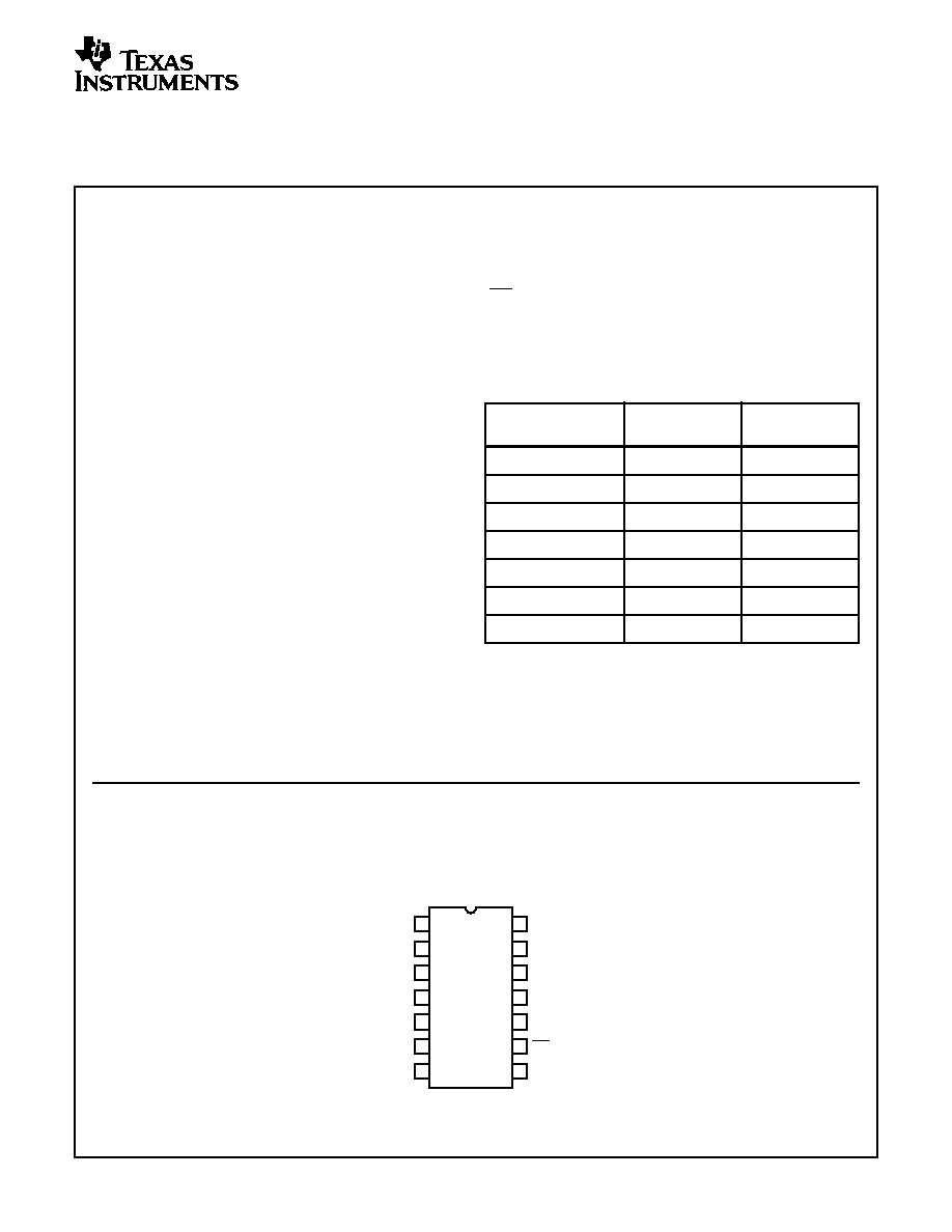
Pinout
CD54HC164, CD54HCT164
(CERDIP)
CD74HC164, CD74HCT164
(PDIP, SOIC)
TOP VIEW
Ordering Information
PART NUMBER
TEMP. RANGE
(
o
C)
PACKAGE
CD54HC164F
-55 to 125
14 Ld CERDIP
CD54HC164F3A
-55 to 125
14 Ld CERDIP
CD74HC164E
-55 to 125
14 Ld PDIP
CD74HC164M
-55 to 125
14 Ld SOIC
CD54HCT164F3A
-55 to 125
14 Ld CERDIP
CD74HCT164E
-55 to 125
14 Ld PDIP
CD74HCT164M
-55 to 125
14 Ld SOIC
NOTE:
1. When ordering, use the entire part number. Add the suffix 96 to
obtain the variant in the tape and reel.
2. Wafer and die is available which meets all electrical
specifications. Please contact your local TI sales office or
customer service for ordering information.
DS1
DS2
Q
0
Q
1
Q
2
Q
3
GND
V
CC
Q
7
Q
6
Q
5
Q
4
MR
CP
1
2
3
4
5
6
7
14
13
12
11
10
9
8
October 1997 - Revised May 2000
CAUTION: These devices are sensitive to electrostatic discharge. Users should follow proper IC Handling Procedures.
Copyright
©
2000, Texas Instruments Incorporated
CD54/74HC164,
CD54/74HCT164
High Speed CMOS Logic
8-Bit Serial-In/Parallel-Out Shift Register
[ /Title
(CD74
HC164
,
CD74
HCT16
4)
/Sub-
ject
(High
Speed
CMOS
Logic
8-Bit
Serial-
In/Par-
allel-
2
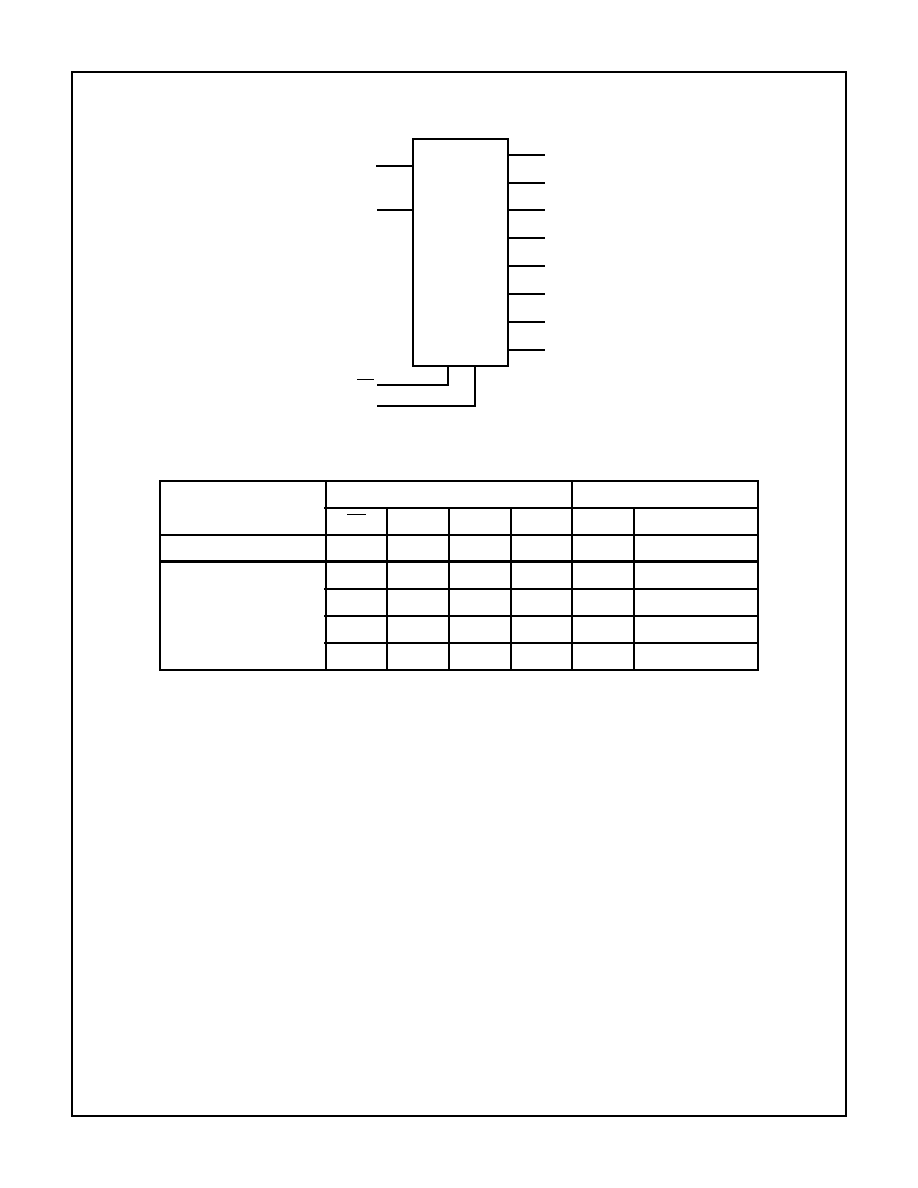
Functional Diagram
TRUTH TABLE
OPERATING MODE
INPUTS
OUTPUTS
MR
CP
DS1
DS2
Q
0
Q
1
- Q
7
RESET (CLEAR)
L
X
X
X
L
L - L
Shift
H
l
l
L
q
0 -
q
6
H
l
h
L
q
0 -
q
6
H
h
l
L
q
0 -
q
6
H
h
h
H
q
0 -
q
6
NOTES:
H = High Voltage Level.
h = High Voltage Level One Set-up Time Prior To The Low-to-high Clock Transition.
l = Low Voltage Level One Set-up Time Prior To The Low-to-high Clock Transition.
L = Low Voltage Level.
X = Don't Care.
= Transition from Low to High Level.
q
n
= Lower Case Letters Indicate The State Of the Reference Input Clock Transition.
3
4
5
6
11
13
12
10
1
DS1
Q
0
Q
1
Q
2
Q
3
Q
4
Q
5
Q
6
Q
7
CP
MR
9
8
2
DS2
GND = 7
V
CC
= 14
CD54/74HC164, CD54/74HCT164
3
Absolute Maximum Ratings
Thermal Information
DC Supply Voltage, V
CC
. . . . . . . . . . . . . . . . . . . . . . . . -0.5V to 7V
DC Input Diode Current, I
IK
For V
I
< -0.5V or V
I
> V
CC
+ 0.5V
. . . . . . . . . . . . . . . . . . . . . .±
20mA
DC Output Diode Current, I
OK
For V
O
< -0.5V or V
O
> V
CC
+ 0.5V
. . . . . . . . . . . . . . . . . . . .±
20mA
DC Output Source or Sink Current per Output Pin, I
O
For V
O
> -0.5V or V
O
< V
CC
+ 0.5V
. . . . . . . . . . . . . . . . . . . .±
25mA
DC V
CC
or Ground Current, I
CC or
I
GND
. . . . . . . . . . . . . . . . . .±
50mA
Operating Conditions
Temperature Range (T
A
) . . . . . . . . . . . . . . . . . . . . . -55
o
C to 125
o
C
Supply Voltage Range, V
CC
HC Types . . . . . . . . . . . . . . . . . . . . . . . . . . . . . . . . . . . . .2V to 6V
HCT Types . . . . . . . . . . . . . . . . . . . . . . . . . . . . . . . . .4.5V to 5.5V
DC Input or Output Voltage, V
I
, V
O
. . . . . . . . . . . . . . . . . 0V to V
CC
Input Rise and Fall Time
2V . . . . . . . . . . . . . . . . . . . . . . . . . . . . . . . . . . . . . . 1000ns (Max)
4.5V. . . . . . . . . . . . . . . . . . . . . . . . . . . . . . . . . . . . . . 500ns (Max)
6V . . . . . . . . . . . . . . . . . . . . . . . . . . . . . . . . . . . . . . . 400ns (Max)
Thermal Resistance (Typical, Note 3)
JA
(
o
C/W)
PDIP Package . . . . . . . . . . . . . . . . . . . . . . . . . . . . .
90
SOIC Package . . . . . . . . . . . . . . . . . . . . . . . . . . . . .
175
Maximum Junction Temperature . . . . . . . . . . . . . . . . . . . . . . . 150
o
C
Maximum Storage Temperature Range . . . . . . . . . .-65
o
C to 150
o
C
Maximum Lead Temperature (Soldering 10s) . . . . . . . . . . . . . 300
o
C
(SOIC - Lead Tips Only)
CAUTION: Stresses above those listed in "Absolute Maximum Ratings" may cause permanent damage to the device. This is a stress only rating and operation
of the device at these or any other conditions above those indicated in the operational sections of this specification is not implied.
NOTE:
3.
JA
is measured with the component mounted on an evaluation PC board in free air.
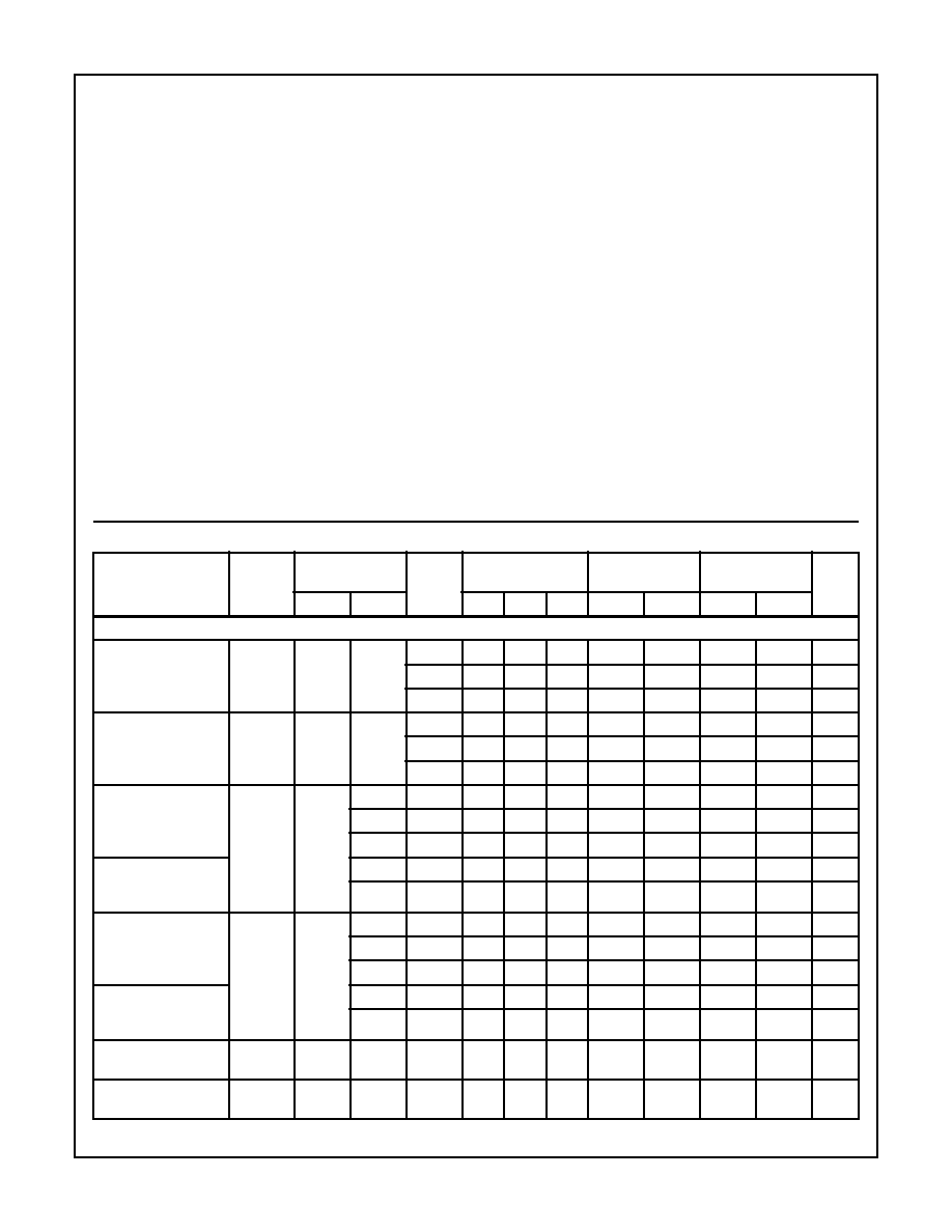
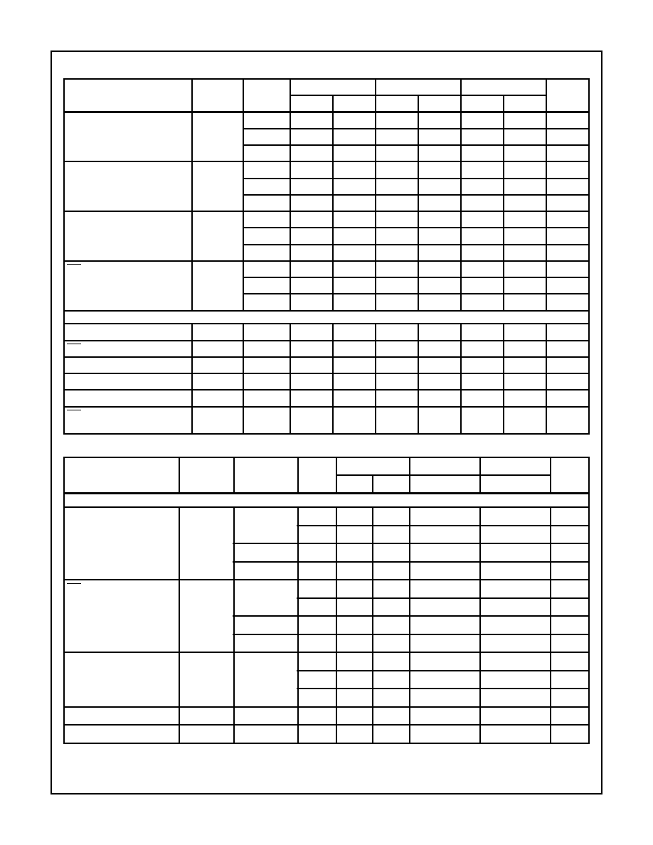
DC Electrical Specifications
PARAMETER
SYMBOL
TEST
CONDITIONS
V
CC
(V)
25
o
C
-40
o
C TO 85
o
C
-55
o
C TO 125
o
C
UNITS
V
I
(V)
I
O
(mA)
MIN
TYP
MAX
MIN
MAX
MIN
MAX
HC TYPES
High Level Input
Voltage
V
IH
-
-
2
1.5
-
-
1.5
-
1.5
-
V
4.5
3.15
-
-
3.15
-
3.15
-
V
6
4.2
-
-
4.2
-
4.2
-
V
Low Level Input
Voltage
V
IL
-
-
2
-
-
0.5
-
0.5
-
0.5
V
4.5
-
-
1.35
-
1.35
-
1.35
V
6
-
-
1.8
-
1.8
-
1.8
V
High Level Output
Voltage
CMOS Loads
V
OH
V
IH
or
V
IL
-0.02
2
1.9
-
-
1.9
-
1.9
-
V
-0.02
4.5
4.4
-
-
4.4
-
4.4
-
V
-0.02
6
5.9
-
-
5.9
-
5.9
-
V
High Level Output
Voltage
TTL Loads
-4
4.5
3.98
-
-
3.84
-
3.7
-
V
-5.2
6
5.48
-
-
5.34
-
5.2
-
V
Low Level Output
Voltage
CMOS Loads
V
OL
V
IH
or
V
IL
0.02
2
-
-
0.1
-
0.1
-
0.1
V
0.02
4.5
-
-
0.1
-
0.1
-
0.1
V
0.02
6
-
-
0.1
-
0.1
-
0.1
V
Low Level Output
Voltage
TTL Loads
4
4.5
-
-
0.26
-
0.33
-
0.4
V
5.2
6
-
-
0.26
-
0.33
-
0.4
V
Input Leakage
Current
I
I
V
CC
or
GND
-
6
-
-
±
0.1
-
±
1
-
±
1
µ
A
Quiescent Device
Current
I
CC
V
CC
or
GND
0
6
-
-
8
-
80
-
160
µ
A
CD54/74HC164, CD54/74HCT164
4
HCT TYPES
High Level Input
Voltage
V
IH
-
-
4.5 to
5.5
2
-
-
2
-
2
-
V
Low Level Input
Voltage
V
IL
-
-
4.5 to
5.5
-
-
0.8
-
0.8
-
0.8
V
High Level Output
Voltage
CMOS Loads
V
OH
V
IH
or
V
IL
-0.02
4.5
4.4
-
-
4.4
-
4.4
-
V
High Level Output
Voltage
TTL Loads
-4
4.5
3.98
-
-
3.84
-
3.7
-
V
Low Level Output
Voltage
CMOS Loads
V
OL
V
IH
or
V
IL
0.02
4.5
-
-
0.1
-
0.1
-
0.1
V
Low Level Output
Voltage
TTL Loads
4
4.5
-
-
0.26
-
0.33
-
0.4
V
Input Leakage
Current
I
I
V
CC
to
GND
0
5.5
-
-
±
0.1
-
±
1
-
±
1
µ
A
Quiescent Device
Current
I
CC
V
CC
or
GND
0
5.5
-
-
8
-
80
-
160
µ
A
Additional Quiescent
Device Current Per
Input Pin: 1 Unit Load
(Note 4)
I
CC
V
CC
-2.1
-
4.5 to
5.5
-
100
360
-
450
-
490
µ
A
NOTE:
4. For dual-supply systems theoretical worst case (V
I
= 2.4V, V
CC
= 5.5V) specification is 1.8mA.
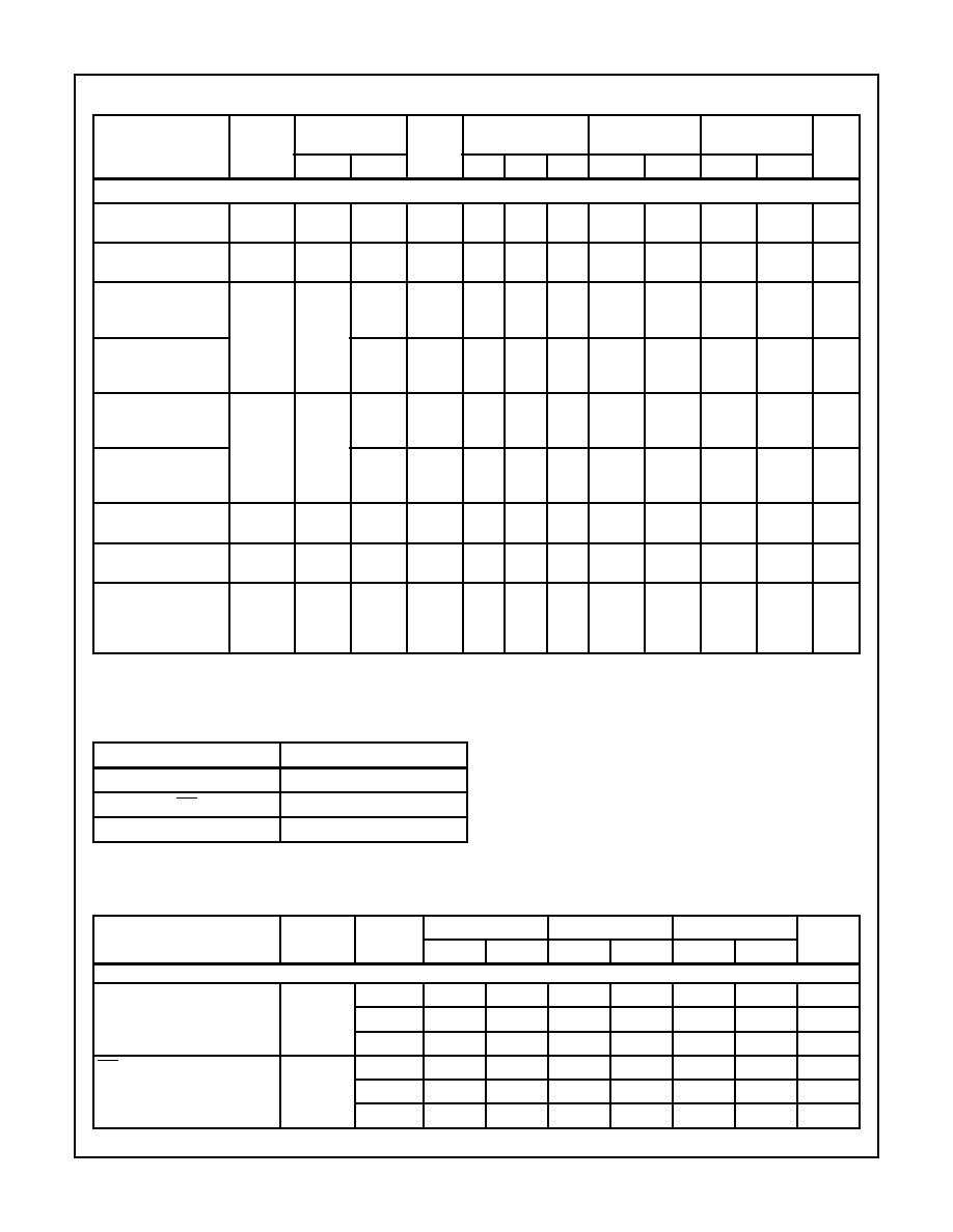
DC Electrical Specifications
(Continued)
PARAMETER
SYMBOL
TEST
CONDITIONS
V
CC
(V)
25
o
C
-40
o
C TO 85
o
C
-55
o
C TO 125
o
C
UNITS
V
I
(V)
I
O
(mA)
MIN
TYP
MAX
MIN
MAX
MIN
MAX
HCT Input Loading Table
INPUT
UNIT LOADS
Date Shift-In (1, 2)
0.3
MR
0.9
Clock
0.7
NOTE: Unit Load is
I
CC
limit specified in DC Electrical
Specifications table, e.g. 360
µ
A max at 25
o
C.
Prerequisite For Switching Function
PARAMETER
SYMBOL
V
CC
(V)
25
o
C
-40
o
C TO 85
o
C
-55
o
C TO 125
o
C
UNITS
MIN
MAX
MIN
MAX
MIN
MAX
HC TYPES
Maximum Clock Frequency
f
MAX
2
6
-
5
-
4
-
MHz
4.5
30
-
24
-
20
-
MHz
6
35
-
28
-
24
-
MHz
MR Pulse Width
t
w
2
60
-
75
-
90
-
ns
4.5
12
-
15
-
18
-
ns
6
10
-
13
-
15
-
ns
CD54/74HC164, CD54/74HCT164
5
CP Pulse Width
t
W
2
80
-
100
-
120
-
ns
4.5
16
-
20
-
24
-
ns
6
14
-
17
-
20
-
ns
Set-up Time
t
SU
2
60
-
75
-
90
-
ns
4.5
12
-
15
-
18
-
ns
6
10
-
13
-
15
-
ns
Hold Time
t
H
2
4
-
4
-
4
-
ns
4.5
4
-
4
-
4
-
ns
6
4
-
4
-
4
-
ns
MR to Clock,
Removal Time
t
REM
2
80
-
100
-
120
-
ns
4.5
16
-
20
-
24
-
ns
6
14
-
17
-
20
-
ns
HCT TYPES
Maximum Clock Frequency
f
MAX
4.5
27
-
22
-
18
-
MHz
MR Pulse Width
t
w
6
18
-
23
-
27
-
ns
CP Pulse Width
t
w
4.5
18
-
23
-
27
-
ns
Set-up Time
t
SU
6
12
-
15
-
18
-
ns
Hold Time
t
H
4.5
4
-
4
-
4
-
ns
MR to Clock,
Removal Time
t
REM
6
16
-
20
-
24
-
ns
Switching Specifications
Input t
r
, t
f
= 6ns
PARAMETER
SYMBOL
TEST
CONDITIONS
V
CC
(V)
25
o
C
-40
o
C TO 85
o
C
-55
o
C TO 125
o
C
UNITS
TYP
MAX
MAX
MAX
HC TYPES
Propagation Delay,
CP to Q
n
t
PLH
, t
PHL
C
L
= 50pF
2
-
170
212
255
ns
4.5
-
34
43
51
ns
C
L
= 15pF
5
14
-
-
-
ns
C
L
= 50pF
6
-
29
36
43
ns
MR to Q
n
t
PLH
, t
PHL
C
L
= 50pF
2
-
140
175
210
ns
4.5
-
28
35
42
ns
C
L
= 15pF
5
11
-
-
-
ns
C
L
= 50pF
6
-
24
30
36
ns
Output Transition Times
t
TLH
, t
THL
C
L
= 50pF
2
-
75
-
110
ns
4.5
-
15
-
22
ns
6
-
13
-
19
ns
Maximum Clock Frequency
f
MAX
C
L
= 15pF
5
60
-
-
-
MHz
Input Capacitance
C
IN
-
-
-
10
10
10
pF
Prerequisite For Switching Function
(Continued)
PARAMETER
SYMBOL
V
CC
(V)
25
o
C
-40
o
C TO 85
o
C
-55
o
C TO 125
o
C
UNITS
MIN
MAX
MIN
MAX
MIN
MAX
CD54/74HC164, CD54/74HCT164