1
Data sheet acquired from Harris Semiconductor
SCHS247A
Features
∑ Buffered Inputs
∑ Typical Propagation Delay
- 6.3ns at V
CC
= 5V, T
A
= 25
o
C, C
L
= 50pF
∑ Exceeds 2kV ESD Protection MIL-STD-883, Method
3015
∑ SCR-Latchup-Resistant CMOS Process and Circuit
Design
∑ Speed of Bipolar FASTTM/AS/S with Significantly
Reduced Power Consumption
∑ Balanced Propagation Delays
∑ AC Types Feature 1.5V to 5.5V Operation and
Balanced Noise Immunity at 30% of the Supply
∑
±
24mA Output Drive Current
- Fanout to 15 FASTTM ICs
- Drives 50
Transmission Lines
Description
The CD74AC253 and 'ACT253 dual 4-input multiplexers that
utilize Advanced CMOS Logic technology. One of the four
sources for each section is selected by the common Select
inputs, S0 and S1. When the Output Enable (1OE or 2OE) is
HIGH, the output is in the high-impedance state.
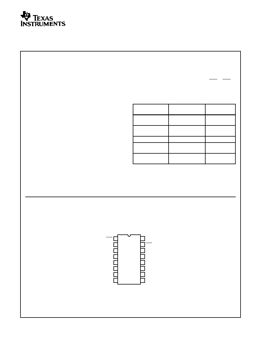
Pinout
CD54ACT253
(CERDIP)
CD74AC253, CD74ACT253
(PDIP, SOIC)
TOP VIEW
Ordering Information
PART
NUMBER
TEMP.
RANGE (
o
C)
PACKAGE
CD74AC253E
0 to 70
o
C, -40 to 85,
-55 to 125
16 Ld PDIP
CD74AC253M
0 to 70
o
C, -40 to 85,
-55 to 125
16 Ld SOIC
CD54ACT253F3A
-55 to 125
16 Ld CERDIP
CD74ACT253E
0 to 70
o
C, -40 to 85,
-55 to 125
16 Ld PDIP
CD74ACT253M
0 to 70
o
C, -40 to 85,
-55 to 125
16 Ld SOIC
NOTES:
1. When ordering, use the entire part number. Add the suffix 96 to
obtain the variant in the tape and reel.
2. Wafer and die for this part number is available which meets all elec-
trical specifications. Please contact your local TI sales office or cus-
tomer service for ordering information.
14
15
16
9
13
12
11
10
1
2
3
4
5
7
6
8
1OE
S
1
1I
3
1I
2
1I
1
1I
0
GND
1Y
V
CC
S
0
2I
3
2I
2
2I
1
2I
0
2Y
2OE
August 1998 - Revised May 2000
CAUTION: These devices are sensitive to electrostatic discharge. Users should follow proper IC Handling Procedures.
FASTTM is a Trademark of Fairchild Semiconductor.
Copyright
©
2000, Texas Instruments Incorporated.
CD74AC253,
CD54/74ACT253
Dual 4-Input Multiplexer, Three-State
2
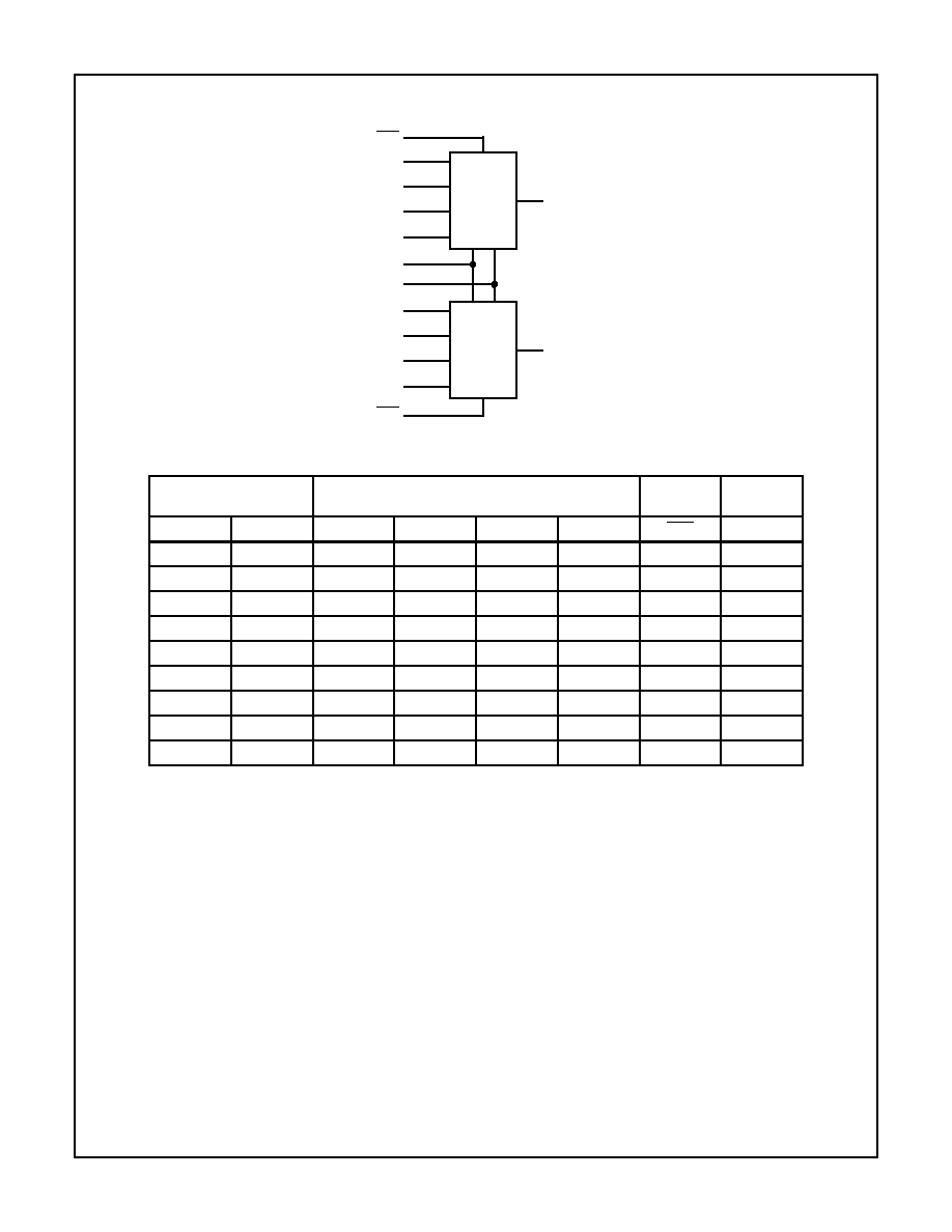
Functional Diagram
TRUTH TABLE
SELECT INPUTS
DATA INPUTS
ENABLE
INPUTS
OUTPUT
S1
S0
nI
0
nI
1
nI
2
nI
3
nOE
nY
X
X
X
X
X
X
H
Z
L
L
L
X
X
X
L
L
L
L
H
X
X
X
L
H
L
H
X
L
X
X
L
L
L
H
X
H
X
X
L
H
H
L
X
X
L
X
L
L
H
L
X
X
H
X
L
H
H
H
X
X
X
L
L
L
H
H
X
X
X
H
L
H
Select inputs S1 and S0 are common to both sections. H = High level, L = Low inputs, X = Don't care, Z = High imped-
ance.
GND = 8
V
CC
= 16
1I
2
4
3
1I
3
1I
1
5
1I
0
6
1
14
2
2I
2
12
13
2I
3
2I
1
11
2I
0
10
15
1OE
S0
S1
2OE
SEL/MUX
SEL/MUX
9
7
1Y
2Y
CD74AC253, CD54/74ACT253
3
Absolute Maximum Ratings
Thermal Information
DC Supply Voltage, V
CC
. . . . . . . . . . . . . . . . . . . . . . . . -0.5V to 6V
DC Input Diode Current, I
IK
For V
I
< -0.5V or V
I
> V
CC
+ 0.5V
. . . . . . . . . . . . . . . . . . . . . .±
20mA
DC Output Diode Current, I
OK
For V
O
< -0.5V or V
O
> V
CC
+ 0.5V
. . . . . . . . . . . . . . . . . . . .±
50mA
DC Output Source or Sink Current per Output Pin, I
O
For V
O
> -0.5V or V
O
< V
CC
+ 0.5V
. . . . . . . . . . . . . . . . . . . .±
50mA
DC V
CC
or Ground Current, I
CC or
I
GND
(Note 3)
. . . . . . . . .±
100mA
Operating Conditions
Temperature Range, T
A
. . . . . . . . . . . . . . . . . . . . . . -55
o
C to 125
o
C
Supply Voltage Range, V
CC
(Note 4)
AC Types. . . . . . . . . . . . . . . . . . . . . . . . . . . . . . . . . . .1.5V to 5.5V
ACT Types . . . . . . . . . . . . . . . . . . . . . . . . . . . . . . . . .4.5V to 5.5V
DC Input or Output Voltage, V
I
, V
O
. . . . . . . . . . . . . . . . . 0V to V
CC
Input Rise and Fall Slew Rate, dt/dv
AC Types, 1.5V to 3V . . . . . . . . . . . . . . . . . . . . . . . . . 50ns (Max)
AC Types, 3.6V to 5.5V . . . . . . . . . . . . . . . . . . . . . . . . 20ns (Max)
ACT Types, 4.5V to 5.5V. . . . . . . . . . . . . . . . . . . . . . . 10ns (Max)
Thermal Resistance (Typical, Note 5)
JA
(
o
C/W)
PDIP Package . . . . . . . . . . . . . . . . . . . . . . . . . . . . .
___
SOIC Package . . . . . . . . . . . . . . . . . . . . . . . . . . . . .
___
Maximum Junction Temperature (Plastic Package) . . . . . . . . . . . 150C
Maximum Storage Temperature Range . . . . . . . . . .-65
o
C to 150
o
C
Maximum Lead Temperature (Soldering 10s) . . . . . . . . . . . . . 300
o
C
CAUTION: Stresses above those listed in "Absolute Maximum Ratings" may cause permanent damage to the device. This is a stress only rating and operation
of the device at these or any other conditions above those indicated in the operational sections of this specification is not implied.
NOTES:
3. For up to 4 outputs per device, add
±
25mA for each additional output.
4. Unless otherwise specified, all voltages are referenced to ground.
5.
JA
is measured with the component mounted on an evaluation PC board in free air.
DC Electrical Specifications
PARAMETER
SYMBOL
TEST
CONDITIONS
V
CC
(V)
25
o
C
-40
o
C TO
85
o
C
-55
o
C TO
125
o
C
UNITS
V
I
(V)
I
O
(mA)
MIN
MAX
MIN
MAX
MIN
MAX
AC TYPES
High Level Input Voltage
V
IH
-
-
1.5
1.2
-
1.2
-
1.2
-
V
3
2.1
-
2.1
-
2.1
-
V
5.5
3.85
-
3.85
-
3.85
-
V
Low Level Input Voltage
V
IL
-
-
1.5
-
0.3
-
0.3
-
0.3
V
3
-
0.9
-
0.9
-
0.9
V
5.5
-
1.65
-
1.65
-
1.65
V
High Level Output Voltage
V
OH
V
IH
or V
IL
-0.05
1.5
1.4
-
1.4
-
1.4
-
V
-0.05
3
2.9
-
2.9
-
2.9
-
V
-0.05
4.5
4.4
-
4.4
-
4.4
-
V
-4
3
2.58
-
2.48
-
2.4
-
V
-24
4.5
3.94
-
3.8
-
3.7
-
V
-75
(Note 6, 7)
5.5
-
-
3.85
-
-
-
V
-50
(Note 6, 7)
5.5
-
-
-
-
3.85
-
V
CD74AC253, CD54/74ACT253
4
Low Level Output Voltage
V
OL
V
IH
or V
IL
0.05
1.5
-
0.1
-
0.1
-
0.1
V
0.05
3
-
0.1
-
0.1
-
0.1
V
0.05
4.5
-
0.1
-
0.1
-
0.1
V
12
3
-
0.36
-
0.44
-
0.5
V
24
4.5
-
0.36
-
0.44
-
0.5
V
75
(Note 6, 7)
5.5
-
-
-
1.65
-
-
V
50
(Note 6, 7)
5.5
-
-
-
-
-
1.65
V
Input Leakage Current
I
I
V
CC
or
GND
-
5.5
-
±
0.1
-
±
1
-
±
1
µ
A
Three-State Leakage
Current
I
OZ
V
IH
or V
IL
V
O
= V
CC
or GND
-
5.5
-
±
0.5
-
±
5
-
±
10
µ
A
Quiescent Supply Current
MSI
I
CC
V
CC
or
GND
0
5.5
-
8
-
80
-
160
µ
A
ACT TYPES
High Level Input Voltage
V
IH
-
-
4.5 to
5.5
2
-
2
-
2
-
V
Low Level Input Voltage
V
IL
-
-
4.5 to
5.5
-
0.8
-
0.8
-
0.8
V
High Level Output Voltage
V
OH
V
IH
or V
IL
-0.05
4.5
4.4
-
4.4
-
4.4
-
V
-24
4.5
3.94
-
3.8
-
3.7
-
V
-75
(Note 6, 7)
5.5
-
-
3.85
-
-
-
V
-50
(Note 6, 7)
5.5
-
-
-
-
3.85
-
V
Low Level Output Voltage
V
OL
V
IH
or V
IL
0.05
4.5
-
0.1
-
0.1
-
0.1
V
24
4.5
-
0.36
-
0.44
-
0.5
V
75
(Note 6, 7)
5.5
-
-
-
1.65
-
-
V
50
(Note 6, 7)
5.5
-
-
-
-
-
1.65
V
Input Leakage Current
I
I
V
CC
or
GND
-
5.5
-
±
0.1
-
±
1
-
±
1
µ
A
Three-State or Leakage
Current
I
OZ
V
IH
or V
IL
V
O
= V
CC
or GND
-
5.5
-
±
0.5
-
±
5
-
±
10
µ
A
Quiescent Supply Current
MSI
I
CC
V
CC
or
GND
0
5.5
-
8
-
80
-
160
µ
A
Additional Supply Current per
Input Pin TTL Inputs High
1 Unit Load
I
CC
V
CC
-2.1
-
4.5 to
5.5
-
2.4
-
2.8
-
3
mA
NOTES:
6. Test one output at a time for a 1-second maximum duration. Measurement is made by forcing current and measuring voltage to minimize
power dissipation.
7. Test verifies a minimum 50
transmission-line-drive capability at 85
o
C, 75
at 125
o
C.
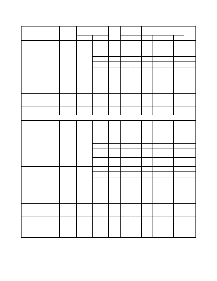
DC Electrical Specifications
(Continued)
PARAMETER
SYMBOL
TEST
CONDITIONS
V
CC
(V)
25
o
C
-40
o
C TO
85
o
C
-55
o
C TO
125
o
C
UNITS
V
I
(V)
I
O
(mA)
MIN
MAX
MIN
MAX
MIN
MAX
CD74AC253, CD54/74ACT253
5
ACT Input Load Table
INPUT
UNIT LOAD
S0, S1, nI
0
, nI
1
1
nOE
0.83
NOTE: Unit load is
I
CC
limit specified in DC Electrical Specifications
Table, e.g., 2.4mA max at 25
o
C.
Switching Specifications
Input t
r
, t
f
= 3ns, C
L
= 50pF (Worst Case)
PARAMETER
SYMBOL
V
CC
(V)
-40
o
C TO 85
o
C
-55
o
C TO 125
o
C
UNITS
MIN
TYP
MAX
MIN
TYP
MAX
AC TYPES
Propagation Delay,
S0, S1, to Y
t
PLH
, t
PHL
1.5
-
-
227
-
-
250
ns
3.3
(Note 9)
7.2
-
25
7
-
28
ns
5
(Note 10)
5.2
-
18.2
5
-
20
ns
Propagation Delay,
nI to Y
t
PLH
, t
PHL
1.5
-
-
151
-
-
166
ns
3.3
4.8
-
16.9
4.7
-
18.6
ns
5
3.4
-
12.1
3.3
-
13.3
ns
Propagation Delay,
Output Enable,
Output Disable to Y
t
PLZ
, t
PHZ
,
t
PZL
, t
PZH
1.5
-
-
131
-
-
144
ns
3.3
4.5
-
15.7
4.3
-
17.3
ns
5
3
-
10.5
2.9
-
11.5
ns
Three-State Output
Capacitance
C
O
-
-
-
15
-
-
15
pF
Input Capacitance
C
I
-
-
-
10
-
-
10
pF
Power Dissipation Capacitance
C
PD
(Note 11)
-
-
107
-
-
107
-
pF
ACT TYPES
Propagation Delay,
S0, S1, to Y
t
PLH
, t
PHL
5
(Note 10)
5.7
-
20
5.5
-
22
ns
Propagation Delay,
nI to Y
t
PLH
, t
PHL
5
4.6
-
16.4
4.5
-
18
ns
Propagation Delay,
Output Enable,
Output Disable to Y
t
PLZ
, t
PHZ
,
t
PZL
, t
PZH
5
3.2
-
11.5
3.2
-
12.6
ns
Three-State Output
Capacitance
C
O
-
-
-
15
-
-
15
pF
Input Capacitance
C
I
-
-
-
10
-
-
10
pF
Power Dissipation Capacitance
C
PD
(Note 11)
-
-
107
-
-
107
-
pF
NOTES:
8. Limits tested 100%.
9. 3.3V Min is at 3.6V, Max is at 3V.
10. 5V Min is at 5.5V, Max is at 4.5V.
11. C
PD
is used to determine the dynamic power consumption per multiplexer.
AC: P
D
= V
CC
2
f
i
(C
PD
+ C
L
)
ACT: P
D
= V
CC
2
f
i
(C
PD
+ C
L
) + V
CC
I
CC
where f
i
= input frequency, C
L
= output load capacitance, V
CC
= supply voltage.
CD74AC253, CD54/74ACT253