CD74AC86
QUADRUPLE 2-INPUT EXCLUSIVE-OR GATE
SCHS324 ≠ JANUARY 2003
1
POST OFFICE BOX 655303
∑
DALLAS, TEXAS 75265
D
AC Types Feature 1.5-V to 5.5-V Operation
and Balanced Noise Immunity at 30% of the
Supply
D
Speed of Bipolar F, AS, and S, With
Significantly Reduced Power Consumption
D
Balanced Propagation Delays
D
±
24-mA Output Drive Current
≠ Fanout to 15 F Devices
D
SCR-Latchup-Resistant CMOS Process and
Circuit Design
D
Exceeds 2-kV ESD Protection Per
MIL-STD-883, Method 3015
description/ordering information
The CD74AC86 is a quadruple 2-input exclusive-OR gate. This device performs the Boolean function
Y = A
B or Y = AB + AB in positive logic.
A common application is as a true/complement element. If one of the inputs is low, the other input is reproduced
in true form at the output. If one of the inputs is high, the signal on the other input is reproduced inverted at the
output.
ORDERING INFORMATION
TA
PACKAGE
ORDERABLE
PART NUMBER
TOP-SIDE
MARKING
PDIP ≠ E
Tube
CD74AC86E
CD74AC86E
≠55
∞
C to 125
∞
C
SOIC ≠ M
Tube
CD74AC86M
AC86M
SOIC ≠ M
Tape and reel
CD74AC86M96
AC86M
Package drawings, standard packing quantities, thermal data, symbolization, and PCB design guidelines
are available at www.ti.com/sc/package.
FUNCTION TABLE
(each gate)
INPUTS
OUTPUT
A
B
Y
L
L
L
L
H
H
H
L
H
H
H
L
Copyright
2003, Texas Instruments Incorporated
PRODUCTION DATA information is current as of publication date.
Products conform to specifications per the terms of Texas Instruments
standard warranty. Production processing does not necessarily include
testing of all parameters.
Please be aware that an important notice concerning availability, standard warranty, and use in critical applications of
Texas Instruments semiconductor products and disclaimers thereto appears at the end of this data sheet.
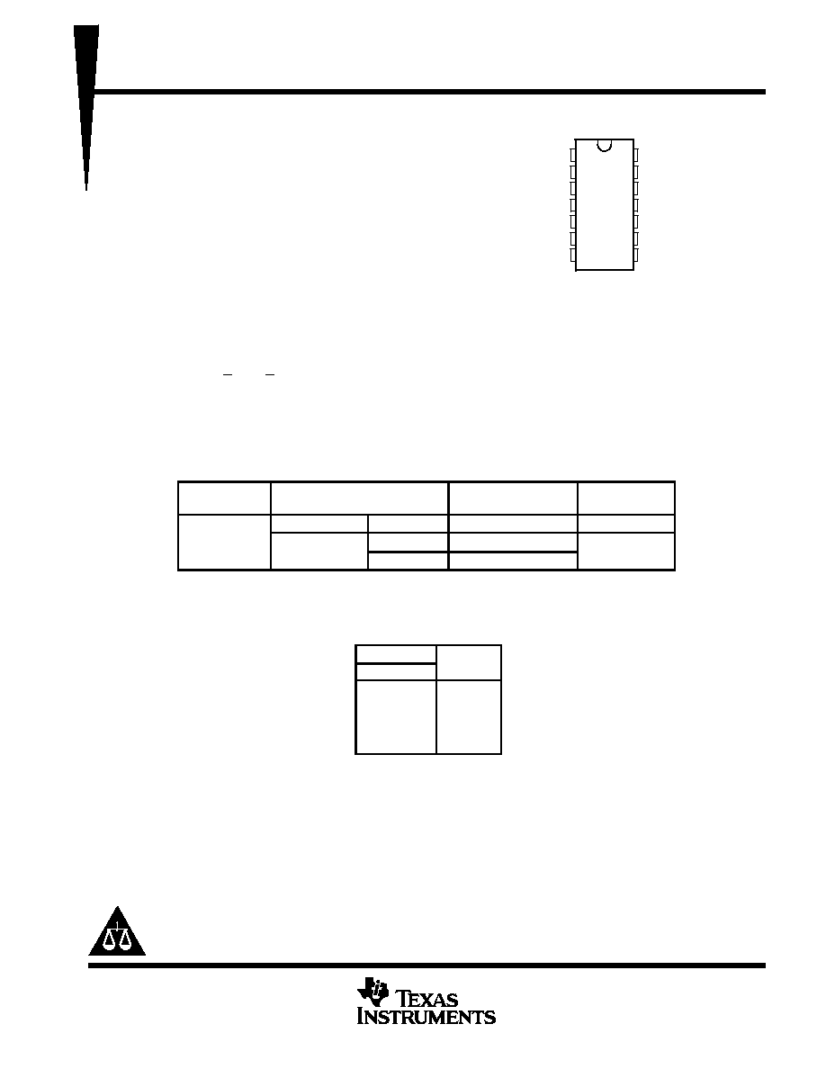
E OR M PACKAGE
(TOP VIEW)
1
2
3
4
5
6
7
14
13
12
11
10
9
8
1A
1B
1Y
2A
2B
2Y
GND
V
CC
4B
4A
4Y
3B
3A
3Y
CD74AC86
QUADRUPLE 2-INPUT EXCLUSIVE-OR GATE
SCHS324 ≠ JANUARY 2003
2
POST OFFICE BOX 655303
∑
DALLAS, TEXAS 75265
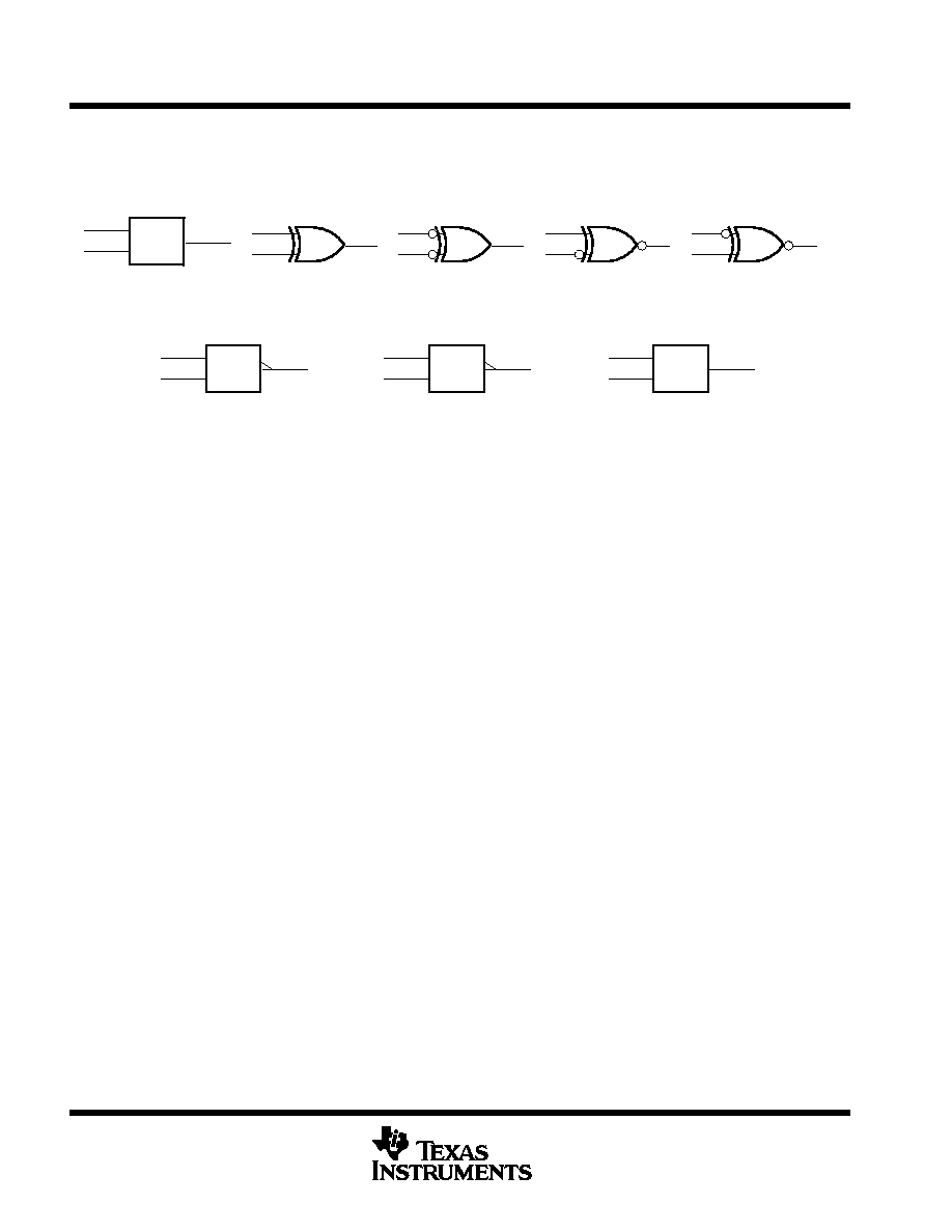
exclusive-OR logic
An exclusive-OR gate has many applications, some of which can be represented better by alternative
logic symbols.
= 1
EXCLUSIVE OR
These are five equivalent exclusive-OR symbols valid for an CD74AC86 gate in positive logic; negation may be shown at any two ports.
=
2k
2k + 1
LOGIC-IDENTITY ELEMENT
EVEN-PARITY ELEMENT
ODD-PARITY ELEMENT
The output is active (low) if
all inputs stand at the same
logic level (i.e., A = B).
The output is active (low) if
an even number of inputs
(i.e., 0 or 2) are active.
The output is active (high) if
an odd number of inputs
(i.e., only 1 of the 2) are
active.
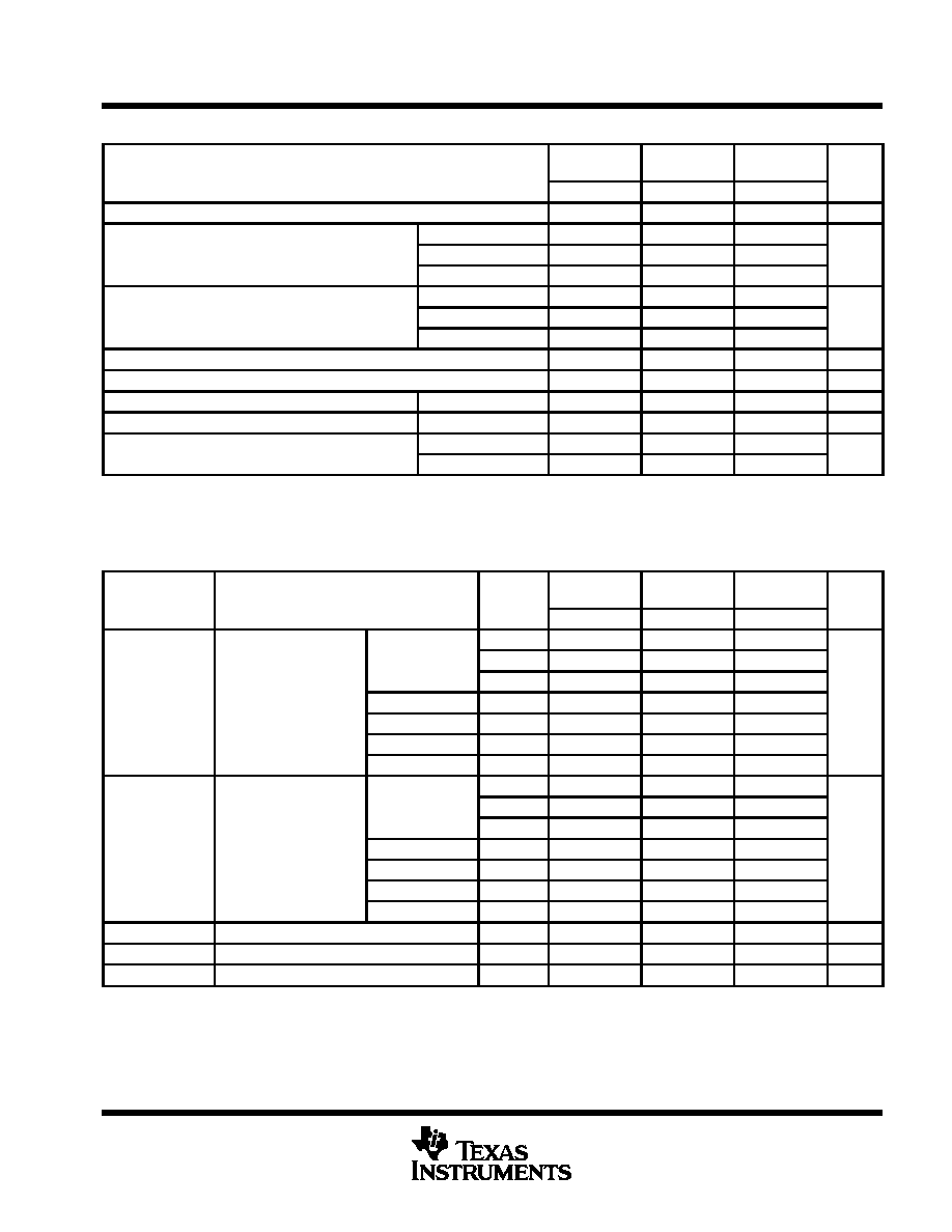
absolute maximum ratings over operating free-air temperature range (unless otherwise noted)
Supply voltage range, V
CC
≠ 0.5 V to 6 V
. . . . . . . . . . . . . . . . . . . . . . . . . . . . . . . . . . . . . . . . . . . . . . . . . . . . . . . . . .
Input clamp current, I
IK
(V
I
< 0 or V
I
> V
CC
) (see Note 1)
±
20 mA
. . . . . . . . . . . . . . . . . . . . . . . . . . . . . . . . . . . . .
Output clamp current, I
OK
(V
O
< 0 or V
O
> V
CC
) (see Note 1)
±
50 mA
. . . . . . . . . . . . . . . . . . . . . . . . . . . . . . . .
Continuous output current, I
O
(V
O
= 0 to V
CC
)
±
50 mA
. . . . . . . . . . . . . . . . . . . . . . . . . . . . . . . . . . . . . . . . . . . . . .
Continuous current through V
CC
or GND
±
100 mA
. . . . . . . . . . . . . . . . . . . . . . . . . . . . . . . . . . . . . . . . . . . . . . . . . .
Package thermal impedance,
JA
(see Note 2): E package
80
∞
C/W
. . . . . . . . . . . . . . . . . . . . . . . . . . . . . . . . . . .
M package
86
∞
C/W
. . . . . . . . . . . . . . . . . . . . . . . . . . . . . . . . . .
Storage temperature range, T
stg
≠ 65
∞
C to 150
∞
C
. . . . . . . . . . . . . . . . . . . . . . . . . . . . . . . . . . . . . . . . . . . . . . . . . . .
Stresses beyond those listed under "absolute maximum ratings" may cause permanent damage to the device. These are stress ratings only, and
functional operation of the device at these or any other conditions beyond those indicated under "recommended operating conditions" is not
implied. Exposure to absolute-maximum-rated conditions for extended periods may affect device reliability.
NOTES:
1. The input and output voltage ratings may be exceeded if the input and output current ratings are observed.
2. The package thermal impedance is calculated in accordance with JESD 51-7.
CD74AC86
QUADRUPLE 2-INPUT EXCLUSIVE-OR GATE
SCHS324 ≠ JANUARY 2003
3
POST OFFICE BOX 655303
∑
DALLAS, TEXAS 75265
recommended operating conditions (see Note 3)
TA = 25
∞
C
≠55
∞
C to
125
∞
C
≠40
∞
C to
85
∞
C
UNIT
MIN
MAX
MIN
MAX
MIN
MAX
VCC
Supply voltage
1.5
5.5
1.5
5.5
1.5
5.5
V
VCC = 1.5 V
1.2
1.2
1.2
VIH
High-level input voltage
VCC = 3 V
2.1
2.1
2.1
V
VCC = 5.5 V
3.85
3.85
3.85
VCC = 1.5 V
0.3
0.3
0.3
VIL
Low-level input voltage
VCC = 3 V
0.9
0.9
0.9
V
VCC = 5.5 V
1.65
1.65
1.65
VI
Input voltage
0
VCC
0
VCC
0
VCC
V
VO
Output voltage
0
VCC
0
VCC
0
VCC
V
IOH
High-level output current
VCC = 4.5 V to 5.5 V
≠24
≠24
≠24
mA
IOL
Low-level output current
VCC = 4.5 V to 5.5 V
24
24
24
mA
t/
v
Input transition rise or fall rate
VCC = 1.5 V to 3 V
50
50
50
ns/V
t/
v
Input transition rise or fall rate
VCC = 3.6 V to 5.5 V
20
20
20
ns/V
NOTE 3: All unused inputs of the device must be held at VCC or GND to ensure proper device operation. Refer to the TI application report,
Implications of Slow or Floating CMOS Inputs, literature number SCBA004.
electrical characteristics over recommended operating free-air temperature range (unless
otherwise noted)
PARAMETER
TEST CONDITIONS
VCC
TA = 25
∞
C
≠55
∞
C to
125
∞
C
≠40
∞
C to
85
∞
C
UNIT
CC
MIN
MAX
MIN
MAX
MIN
MAX
1.5 V
1.4
1.4
1.4
IOH = ≠50
µ
A
3 V
2.9
2.9
2.9
4.5 V
4.4
4.4
4.4
VOH
VI = VIH or VIL
IOH = ≠4 mA
3 V
2.58
2.4
2.48
V
IOH = ≠24 mA
4.5 V
3.94
3.7
3.8
IOH = ≠50 mA
5.5 V
3.85
IOH = ≠75 mA
5.5 V
3.85
1.5 V
0.1
0.1
0.1
IOL = 50
µ
A
3 V
0.1
0.1
0.1
4.5 V
0.1
0.1
0.1
VOL
VI = VIH or VIL
IOL = 12 mA
3 V
0.36
0.5
0.44
V
IOL = 24 mA
4.5 V
0.36
0.5
0.44
IOL = 50 mA
5.5 V
1.65
IOL = 75 mA
5.5 V
1.65
II
VI = VCC or GND
5.5 V
±
0.1
±
1
±
1
µ
A
ICC
VI = VCC or GND,
IO = 0
5.5 V
4
80
40
µ
A
Ci
10
10
10
pF
Test one output at a time, not exceeding 1-second duration. Measurement is made by forcing indicated current and measuring voltage to minimize
power dissipation. Test verifies a minimum 50-
transmission-line drive capability at 85
∞
C and 75-
transmission-line drive capability at 125
∞
C.
CD74AC86
QUADRUPLE 2-INPUT EXCLUSIVE-OR GATE
SCHS324 ≠ JANUARY 2003
4
POST OFFICE BOX 655303
∑
DALLAS, TEXAS 75265
switching characteristics over recommended operating free-air temperature range,
V
CC
= 1.5 V, C
L
= 50 pF (unless otherwise noted) (see Figure 1)
PARAMETER
FROM
(INPUT)
TO
(OUTPUT)
≠55
∞
C to
125
∞
C
≠40
∞
C TO
85
∞
C
UNIT
(INPUT)
(OUTPUT)
MIN
MAX
MIN
MAX
tPLH
A or B
Y
135
123
ns
tPHL
A or B
Y
135
123
ns
switching characteristics over recommended operating free-air temperature range,
V
CC
= 3 V
±
0.3 V, C
L
= 50 pF (unless otherwise noted) (see Figure 1)
PARAMETER
FROM
(INPUT)
TO
(OUTPUT)
≠55
∞
C to
125
∞
C
≠40
∞
C TO
85
∞
C
UNIT
(INPUT)
(OUTPUT)
MIN
MAX
MIN
MAX
tPLH
A or B
Y
3.8
15.1
3.9
13.7
ns
tPHL
A or B
Y
3.8
15.1
3.9
13.7
ns
switching characteristics over recommended operating free-air temperature range,
V
CC
= 5 V
±
0.5 V, C
L
= 50 pF (unless otherwise noted) (see Figure 1)
PARAMETER
FROM
(INPUT)
TO
(OUTPUT)
≠55
∞
C to
125
∞
C
≠40
∞
C TO
85
∞
C
UNIT
(INPUT)
(OUTPUT)
MIN
MAX
MIN
MAX
tPLH
A or B
Y
2.7
10.8
2.8
9.8
ns
tPHL
A or B
Y
2.7
10.8
2.8
9.8
ns
operating characteristics, T
A
= 25
∞
C
PARAMETER
TYP
UNIT
Cpd
Power dissipation capacitance
57
pF
CD74AC86
QUADRUPLE 2-INPUT EXCLUSIVE-OR GATE
SCHS324 ≠ JANUARY 2003
5
POST OFFICE BOX 655303
∑
DALLAS, TEXAS 75265
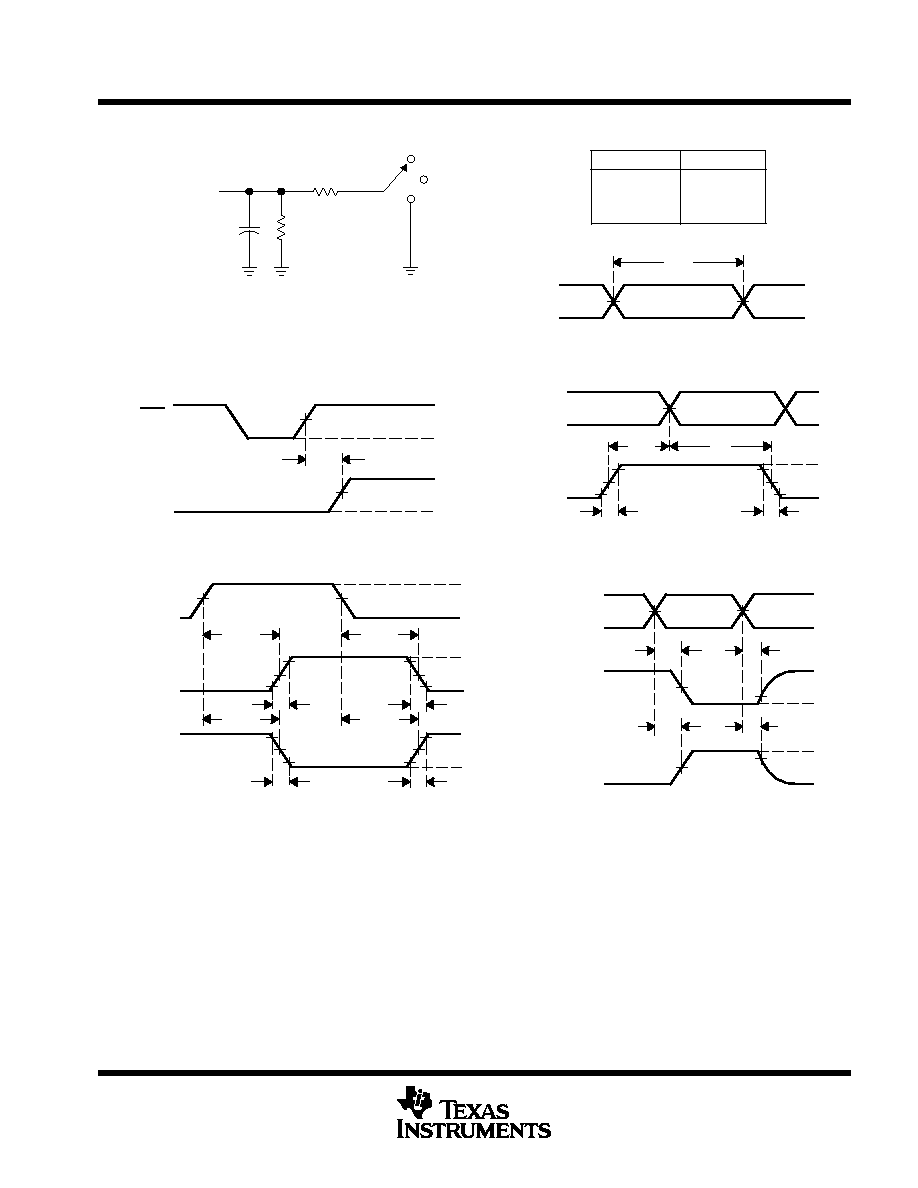
PARAMETER MEASUREMENT INFORMATION
VOLTAGE WAVEFORMS
SETUP AND HOLD AND INPUT RISE AND FALL TIMES
th
tsu
50% VCC
50% VCC
50%
10%
10%
90%
90%
VCC
VCC
0 V
0 V
tr
tf
Reference
Input
Data
Input
VOLTAGE WAVEFORMS
PROPAGATION DELAY AND OUTPUT TRANSITION TIMES
50% VCC
50% VCC
50%
10%
10%
90%
90%
VCC
VOH
VOL
0 V
tr
tf
Input
In-Phase
Output
50% VCC
tPLH
tPHL
50% VCC
50%
10%
10%
90%
90%
VOH
VOL
tr
tf
tPHL
tPLH
Out-of-Phase
Output
NOTES: A. CL includes probe and test-fixture capacitance.
B. Waveform 1 is for an output with internal conditions such that the output is low except when disabled by the output control.
Waveform 2 is for an output with internal conditions such that the output is high except when disabled by the output control.
C. All input pulses are supplied by generators having the following characteristics: PRR
1 MHz, ZO = 50
, tr = 3 ns, tf = 3 ns.
Phase relationships between waveforms are arbitrary.
D. For clock inputs, fmax is measured with the input duty cycle at 50%.
E. The outputs are measured one at a time with one input transition per measurement.
F. tPLH and tPHL are the same as tpd.
G. tPZL and tPZH are the same as ten.
H. tPLZ and tPHZ are the same as tdis.
I. All parameters and waveforms are not applicable to all devices.
From Output
Under Test
CL = 50 pF
(see Note A)
LOAD CIRCUIT
S1
2
◊
VCC
R1 = 500
Open
GND
0 V
tw
VOLTAGE WAVEFORMS
PULSE DURATION
Input
50% VCC
50% VCC
VCC
tPLH/tPHL
tPLZ/tPZL
tPHZ/tPZH
Open
2
◊
VCC
GND
TEST
S1
Output
Control
Output
Waveform 1
S1 at 2
◊
VCC
(see Note B)
Output
Waveform 2
S1 at GND
(see Note B)
VOL
VOH
tPZL
tPZH
tPLZ
tPHZ
VCC
0 V
50% VCC
20% VCC
50% VCC
0 V
VOLTAGE WAVEFORMS
OUTPUT ENABLE AND DISABLE TIMES
50% VCC
50% VCC
80% VCC
VCC
R2 = 500
When VCC = 1.5 V, R1 = R2 = 1 k
VOLTAGE WAVEFORMS
RECOVERY TIME
50% VCC
VCC
0 V
CLR
Input
CLK
50% VCC
VCC
trec
0 V
Figure 1. Load Circuit and Voltage Waveforms