CD74ACT297
DIGITAL PHASE-LOCKED LOOP
SCHS297D ≠ AUGUST 1998 ≠ REVISED JUNE 2002
1
POST OFFICE BOX 655303
∑
DALLAS, TEXAS 75265
D
Speed of Bipolar FCT, AS, and S, With
Significantly Reduced Power Consumption
D
Digital Design Avoids Analog
Compensation Errors
D
Easily Cascadable for Higher-Order Loops
D
Useful Frequency Range
≠ DC to 110 MHz Typical (K CLK)
≠ DC to 70 MHz Typical (I/D CLK)
D
Dynamically Variable Bandwidth
D
Very Narrow Bandwidth Attainable
D
Power-On Reset
D
Output Capability
≠ Standard: XORPD OUT, ECPD OUT
≠ Bus Driver: I/D OUT
D
SCR Latch-Up-Resistant CMOS Process
and Circuit Design
D
Balanced Propagation Delays
D
ESD Protection Exceeds 2000 V Per
MIL-STD-883, Method 3015
description/ordering information
The CD74ACT297 provides a simple, cost-effective solution to high-accuracy, digital, phase-locked-loop
applications. This device contains all the necessary circuits, with the exception of the divide-by-N counter, to
build first-order phase-locked loops as shown in Figure 1.
Both exclusive-OR phase detectors (XORPDs) and edge-controlled (ECPD) phase detectors are provided for
maximum flexibility.
Proper partitioning of the loop function, with many of the building blocks external to the package, makes it easy
for the designer to incorporate ripple cancellation or to cascade to higher-order phase-locked loops.
The length of the up/down K counter is digitally programmable according to the K-counter function table. With
A, B, C, and D all low, the K counter is disabled. With A high and B, C, and D low, the K counter is only three
stages long, which widens the bandwidth, or capture range, and shortens the lock time of the loop. When A,
B, C, and D are programmed high, the K counter becomes 17 stages long, which narrows the bandwidth, or
capture range, and lengthens the lock time. Real-time control of loop bandwidth by manipulating the
A-through-D inputs can maximize the overall performance of the digital phase-locked loop.
ORDERING INFORMATION
TA
PACKAGE
ORDERABLE
PART NUMBER
TOP-SIDE
MARKING
55
∞
C to 125
∞
C
SOIC
M
Tube
CD74ACT297M
ACT297M
≠55
∞
C to 125
∞
C
SOIC ≠ M
Tape and reel
CD74ACT297M96
ACT297M
Package drawings, standard packing quantities, thermal data, symbolization, and PCB design
guidelines are available at www.ti.com/sc/package.
Copyright
2002, Texas Instruments Incorporated
PRODUCTION DATA information is current as of publication date.
Products conform to specifications per the terms of Texas Instruments
standard warranty. Production processing does not necessarily include
testing of all parameters.
Please be aware that an important notice concerning availability, standard warranty, and use in critical applications of
Texas Instruments semiconductor products and disclaimers thereto appears at the end of this data sheet.
1
2
3
4
5
6
7
8
16
15
14
13
12
11
10
9
B
A
ENCTR
K CLK
I/D CLK
D/U
I/D OUT
GND
V
CC
C
D
A2
ECPD OUT
XORPD OUT
B
A1
M PACKAGE
(TOP VIEW)
CD74ACT297
DIGITAL PHASE-LOCKED LOOP
SCHS297D ≠ AUGUST 1998 ≠ REVISED JUNE 2002
2
POST OFFICE BOX 655303
∑
DALLAS, TEXAS 75265
description/ordering information (continued)
This device performs the classic first-order phase-locked-loop function without using analog components. The
accuracy of the digital phase-locked loop (DPLL) is not affected by V
CC
and temperature variations, but depends
solely on accuracies of the K clock (K CLK), increment/decrement clock (I/D CLK), and loop propagation delays.
The I/D clock frequency and the divide-by-N modulos determine the center frequency of the DPLL. The center
frequency is defined by the relationship f
c
= I/D clock/2N (Hz).
Increment/Decrement
Circuit
Modulo K
Counter
K CLK
I/D CLK
B
A2
D/U
ENCTR
A1
D C
B
A
14 15 1
2
4
6
3
5
9
10
13
7
11
12
J
K
ECPD OUT
XORPD OUT
I/D OUT
Modulo Controls
Figure 1. Simplified Block Diagram
CD74ACT297
DIGITAL PHASE-LOCKED LOOP
SCHS297D ≠ AUGUST 1998 ≠ REVISED JUNE 2002
3
POST OFFICE BOX 655303
∑
DALLAS, TEXAS 75265
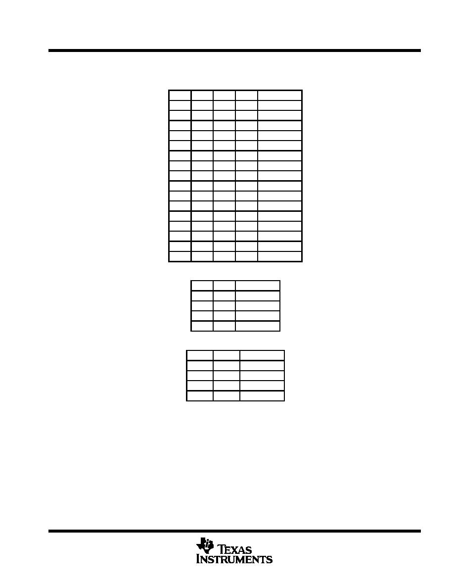
Function Tables
K COUNTER
(digital control)
D
C
B
A
MODULO (K)
L
L
L
L
Inhibited
L
L
L
H
23
L
L
H
L
24
L
L
H
H
25
L
H
L
L
26
L
H
L
H
27
L
H
H
L
28
L
H
H
H
29
H
L
L
L
210
H
L
L
H
211
H
L
H
L
212
H
L
H
H
213
H
H
L
L
214
H
H
L
H
215
H
H
H
L
216
H
H
H
H
217
EXCLUSIVE-OR PHASE DETECTOR
A1
B
XORPD OUT
L
L
L
L
H
H
H
L
H
H
H
L
EDGE-CONTROLLED PHASE DETECTOR
A2
B
ECPD OUT
H or L
H
H or L
L
H or L
No change
H or L
No change
H = steady-state high level
L = steady-state low level
= transition from high to low
= transition from low to high
CD74ACT297
DIGITAL PHASE-LOCKED LOOP
SCHS297D ≠ AUGUST 1998 ≠ REVISED JUNE 2002
4
POST OFFICE BOX 655303
∑
DALLAS, TEXAS 75265
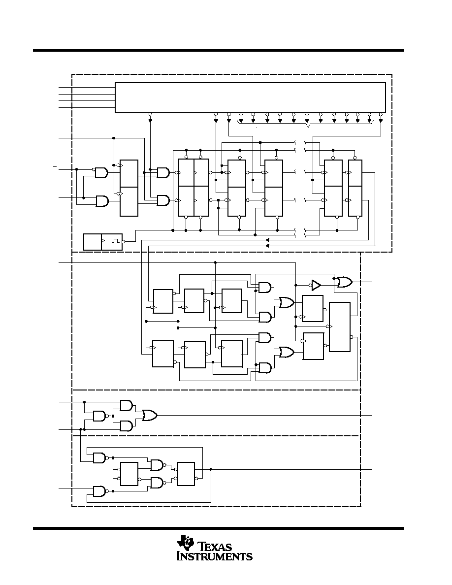
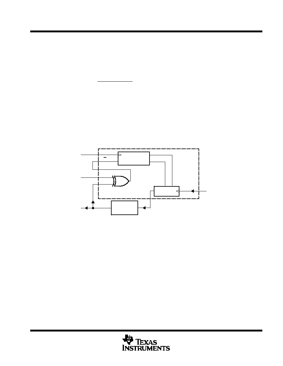
functional block diagram
D/U
To Mode Controls 12≠2 (11 stages not shown)
2
1
15
14
4
6
3
5
9
10
13
7
8
9
10
11
12
13
14
0
1
2
4
8
2
1
A
B
C
D
4
6
3
5
K CLK
ENCTR
I/D CLK
I/D OUT
Power-Up Reset
l = 1
C20
20D
XORPD OUT
ECPD OUT
R
14D
14T
M14
13D
M13
1T
Increment
R
R
R
R
R
T
T
T
1T
T
13T
13T
20D
C20
T
T
14D
14T
M13
13D
R
R
R
R
M14
R
R
I/D Circuit
Decrement
7
11
12
R
R
S
S
C21
C21
C21
C21
C21
C21
C21
C21
C21
21D
21D
21D
21D
21D
21D
21D
21D
Exclusive-OR Phase Detector
Edge-Controlled Phase Detector
A1
B
A2
1
X/Y
K Counter
21J
21K
CD74ACT297
DIGITAL PHASE-LOCKED LOOP
SCHS297D ≠ AUGUST 1998 ≠ REVISED JUNE 2002
5
POST OFFICE BOX 655303
∑
DALLAS, TEXAS 75265
detailed description
The phase detector generates an error-signal waveform that, at zero phase error, is a 50% duty-cycle square wave.
At the limits of linear operation, the phase-detector output is either high or low all of the time, depending on the
direction of the phase error (
in
≠
out
). Within these limits, the phase-detector output varies linearly with the input
phase error according to the gain k
d
, which is expressed in terms of phase-detector output per cycle of phase error.
The phase-detector output can be varied between
±
1 according to the relation:
Phase-detector output
+
% high ≠ % low
100
The output of the phase detector is k
d
e
, where the phase error
e
=
in
≠
out
.
XORPD and ECPD are commonly used digital types. The ECPD is more complex than the XORPD, but can be
described generally as a circuit that changes states on one of the transitions of its inputs. For an XORPD, k
d
= 4,
because its output remains high (PD output = 1) for a phase error of one-fourth cycle. Similarly, for the ECPD,
k
d
= 2, because its output remains high for a phase error of one-half cycle. The type of phase detector determines
the zero-phase-error point, i.e., the phase separation of the phase-detector inputs for
e
is defined to be zero. For
the basic DPLL system of Figure 2,
e
= 0 when the phase-detector output is a square wave. The XORPD inputs are
one-fourth cycle out of phase for zero phase error. For the ECPD,
e
= 0 when the inputs are one-half cycle out of
phase.
D/U
B
A1
Divide-by-N
Counter
Divide-by-K
Counter
fin,
in
Mfc
I/D Circuit
I/D OUT
I/D CLK
Carry
Borrow
K CLK
XORPD OUT
fout,
out
2Nfc
Figure 2. DPLL Using Exclusive-OR Phase Detection
The phase-detector output controls the up/down input to the K counter. The counter is clocked by input frequency
Mf
c
, which is a multiple M of the loop center frequency f
c
. When the K counter recycles up, it generates a carry pulse.
Recycling while counting down generates a borrow pulse. If the carry and borrow outputs are conceptually combined
into one output that is positive for a carry and negative for a borrow, and if the K counter is considered as a frequency
divider with the ratio Mf
c
/K, the output of the K counter equals the input frequency multiplied by the division ratio. Thus,
the output from the K counter is k
d
e
Mf
c
/K.
The carry and borrow pulses go to the increment/decrement (I/D) circuit, which, in the absence of any carry or borrow
pulse, has an output that is one-half of the input clock (I/D CLK). The input clock is just a multiple (2N) of the loop
center frequency. In response to a carry or borrow pulse, the I/D circuit either adds or deletes a pulse at I/D OUT. Thus,
the output of the I/D circuit is Nf
c
+ (k
d
e
Mf
c
)/2K.
The output of the N counter (or the output of the phase-locked loop) is:
fo
+
fc
)
(k
d
f
eMfc) 2KN
When this result is compared to the equation for a first-order analog phase-locked loop, the digital equivalent of the
gain of the VCO is Mf
c
/2KN, or f
c
/K for M = 2N.
(1)
(2)