CD74FCT244, CD74FCT244AT
BiCMOS OCTAL BUFFERS/LINE DRIVERS
WITH 3-STATE OUTPUTS
SCBS722B ≠ JULY 2000 ≠ REVISED AUGUST 2003
1
POST OFFICE BOX 655303
∑
DALLAS, TEXAS 75265
D
BiCMOS Technology With Low Quiescent
Power
D
Buffered Inputs
D
Noninverted Outputs
D
Input/Output Isolation From V
CC
D
Controlled Output Edge Rates
D
64-mA Output Sink Current
D
Output Voltage Swing Limited to 3.7 V
D
SCR Latch-Up-Resistant BiCMOS Process
and Circuit Design
description/ordering information
The CD74FCT244 and CD74FCT244AT are octal
buffer/line drivers with 3-state outputs using a
small-geometry BiCMOS technology. The output stages are a combination of bipolar and CMOS transistors that
limit the output high level to two diode drops below V
CC
. This resultant lowering of output swing (0 V to 3.7 V)
reduces the power-bus ringing [a source of electromagnetic interference (EMI)] and minimizes V
CC
bounce and
ground bounce and their effects during simultaneous output switching. The output configuration also enhances
switching speed and is capable of sinking 64 mA.
These devices are organized as two 4-bit buffers/line drivers with separate active-low output-enable (OE)
inputs. When OE is low, the device passes data from the A inputs to the Y outputs. When OE is high, the outputs
are in the high-impedance state.
To ensure the high-impedance state during power up or power down, OE should be tied to V
CC
through a pullup
resistor; the minimum value of the resistor is determined by the current-sinking capability of the driver.
ORDERING INFORMATION
TA
PACKAGE
ORDERABLE
PART NUMBER
TOP-SIDE
MARKING
0 C to 70 C
PDIP ≠ E
Tube
CD74FCT244E
CD74FCT244E
0 C to 70 C
SOIC ≠ M
Tube
CD74FCT244M
74FCT244M
0 C to 70 C
SOIC ≠ M
Tape and reel
CD74FCT244M96
74FCT244M
0
∞
C to 70
∞
C
SSOP ≠ SM
Tape and reel
CD74FCT244SM96
FCT244SM
PDIP ≠ E
Tube
CD74FCT244ATE
CD74FCT244ATE
SOIC ≠ M
Tube
CD74FCT244ATM
74FCT244ATM
SOIC ≠ M
Tape and reel
CD74FCT244ATM96
74FCT244ATM
Package drawings, standard packing quantities, thermal data, symbolization, and PCB design
guidelines are available at www.ti.com/sc/package.
FUNCTION TABLE
(each buffer/driver)
INPUTS
OUTPUT
OE
A
OUTPUT
Y
L
H
H
L
L
L
H
X
Z
Copyright
2003, Texas Instruments Incorporated
PRODUCTION DATA information is current as of publication date.
Products conform to specifications per the terms of Texas Instruments
standard warranty. Production processing does not necessarily include
testing of all parameters.
Please be aware that an important notice concerning availability, standard warranty, and use in critical applications of
Texas Instruments semiconductor products and disclaimers thereto appears at the end of this data sheet.
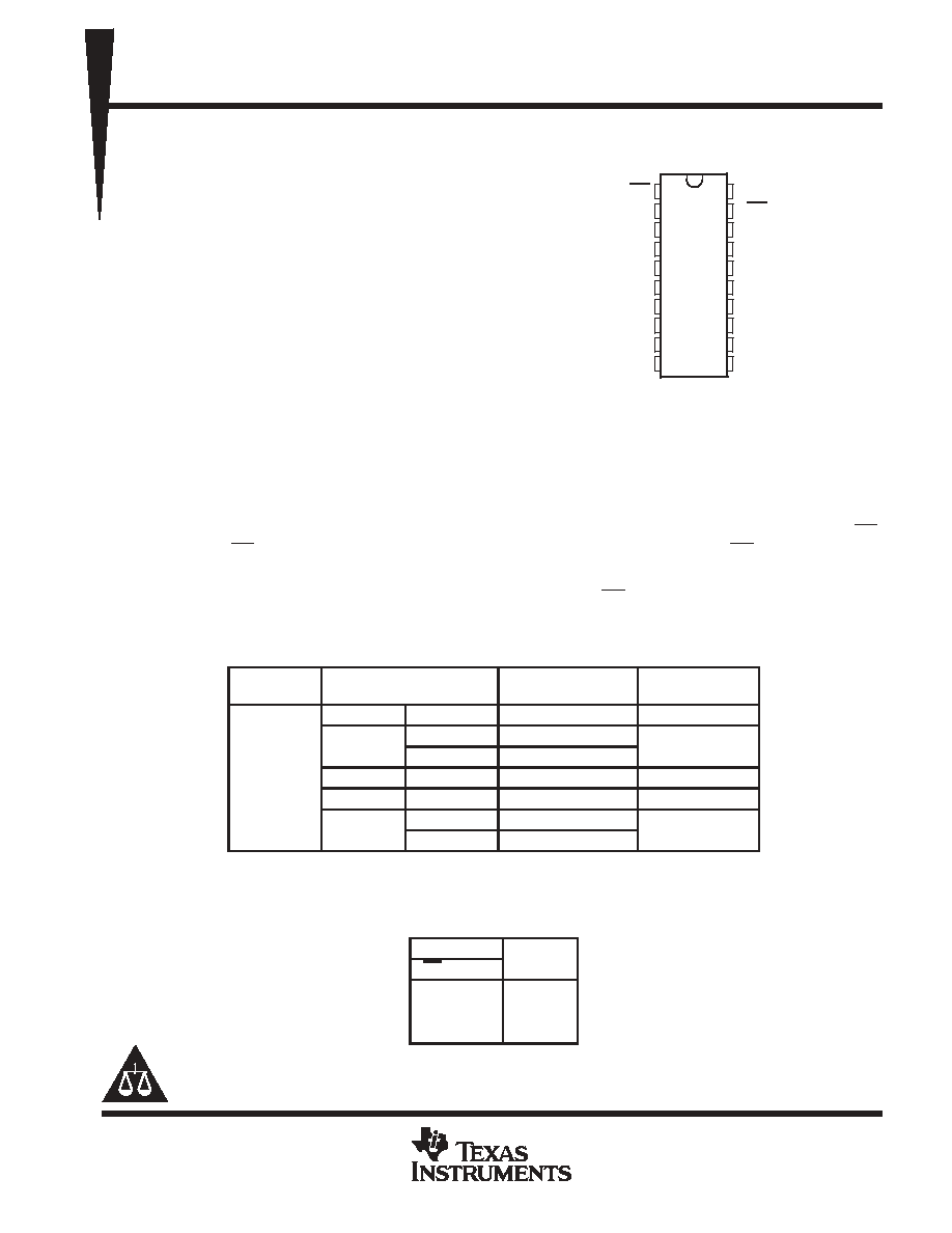
CD74FCT244 . . . E, M, OR SM PACKAGE
CD74FCT244AT . . . E OR M PACKAGE
(TOP VIEW)
1
2
3
4
5
6
7
8
9
10
20
19
18
17
16
15
14
13
12
11
1OE
1A1
2Y4
1A2
2Y3
1A3
2Y2
1A4
2Y1
GND
V
CC
2OE
1Y1
2A4
1Y2
2A3
1Y3
2A2
1Y4
2A1
CD74FCT244, CD74FCT244AT
BiCMOS OCTAL BUFFERS/LINE DRIVERS
WITH 3-STATE OUTPUTS
SCBS722B ≠ JULY 2000 ≠ REVISED AUGUST 2003
2
POST OFFICE BOX 655303
∑
DALLAS, TEXAS 75265
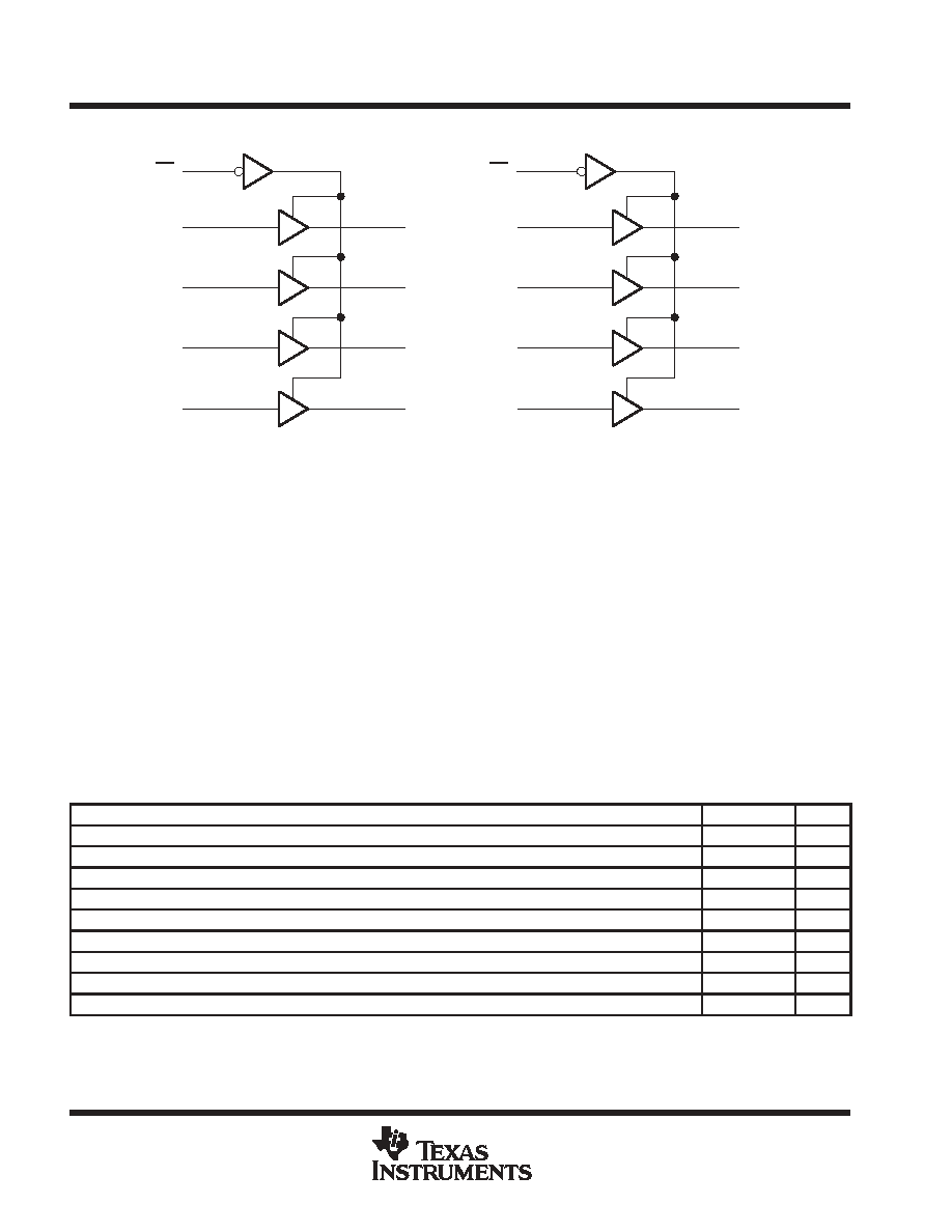
logic diagram (positive logic)
1
2
18
1Y1
1OE
1A1
4
16
1Y2
1A2
6
14
1Y3
1A3
8
12
1Y4
1A4
19
11
9
2Y1
2OE
2A1
13
7
2Y2
2A2
15
5
2Y3
2A3
17
3
2Y4
2A4
absolute maximum ratings over operating free-air temperature range (unless otherwise noted)
DC supply voltage range, V
CC
≠0.5 V to 6 V
. . . . . . . . . . . . . . . . . . . . . . . . . . . . . . . . . . . . . . . . . . . . . . . . . . . . . . .
DC input clamp current, I
IK
(V
I
< ≠0.5 V)
≠20 mA
. . . . . . . . . . . . . . . . . . . . . . . . . . . . . . . . . . . . . . . . . . . . . . . . . . .
DC output clamp current, I
OK
(V
O
< ≠0.5 V)
≠50 mA
. . . . . . . . . . . . . . . . . . . . . . . . . . . . . . . . . . . . . . . . . . . . . . . .
DC output sink current per output pin, I
OL
70
mA
. . . . . . . . . . . . . . . . . . . . . . . . . . . . . . . . . . . . . . . . . . . . . . . . . . .
DC output source current per output pin, I
OH
≠30
mA
. . . . . . . . . . . . . . . . . . . . . . . . . . . . . . . . . . . . . . . . . . . . . . .
Continuous current through V
CC
, I
CC
140
mA
. . . . . . . . . . . . . . . . . . . . . . . . . . . . . . . . . . . . . . . . . . . . . . . . . . . . . .
Continuous current through GND
528 mA
. . . . . . . . . . . . . . . . . . . . . . . . . . . . . . . . . . . . . . . . . . . . . . . . . . . . . . . . . .
Package thermal impedance,
JA
(see Note 1): E package
69
∞
C/W
. . . . . . . . . . . . . . . . . . . . . . . . . . . . . . . . . . .
M package
58
∞
C/W
. . . . . . . . . . . . . . . . . . . . . . . . . . . . . . . . . .
SM package
70
∞
C/W
. . . . . . . . . . . . . . . . . . . . . . . . . . . . . . . . .
Storage temperature range, T
stg
≠65
∞
C to 150
∞
C
. . . . . . . . . . . . . . . . . . . . . . . . . . . . . . . . . . . . . . . . . . . . . . . . . . .
Stresses beyond those listed under "absolute maximum ratings" may cause permanent damage to the device. These are stress ratings only, and
functional operation of the device at these or any other conditions beyond those indicated under "recommended operating conditions" is not
implied. Exposure to absolute-maximum-rated conditions for extended periods may affect device reliability.
NOTES:
1. The package thermal impedance is calculated in accordance with JESD 51-7.
recommended operating conditions (see Note 2)
MIN
MAX
UNIT
VCC
Supply voltage
4.75
5.25
V
VIH
High-level input voltage
2
V
VIL
Low-level input voltage
0.8
V
VI
Input voltage
0
VCC
V
VO
Output voltage
0
VCC
V
IOH
High-level output current
≠15
mA
IOL
Low-level output current
64
mA
t/
v
Input transition rise or fall rate (slew rate)
10
ns/V
TA
Operating free-air temperature
0
70
∞
C
NOTE 2: All unused inputs of the device must be held at VCC or GND to ensure proper device operation. Refer to the TI application report,
Implications of Slow or Floating CMOS Inputs, literature number SCBA004.
CD74FCT244, CD74FCT244AT
BiCMOS OCTAL BUFFERS/LINE DRIVERS
WITH 3-STATE OUTPUTS
SCBS722B ≠ JULY 2000 ≠ REVISED AUGUST 2003
3
POST OFFICE BOX 655303
∑
DALLAS, TEXAS 75265
electrical characteristics over recommended operating free-air temperature range (unless
otherwise noted)
PARAMETER
TEST CONDITIONS
VCC
TA = 25
∞
C
MIN
MAX
UNIT
PARAMETER
TEST CONDITIONS
VCC
MIN
MAX
MIN
MAX
UNIT
VIK
II = ≠18 mA
4.75 V
≠1.2
≠1.2
V
VOH
IOH = ≠15 mA
4.75 V
2.4
2.4
V
VOL
IOL = 64 mA
4.75 V
0.55
0.55
V
II
VI = VCC or GND
5.25 V
±
0.1
±
1
m
A
IOZ
VO = VCC or GND
5.25 V
±
0.5
±
10
m
A
IOS
VI = VCC or GND,
VO = 0
5.25 V
≠60
≠60
mA
ICC
VI = VCC or GND,
IO = 0
5.25 V
8
80
m
A
ICC
One input at 3.4 V,
Other inputs at VCC or GND
5.25 V
1.6
1.6
mA
Ci
VI = VCC or GND
10
10
pF
Co
VO = VCC or GND
15
15
pF
Not more than one output should be tested at a time, and the duration of the test should not exceed 100 ms.
This is the increase in supply current for each input at one of the specified TTL voltage levels, rather than 0 V or VCC.
switching characteristics over recommended operating free-air temperature range,
V
CC
= 5 V
±
0.25 V (unless otherwise noted) (see Figure 1)
PARAMETER
FROM
TO
CD74FCT244
CD74FCT244AT
UNIT
PARAMETER
FROM
(INPUT)
TO
(OUTPUT)
TA = 25
∞
C
MIN
MAX
TA = 25
∞
C
MIN
MAX
UNIT
(INPUT)
(OUTPUT)
TYP
MIN
MAX
TYP
MIN
MAX
tpd
A
Y
4.5
1.5
6.5
3.8
1.5
5.3
ns
ten
OE
Y
6
1.5
8
4.8
1.5
6.5
ns
tdis
OE
Y
5
1.5
7
4.5
1.5
5.8
ns
noise characteristics, V
CC
= 5 V, C
L
= 50 pF, T
A
= 25
∞
C
PARAMETER
MIN
TYP
MAX
UNIT
VOL(P)
Quiet output, maximum dynamic VOL
1
V
VOH(V)
Quiet output, minimum dynamic VOH
0.5
V
VIH(D)
High-level dynamic input voltage
2
V
VIL(D)
Low-level dynamic input voltage
0.8
V
operating characteristics, V
CC
= 5 V, T
A
= 25
∞
C
PARAMETER
TEST CONDITIONS
TYP
UNIT
Cpd
Power dissipation capacitance
No load,
f = 1 MHz
35
pF
CD74FCT244, CD74FCT244AT
BiCMOS OCTAL BUFFERS/LINE DRIVERS
WITH 3-STATE OUTPUTS
SCBS722B ≠ JULY 2000 ≠ REVISED AUGUST 2003
4
POST OFFICE BOX 655303
∑
DALLAS, TEXAS 75265
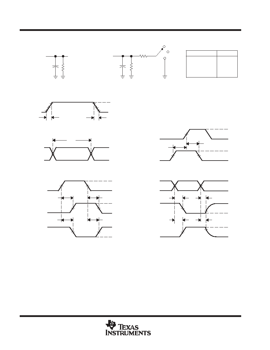
PARAMETER MEASUREMENT INFORMATION
3 V
3 V
0 V
0 V
th
tsu
VOLTAGE WAVEFORMS
SETUP AND HOLD TIMES
Data Input
tPLH
tPHL
tPHL
tPLH
VOH
VOH
VOL
VOL
3 V
0 V
1.5 V
1.5 V
Input
Out-of-Phase
Output
In-Phase
Output
Timing Input
VOLTAGE WAVEFORMS
PROPAGATION DELAY TIMES
INVERTING AND NONINVERTING OUTPUTS
Output
Control
Output
Waveform 1
(see Note B)
Output
Waveform 2
(see Note B)
VOL
VOH
tPZL
tPZH
tPLZ
tPHZ
3.5 V
0 V
1.5 V
VOL
+ 0.3 V
1.5 V
0 V
3 V
VOLTAGE WAVEFORMS
ENABLE AND DISABLE TIMES
LOW- AND HIGH-LEVEL ENABLING
tPLH/tPHL
tPLZ/tPZL
tPHZ/tPZH
Open Drain
Open
7 V
Open
7 V
TEST
S1
3 V
0 V
1.5 V
tw
VOLTAGE WAVEFORMS
PULSE DURATION
Input
NOTES: A. CL includes probe and jig capacitance.
B. Waveform 1 is for an output with internal conditions such that the output is low except when disabled by the output control.
Waveform 2 is for an output with internal conditions such that the output is high except when disabled by the output control.
C. All input pulses are supplied by generators having the following characteristics: PRR
1 MHz, ZO = 50
, tr and tf = 2.5 ns.
D. The outputs are measured one at a time with one input transition per measurement.
E. tPLZ and tPHZ are the same as tdis.
F. tPZL and tPZH are the same as ten.
G. tPHL and tPLH are the same as tpd.
From Output
Under Test
CL = 50 pF
(see Note A)
LOAD CIRCUIT FOR
3-STATE AND OPEN-DRAIN OUTPUTS
S1
7 V
500
GND
From Output
Under Test
CL = 50 pF
(see Note A)
Test
Point
LOAD CIRCUIT FOR
TOTEM-POLE OUTPUTS
Open
VOH ≠
0.3 V
1.5 V
1.5 V
1.5 V
1.5 V
1.5 V
1.5 V
1.5 V
1.5 V
500
500
1.5 V
1.5 V
VOLTAGE WAVEFORM
INPUT RISE AND FALL TIMES
1.5 V
1.5 V
10%
10%
90%
90%
3 V
0 V
tr
tf
Figure 1. Load Circuit and Voltage Waveforms
MECHANICAL
MPDI002C ≠ JANUARY 1995 ≠ REVISED DECEMBER 20002
1
POST OFFICE BOX 655303
∑
DALLAS, TEXAS 75265
N (R-PDIP-T**)
PLASTIC DUAL-IN-LINE PACKAGE
BB
AC
AD
0.325 (8,26)
0.300 (7,62)
0.010 (0,25) NOM
Gauge Plane
0.015 (0,38)
0.430 (10,92) MAX
20
1.060
(26,92)
0.940
(23,88)
18
0.920
0.850
14
0.775
0.745
(19,69)
(18,92)
16
0.775
(19,69)
(18,92)
0.745
A MIN
DIM
A MAX
PINS **
(23,37)
(21,59)
Seating Plane
14/18 PIN ONLY
20 pin vendor option
4040049/E 12/2002
9
8
0.070 (1,78)
A
0.045 (1,14)
0.020 (0,51) MIN
16
1
0.015 (0,38)
0.021 (0,53)
0.200 (5,08) MAX
0.125 (3,18) MIN
0.240 (6,10)
0.260 (6,60)
M
0.010 (0,25)
0.100 (2,54)
16 PINS SHOWN
MS-100
VARIATION
AA
C
D
D
D
0.030 (0,76)
0.045 (1,14)
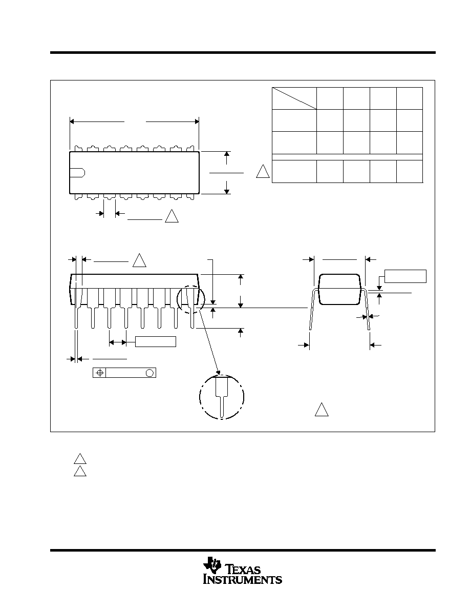
NOTES: A. All linear dimensions are in inches (millimeters).
B. This drawing is subject to change without notice.
C. Falls within JEDEC MS-001, except 18 and 20 pin minimum body lrngth (Dim A).
D. The 20 pin end lead shoulder width is a vendor option, either half or full width.