1
Data sheet acquired from Harris Semiconductor
SCHS254
Features
∑ Buffered Inputs
∑ Typical Propagation Delay: 5.3ns at V
CC
= 5V,
T
A
= 25
o
C, C
L
= 50pF
∑ SCR Latchup Resistant BiCMOS Process and
Circuit Design
∑ Speed of Bipolar FASTTM/AS/S
∑ 48mA Output Sink Current
∑ Output Voltage Swing Limited to 3.7V at V
CC
= 5V
∑ Controlled Output Edge Rates
∑ Input/Output Isolation to V
CC
∑ BiCMOS Technology with Low Quiescent Power
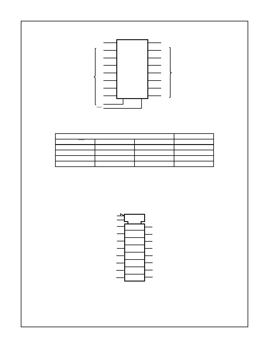
Pinout
Ordering Information
PART NUMBER
TEMP.
RANGE (
o
C)
PACKAGE
PKG.
NO.
CD74FCT273E
0 to 70
20 Ld PDIP
E20.3
CD74FCT273M
0 to 70
20 Ld SOIC
M20.3
NOTE: When ordering the suffix M package, use the entire part
number. Add the suffix 96 to obtain the variant in the tape and reel.
CD74FCT273
(PDIP, SOIC)
TOP VIEW
11
12
13
14
15
16
17
18
20
19
10
9
8
7
6
5
4
3
2
1
MR
Q0
D0
D1
Q1
Q2
D3
D2
Q3
GND
V
CC
D7
D6
Q6
Q5
D5
D4
Q4
CP
Q7
January 1997
CAUTION: These devices are sensitive to electrostatic discharge. Users should follow proper IC Handling Procedures.
FASTTM is a trademark of Fairchild Semiconductor.
Copyright
©
Harris Corporation 1997
CD74FCT273
BiCMOS FCT Interface Logic,
Octal D Flip-Flop with Reset
NOT RECOMMENDED
FOR NEW DESIGNS
Use CMOS T
echnology
File Number
2303.2
3
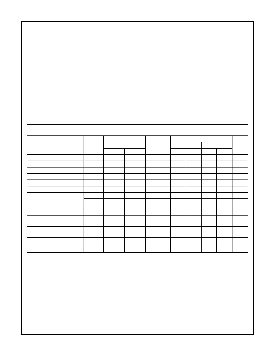
Absolute Maximum Ratings
Thermal Information
DC Supply Voltage (V
CC
) . . . . . . . . . . . . . . . . . . . . . . . . -0.5V to 6V
DC Input Diode Current, I
IK
(For V
I
< -0.5V) . . . . . . . . . . . . . -20mA
DC Output Diode Current, I
OK
(for V
O
< -0.5V) . . . . . . . . . . . -50mA
DC Output Sink Current per Output Pin, IO . . . . . . . . . . . . . . . 70mA
DC Output Source Current per Output Pin, IO . . . . . . . . . . . . -30mA
DC V
CC
Current (I
CC
) . . . . . . . . . . . . . . . . . . . . . . . . . . . . . . 140mA
DC Ground Current (I
GND
). . . . . . . . . . . . . . . . . . . . . . . . . . . 400mA
Operating Conditions
Operating Temperature Range (T
A
) . . . . . . . . . . . . . . . .0
o
C to 70
o
C
Supply Voltage Range, V
CC
. . . . . . . . . . . . . . . . . . . .4.75V to 5.25V
DC Input Voltage, V
I
. . . . . . . . . . . . . . . . . . . . . . . . . . . . . . 0 to V
CC
DC Output Voltage, V
O
. . . . . . . . . . . . . . . . . . . . . . . . . . . 0 to
V
CC
Input Rise and Fall Slew Rate, dt/dv. . . . . . . . . . . . . . . . 0 to 10ns/V
Thermal Resistance (Typical, Note 2)
JA
(
o
C/W)
PDIP Package . . . . . . . . . . . . . . . . . . . . . . . . . . . . . . . . . 135
SOIC Package . . . . . . . . . . . . . . . . . . . . . . . . . . . . . . . . . 125
Maximum Junction Temperature . . . . . . . . . . . . . . . . . . . . . . . 150
o
C
Maximum Storage Temperature Range . . . . . . . . . .-65
o
C to 150
o
C
Maximum Lead Temperature (Soldering 10s) . . . . . . . . . . . . . 300
o
C
(SOIC-Lead Tips Only)
CAUTION: Stresses above those listed in "Absolute Maximum Ratings" may cause permanent damage to the device. This is a stress only rating and operation
of the device at these or any other conditions above those indicated in the operational sections of this specification is not implied.
NOTE:
2.
JA
is measured with the component mounted on an evaluation PC board in free air.
Electrical Specifications
Commercial Temperature Range 0
o
C to 70
o
C, V
CC
Max = 5.25V, V
CC
Min = 4.75V (Note 5)
PARAMETER
SYMBOL
TEST CONDITIONS
V
CC
(V)
AMBIENT TEMPERATURE (T
A
)
UNITS
25
o
C
0
o
C TO 70
o
C
V
I
(V)
I
O
(mA)
MIN
MAX
MIN
MAX
High Level Input Voltage
V
IH
4.75 to 5.25
2
-
2
-
V
Low Level Input Voltage
V
IL
4.75 to 5.25
-
0.8
-
0.8
V
High Level Output Voltage
V
OH
V
IH
or V
IL
-15
Min
2.4
-
2.4
-
V
Low Level Output Voltage
V
OL
V
IH
or V
IL
48
Min
-
0.55
-
0.55
V
High Level Input Current
I
IH
V
CC
Max
-
0.1
-
1
µ
A
Low Level Input Current
I
IL
GND
Max
-
-0.1
-
-1
µ
A
Three State Leakage Current
I
OZH
V
CC
Max
-
0.5
-
10
µ
A
I
OZL
GND
Max
-
-0.5
-
-10
µ
A
Input Clamp Voltage
V
IK
V
CC
or
GND
-18
Min
-
-1.2
-
-1.2
V
Short Circuit Output Current
(Note 3)
I
OS
V
O
= 0 V
CC
or GND
Max
-60
-
-60
-
mA
Quiescent Supply Current,
MSI
I
CC
V
CC
or
GND
0
Max
-
8
-
80
µ
A
Additional Quiescent Supply
Current per Input Pin
TTL Inputs High, 1 Unit Load
I
CC
3.4V
(Note 4)
Max
-
1.6
-
1.6
mA
NOTES:
3. Not more than one output should be shorted at one time. Test duration should not exceed 100ms.
4. Inputs that are not measured are at V
CC
or GND.
5. FCT Input Loading: All inputs are 1 unit load. Unit load is
I
CC
limit specified in Static Characteristics Chart, e.g., 1.6mA Max. at 70
o
C.
CD74FCT273
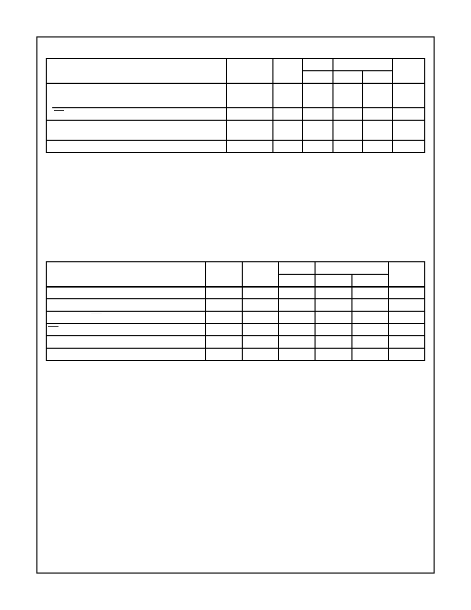
4
Switching Specifications Over Operating Range
FCT Series t
r
, t
f
= 2.5ns, C
L
= 50pF, R
L
(Figure 4) (Note 6)
PARAMETER
SYMBOL
V
CC
(V)
25
o
C
0
o
C TO 70
o
C
UNITS
TYP
MIN
MAX
Propagation Delays
CP to Qn
t
PLH
, t
PHL
5
7
2
13
ns
MR to Qn
t
PLH
, t
PHL
5
8
2
13
ns
Power Dissipation Capacitance
C
PD
(Note 7)
-
36
-
-
pF
Input Capacitance
C
I
-
-
-
10
pF
NOTES:
6. 5V: Min is at 5.25V for 0
o
C to 70
o
C, Max is at 4.75V for 0
o
C to 70
o
C, Typ is at 5V.
7. C
PD
, measured per flip-flop, is used to determine the dynamic power consumption.
P
D
(per package) = V
CC
I
CC
+
(V
CC
2
f
I
C
PD
+ V
O
2
f
O
C
L
+ V
CC
I
CC
D) where:
V
CC
= supply voltage
I
CC
= flow through current x unit load
C
L
= output load capacitance
D = duty cycle of input high
f
O
= output frequency
f
I
= input frequency
Prerequisite for Switching
(Note 8)
PARAMETER
SYMBOL
V
CC
(V)
25
o
C
0
o
C TO 70
o
C
UNITS
TYP
MIN
MAX
Data to CP Setup Time
t
SU
5
-
3
-
ns
Hold Time
t
H
5
-
2
-
ns
Removal Time, MR to CP
t
REM
5
-
4
-
ns
MR Pulse Width
t
W
5
-
7
-
ns
CP Pulse Width
t
W
5
-
7
-
ns
CP Frequency
f
MAX
5
-
70
-
MHz
NOTE:
8. 5V: Minimum is at 4.75V for 0
o
C to 70
o
C, Typical is at 5V.
CD74FCT273
5
CD74FCT273
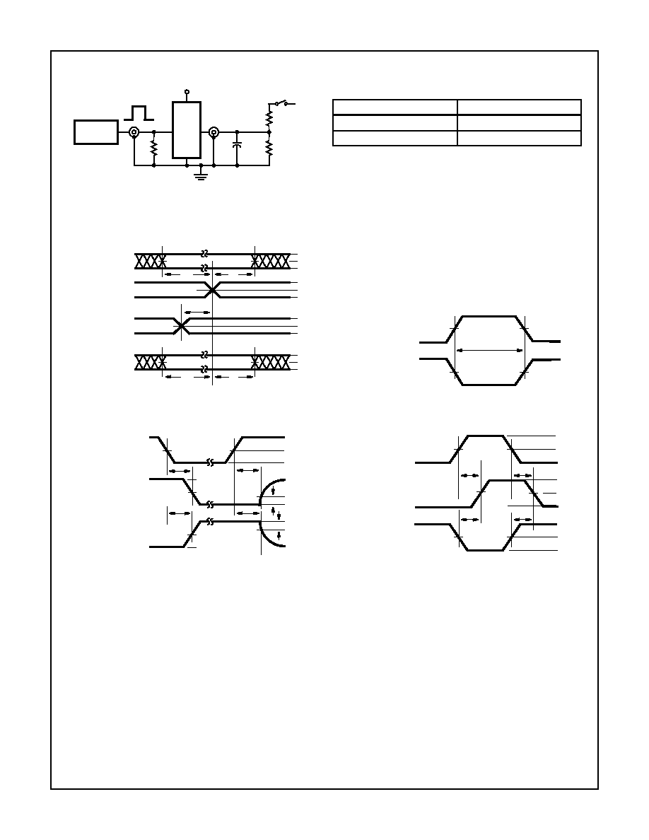
Test Circuits and Waveforms
NOTE:
9. Pulse Generator for All Pulses: Rate
1.0MHz; Z
OUT
50
;
t
f
, t
r
2.5ns.
FIGURE 1. TEST CIRCUIT
FIGURE 2. SETUP, HOLD, AND RELEASE TIMING
FIGURE 3. PULSE WIDTH
FIGURE 4. ENABLE AND DISABLE TIMING
FIGURE 5. PROPAGATION DELAY
3V
0
DUT
PULSE Z
O
GEN
7V
500
50pF
500
V
CC
R
T
R
T
= Z
O
V
0
C
L
R
L
R
L
V
I
t
r
, t
f
= 2.5ns
(NOTE 9)
SWITCH POSITION
TEST
SWITCH
t
PLZ
, t
PZL
, Open Drain
Closed
t
PHZ
, t
PZH
, t
PLH
, t
PHL
Open
DEFINITIONS:
C
L
= Load capacitance, includes jig and probe
capacitance.
R
T
= Termination resistance, should be equal to Z
OUT
of
the Pulse Generator.
V
IN
= 0V to 3V.
Input: t
r
= t
f
= 2.5ns (10% to 90%), unless otherwise specified
ASYNCHRONOUS CONTROL
t
H
t
SH
3V
1.5V
0V
3V
1.5V
0V
3V
1.5V
0V
3V
1.5V
0V
t
H
t
SH
PRESET CLEAR
CLOCK ENABLE
ETC.
SYNCHRONOUS CONTROL
t
REM
DATA
INPUT
TIMING
INPUT
t
W
LOW-HIGH-LOW
PULSE
HIGH-LOW-HIGH
PULSE
1.5V
1.5V
3V
1.5V
0V
CONTROL INPUT
OUTPUT
NORMALLY LOW
OUTPUT
NORMALLY HIGH
SWITCH
OPEN
t
PZL
3.5V
1.5V
1.5V
0V
t
PLZ
t
PHZ
t
PZH
0V
3.5V
0.3V
0.3V
V
OL
V
OH
SWITCH
CLOSED
ENABLE
DISABLE
1.5V
3V
0V
1.5V
3V
0V
t
PLH
SAME PHASE
INPUT TRANSITION
t
PHL
t
PLH
t
PHL
OPPOSITE PHASE
INPUT TRANSITION
OUTPUT
1.5V
V
OH
V
OL