8-1
Data sheet acquired from Harris Semiconductor
SCHS258
Features
∑ Buffered Inputs
∑ Typical Propagation Delay: 6.4ns at V
CC
= 5V,
T
A
= 25
o
C, C
L
= 50pF
∑ Noninverting
∑ Family Features
- SCR Latchup Resistant BiCMOS Process and
Circuit Design
- Speed of Bipolar FASTTM/AS/S
- 64mA Output Sink Current
- Output Voltage Swing Limited to 3.7V at V
CC
= 5V
- Controlled Output Edge Rates
- Input/Output Isolation to V
CC
- BiCMOS Technology with Low Quiescent Power
Pinout
Ordering Information
PART NUMBER
TEMP.
RANGE (
o
C)
PACKAGE
PKG.
NO.
CD74FCT543EN
0 to 70
24 Ld PDIP
E24.3
CD74FCT543M
0 to 70
24 Ld SOIC
M24.3
CD74FCT543SM
0 to 70
24 Ld SSOP
M24.209
NOTE: When ordering the suffix M and SM packages, use the entire
part number. Add the suffix 96 to obtain the variant in the tape and reel.
CD74FCT543
(PDIP, SOIC, SSOP)
TOP VIEW
1
2
3
4
5
6
7
8
9
10
11
12
LEBA
OEBA
A0
GND
16
17
18
19
20
21
22
23
24
15
14
13
VCC
B0
B2
B3
B5
B7
LEAB
OEAB
CEBA
B4
B6
A1
A2
A3
A5
A6
A7
CEAB
A4
B1
January 1997
CAUTION: These devices are sensitive to electrostatic discharge. Users should follow proper IC Handling Procedures.
FASTTM is a trademark of Fairchild Semiconductor.
Copyright
©
Harris Corporation 1997
CD74FCT543
BiCMOS FCT Interface Logic,
Octal Register/Transceiver, Three-State
NOT RECOMMENDED
FOR NEW DESIGNS
Use CMOS T
echnology
File Number
2399.2
8-2
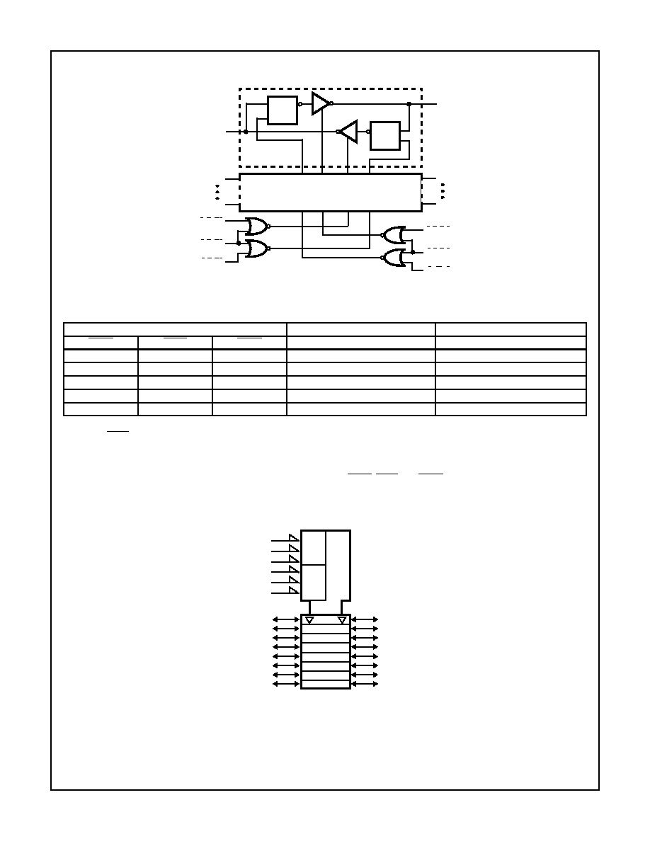
Functional Diagram
IEC Logic Symbol
TRUTH TABLE For A to B (Symmetric with B to A)
INPUTS
LATCH STATUS
OUTPUT BUFFERS
CEAB
LEAB
OEAB
A TO B
B0 THRU B7
H
X
X
Storing
High Z
X
H
-
Storing
-
X
-
H
-
High Z
L
L
L
Transparent
Current A Inputs
L
H
L
Storing
Previous A Inputs (Note 1)
NOTE:
1. Before LEAB LOW to HIGH Transition
H = HIGH Voltage Level
L = LOW Voltage Level
X = Immaterial
A to B data flow shown; B to A flow control is the same, except using CEBA, LEBA, and OEBA.
D
LE
Q
DETAIL A
DETAIL A x 7
Q
D
LE
B0
B1
B7
OEAB
CEAB
LEAB
A0
A1
A7
OEBA
CEBA
LEBA
CD74FCT543
22
21
20
19
18
17
16
EN1
15
EN2
3
4
5
6
7
8
9
10
1
1
11
14
13
23
1
2
1
2
CD74FCT543
8-3
Absolute Maximum Ratings
Thermal Information
DC Supply Voltage (V
CC
) . . . . . . . . . . . . . . . . . . . . . . . . -0.5V to 6V
DC Input Diode Current, I
IK
(For V
I
< -0.5V) . . . . . . . . . . . . . -20mA
DC Output Diode Current, I
OK
(for V
O
< -0.5V) . . . . . . . . . . . -50mA
DC Output Sink Current per Output Pin, IO . . . . . . . . . . . . . . . 70mA
DC Output Source Current per Output Pin, IO . . . . . . . . . . . . -30mA
DC V
CC
Current (I
CC
) . . . . . . . . . . . . . . . . . . . . . . . . . . . . . . 140mA
DC Ground Current (I
GND
). . . . . . . . . . . . . . . . . . . . . . . . . . . 528mA
Operating Conditions
Operating Temperature Range (T
A
) . . . . . . . . . . . . . . . .0
o
C to 70
o
C
Supply Voltage Range, V
CC
. . . . . . . . . . . . . . . . . . . .4.75V to 5.25V
DC Input Voltage, V
I
. . . . . . . . . . . . . . . . . . . . . . . . . . . . . . 0 to V
CC
DC Output Voltage, V
O
. . . . . . . . . . . . . . . . . . . . . . . . . . . 0 to
V
CC
Input Rise and Fall Slew Rate, dt/dv. . . . . . . . . . . . . . . . 0 to 10ns/V
Thermal Resistance (Typical, Note 2)
JA
(
o
C/W)
PDIP Package . . . . . . . . . . . . . . . . . . . . . . . . . . . . . . . . . . 75
SOIC Package . . . . . . . . . . . . . . . . . . . . . . . . . . . . . . . . . . 75
SSOP Package . . . . . . . . . . . . . . . . . . . . . . . . . . . . . . . . 125
Maximum Junction Temperature . . . . . . . . . . . . . . . . . . . . . . . 150
o
C
Maximum Storage Temperature Range . . . . . . . . . .-65
o
C to 150
o
C
Maximum Lead Temperature (Soldering 10s) . . . . . . . . . . . . . 300
o
C
(SOIC and SSOP-Lead Tips Only)
CAUTION: Stresses above those listed in "Absolute Maximum Ratings" may cause permanent damage to the device. This is a stress only rating and operation
of the device at these or any other conditions above those indicated in the operational sections of this specification is not implied.
NOTE:
2.
JA
is measured with the component mounted on an evaluation PC board in free air.
Electrical Specifications
Commercial Temperature Range 0
o
C to 70
o
C, V
CC
Max = 5.25V, V
CC
Min = 4.75V
PARAMETER
SYMBOL
TEST CONDITIONS
V
CC
(V)
AMBIENT TEMPERATURE (T
A
)
UNITS
25
o
C
0
o
C TO 70
o
C
V
I
(V)
I
O
(mA)
MIN
MAX
MIN
MAX
High Level Input Voltage
V
IH
4.75 to
5.25
2
-
2
-
V
Low Level Input Voltage
V
IL
4.75 to
5.25
-
0.8
-
0.8
V
High Level Output Voltage
V
OH
V
IH
or V
IL
-15
Min
2.4
-
2.4
-
V
Low Level Output Voltage
V
OL
V
IH
or V
IL
64
Min
-
0.55
-
0.55
V
High Level Input Current
I
IH
V
CC
Max
-
0.1
-
1
µ
A
Low Level Input Current
I
IL
GND
Max
-
-0.1
-
-1
µ
A
Three-State Leakage Current
I
OZH
V
CC
Max
-
0.5
-
10
µ
A
I
OZL
GND
Max
-
-0.5
-
-10
µ
A
Input Clamp Voltage
V
IK
V
CC
or
GND
-18
Min
-
-1.2
-
-1.2
V
Short Circuit Output Current
(Note 3)
I
OS
V
O
= 0
V
CC
or
GND
Max
-60
-
-60
-
mA
Quiescent Supply Current,
MSI
I
CC
V
CC
or
GND
0
Max
-
8
-
80
µ
A
Additional Quiescent Supply
Current per Input Pin
TTL Inputs High, 1 Unit Load
I
CC
3.4V
(Note 4)
Max
-
1.6
-
1.6
mA
NOTES:
3. Not more than one output should be shorted at one time. Test duration should not exceed 100ms.
4. Inputs that are not measured are at V
CC
or GND.
5. FCT Input Loading: All inputs are 1 unit load. Unit load is
I
CC
limit specified in Electrical Specifications table, e.g., 1.6mA Max. at 70
o
C.
CD74FCT543

8-4
Switching Specifications Over Operating Range
FCT Series t
r
, t
f
= 2.5ns, C
L
= 50pF, R
L
(Figure 4)
PARAMETER
SYMBOL
V
CC
(V)
25
o
C
0
o
C TO 70
o
C
UNITS
TYP
MIN
TYP
MAX
Propagation Delays
An
Bn
t
PLH
, t
PHL
5
6.4
2.5
-
8.5
ns
LEBA to An or LEAB to Bn
t
PLH
, t
PHL
5
9.4
2.5
-
12.5
ns
CEBA or CEAB to An or Bn
t
PLZ
, t
PHZ
5
6.8
2
-
9
ns
t
PZL
, t
PZH
5
9
2
-
12
ns
Power Dissipation Capacitance
C
PD
(Note 6)
-
49
-
49
-
pF
Minimum (Valley) V
OHV
During Switching of
Other Outputs (Output Under Test Not Switching)
V
OHV
5
0.5
-
-
-
V
Maximum (Peak) V
OLP
During Switching of
Other Outputs (Output Under Test Not Switching)
V
OLP
5
1
-
-
-
V
Input Capacitance
C
I
-
-
-
-
10
pF
Input/Output Capacitance
C
I/O
-
-
-
-
15
pF
NOTE:
6. C
PD
, measured per flip-flop, is used to determine the dynamic power consumption.
P
D
(per package) = V
CC
I
CC
+
(V
CC
2
f
I
C
PD
+ V
O
2
f
O
C
L
+ V
CC
I
CC
D) where:
V
CC
= supply voltage
I
CC
= flow through current x unit load
C
L
= output load capacitance
D = duty cycle of input high
f
O
= output frequency
f
I
= input frequency
Prerequisite for Switching
PARAMETER
SYMBOL
V
CC
(V)
25
o
C
0
o
C TO 70
o
C
UNITS
TYP
MIN
MAX
Data to Latch Enable Setup Time
t
SU
5
(Note 7)
-
3
-
ns
Data to Latch Enable Hold Time
t
H
5
-
2
-
ns
Latch Enable Pulse Width
t
W
5
-
9
-
ns
NOTE:
7. 5V: Minimum is at 4.75V for 0
o
C to 70
o
C, Typical is at 5V.
CD74FCT543

8-5
Test Circuits and Waveforms
NOTE:
8. Pulse Generator for All Pulses: Rate
1.0MHz; Z
OUT
50
;
t
f
, t
r
2.5ns.
FIGURE 1. TEST CIRCUIT
FIGURE 2. SETUP, HOLD, AND RELEASE TIMING
FIGURE 3. PULSE WIDTH
FIGURE 4. ENABLE AND DISABLE TIMING
FIGURE 5. PROPAGATION DELAY
NOTES:
9. V
OLP
is measured with respect to a ground reference near the output under test. V
OHV
is measured with respect to V
OH
.
10. Input pulses have the following characteristics:
P
RR
1MHz, t
r
= 2.5ns, t
f
= 2.5ns, skew 1ns.
11. R.F. fixture with 700MHz design rules required. IC should be soldered into test board and bypassed with 0.1
µ
F capacitor. Scope and
probes require 700MHz bandwidth.
FIGURE 6. SIMULTANEOUS SWITCHING TRANSIENT WAVEFORMS
3V
0
DUT
PULSE Z
O
GEN
7V
500
50pF
500
V
CC
R
T
R
T
= Z
O
V
0
C
L
R
L
R
L
V
I
t
r
, t
f
= 2.5ns
(NOTE 8)
SWITCH POSITION
TEST
SWITCH
t
PLZ
, t
PZL
, Open Drain
Closed
t
PHZ
, t
PZH
, t
PLH
, t
PHL
Open
DEFINITIONS:
C
L
= Load capacitance, includes jig and probe
capacitance.
R
T
= Termination resistance, should be equal to Z
OUT
of
the Pulse Generator.
V
IN
= 0V to 3V.
Input: t
r
= t
f
= 2.5ns (10% to 90%), unless otherwise specified
ASYNCHRONOUS CONTROL
t
H
t
SH
3V
1.5V
0V
3V
1.5V
0V
3V
1.5V
0V
3V
1.5V
0V
t
H
t
SH
PRESET CLEAR
CLOCK ENABLE
ETC.
SYNCHRONOUS CONTROL
t
REM
DATA
INPUT
TIMING
INPUT
t
W
LOW-HIGH-LOW
PULSE
HIGH-LOW-HIGH
PULSE
1.5V
1.5V
3V
1.5V
0V
CONTROL INPUT
OUTPUT
NORMALLY LOW
OUTPUT
NORMALLY HIGH
SWITCH
OPEN
t
PZL
3.5V
1.5V
1.5V
0V
t
PLZ
t
PHZ
t
PZH
0V
3.5V
0.3V
0.3V
V
OL
V
OH
SWITCH
CLOSED
ENABLE
DISABLE
1.5V
3V
0V
1.5V
3V
0V
t
PLH
SAME PHASE
INPUT TRANSITION
t
PHL
t
PLH
t
PHL
OPPOSITE PHASE
INPUT TRANSITION
OUTPUT
1.5V
V
OH
V
OL
OTHER
OUTPUTS
OUTPUT
UNDER
TEST
V
OH
V
OL
V
OH
V
OHV
V
OLP
V
OL
CD74FCT543