1
Data sheet acquired from Harris Semiconductor
SCHS163F
Features
∑ Synchronous Counting and Asynchronous
Loading
∑ Two Outputs for N-Bit Cascading
∑ Look-Ahead Carry for High-Speed Counting
∑ Fanout (Over Temperature Range)
- Standard Outputs . . . . . . . . . . . . . . . 10 LSTTL Loads
- Bus Driver Outputs . . . . . . . . . . . . . 15 LSTTL Loads
∑ Wide Operating Temperature Range . . . -55
o
C to 125
o
C
∑ Balanced Propagation Delay and Transition Times
∑ Significant Power Reduction Compared to LSTTL
Logic ICs
∑ HC Types
- 2V to 6V Operation
- High Noise Immunity: N
IL
= 30%, N
IH
= 30% of V
CC
at V
CC
= 5V
∑ HCT Types
- 4.5V to 5.5V Operation
- Direct LSTTL Input Logic Compatibility,
V
IL
= 0.8V (Max), V
IH
= 2V (Min)
- CMOS Input Compatibility, I
l
1
µ
A at V
OL
, V
OH
Description
The 'HC192, 'HC193 and 'HCT193 are asynchronously
presettable BCD Decade and Binary Up/Down synchronous
counters, respectively.
Pinout
CD54HC192, CD54HC193, CD54HCT193 (CERDIP)
CD74HC192 (PDIP, SOP, TSSOP)
CD74HC193 (PDIP, SOIC)
CD74HCT193 (PDIP)
TOP VIEW
Presetting the counter to the number on the preset data inputs
(P0-P3) is accomplished by a LOW asynchronous parallel
load input (PL). The counter is incremented on the low-to-high
transition of the Clock-Up input (and a high level on the Clock-
Down input) and decremented on the low to high transition of
the Clock-Down input (and a high level on the Clock-up input).
A high level on the MR input overrides any other input to clear
the counter to its zero state. The Terminal Count up (carry)
goes low half a clock period before the zero count is reached
and returns to a high level at the zero count. The Terminal
Count Down (borrow) in the count down mode likewise goes
low half a clock period before the maximum count (9 in the
192 and 15 in the 193) and returns to high at the maximum
count. Cascading is effected by connecting the carry and
borrow outputs of a less significant counter to the Clock-Up
and Clock-Down inputs, respectively, of the next most
significant counter.
If a decade counter is preset to an illegal state or assumes an
illegal state when power is applied, it will return to the normal
sequence in one count as shown in state diagram.
14
15
16
9
13
12
11
10
1
2
3
4
5
7
6
8
P1
Q1
Q0
CPD
CPU
Q2
GND
Q3
V
CC
MR
TCD
TCU
PL
P2
P3
P0
Ordering Information
PART NUMBER
TEMP. RANGE
(
o
C)
PACKAGE
CD54HC192F3A
-55 to 125
16 Ld CERDIP
CD54HC193F3A
-55 to 125
16 Ld CERDIP
CD54HCT193F3A
-55 to 125
16 Ld CERDIP
CD74HC192E
-55 to 125
16 Ld PDIP
CD74HC192NSR
-55 to 125
16 Ld SOP
CD74HC192PW
-55 to 125
16 Ld TSSOP
CD74HC192PWR
-55 to 125
16 Ld TSSOP
CD74HC192PWT
-55 to 125
16 Ld TSSOP
CD74HC193E
-55 to 125
16 Ld PDIP
CD74HC193M
-55 to 125
16 Ld SOIC
CD74HC193MT
-55 to 125
16 Ld SOIC
CD74HC193M96
-55 to 125
16 Ld SOIC
CD74HCT193E
-55 to 125
16 Ld PDIP
NOTE: When ordering, use the entire part number. The suffixes 96
and R denote tape and reel. The suffix T denotes a small-quantity
reel of 250.
September 1997 - Revised October 2003
CAUTION: These devices are sensitive to electrostatic discharge. Users should follow proper IC Handling Procedures.
Copyright
©
2003, Texas Instruments Incorporated
CD54/74HC192,
CD54/74HC193, CD54/74HCT193
High-Speed CMOS Logic
Presettable Synchronous 4-Bit Up/Down Counters
[ /Title
(CD74
HC192
,
CD74
HC193
,
CD74
HCT19
3)
/Sub-
ject
(High
Speed
CMOS
Logic
Preset-
2
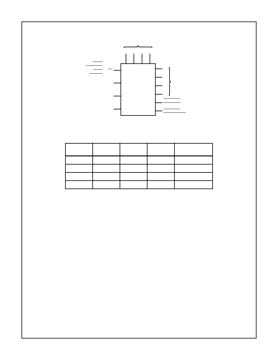
Functional Diagram
TRUTH TABLE
CLOCK UP
CLOCK
DOWN
RESET
PARALLEL
LOAD
FUNCTION
H
L
H
Count Up
H
L
H
Count Down
X
X
H
X
Reset
X
X
L
L
Load Preset Inputs
H = High Voltage Level, L = Low Voltage Level, X = Don't Care,
= Transition from Low to
High Level
ASYN.
MASTER
CLOCK UP
11
14
5
4
15
1
10
9
3
6
7
12
13
Q
0
Q
1
Q
2
Q
3
TERMINAL
P0
P1
P2
P3
LOAD
CLOCK DOWN
2
TERMINAL
COUNT UP
BCD (192)
BINARY (193)
OUTPUTS
BCD/BINARY
PRESET
ENABLE
PARALLEL
PL
RESET
COUNT DOWN
CD54/74HC192, CD54/74HC193, CD54/74HCT193
3
Absolute Maximum Ratings
Thermal Information
DC Supply Voltage, V
CC
. . . . . . . . . . . . . . . . . . . . . . . . -0.5V to 7V
DC Input Diode Current, I
IK
For V
I
< -0.5V or V
I
> V
CC
+ 0.5V
. . . . . . . . . . . . . . . . . . . . . .±
20mA
DC Output Diode Current, I
OK
For V
O
< -0.5V or V
O
> V
CC
+ 0.5V
. . . . . . . . . . . . . . . . . . . .±
20mA
DC Output Source or Sink Current per Output Pin, I
O
For V
O
> -0.5V or V
O
< V
CC
+ 0.5V
. . . . . . . . . . . . . . . . . . . .±
25mA
DC V
CC
or Ground Current, I
CC or
I
GND
. . . . . . . . . . . . . . . . . .±
50mA
Operating Conditions
Temperature Range (T
A
) . . . . . . . . . . . . . . . . . . . . . -55
o
C to 125
o
C
Supply Voltage Range, V
CC
HC Types . . . . . . . . . . . . . . . . . . . . . . . . . . . . . . . . . . . . .2V to 6V
HCT Types . . . . . . . . . . . . . . . . . . . . . . . . . . . . . . . . .4.5V to 5.5V
DC Input or Output Voltage, V
I
, V
O
. . . . . . . . . . . . . . . . . 0V to V
CC
Input Rise and Fall Time
2V . . . . . . . . . . . . . . . . . . . . . . . . . . . . . . . . . . . . . . 1000ns (Max)
4.5V. . . . . . . . . . . . . . . . . . . . . . . . . . . . . . . . . . . . . . 500ns (Max)
6V . . . . . . . . . . . . . . . . . . . . . . . . . . . . . . . . . . . . . . . 400ns (Max)
Package Thermal Impedance,
JA
(see Note 1):
E (PDIP) Package . . . . . . . . . . . . . . . . . . . . . . . . . . . . . . . 67
o
C/W
M (SOIC) Package. . . . . . . . . . . . . . . . . . . . . . . . . . . . . . . 73
o
C/W
NS (SOP) Package . . . . . . . . . . . . . . . . . . . . . . . . . . . . . 64
o
C/W
PW (TSSOP) Package . . . . . . . . . . . . . . . . . . . . . . . . . 108
o
C/W
Maximum Junction Temperature . . . . . . . . . . . . . . . . . . . . . . . 150
o
C
Maximum Storage Temperature Range . . . . . . . . . .-65
o
C to 150
o
C
Maximum Lead Temperature (Soldering 10s) . . . . . . . . . . . . . 300
o
C
(SOIC - Lead Tips Only)
CAUTION: Stresses above those listed in "Absolute Maximum Ratings" may cause permanent damage to the device. This is a stress only rating and operation
of the device at these or any other conditions above those indicated in the operational sections of this specification is not implied.
NOTE:
1. The package thermal impedance is calculated in accordance with JESD 51-7.
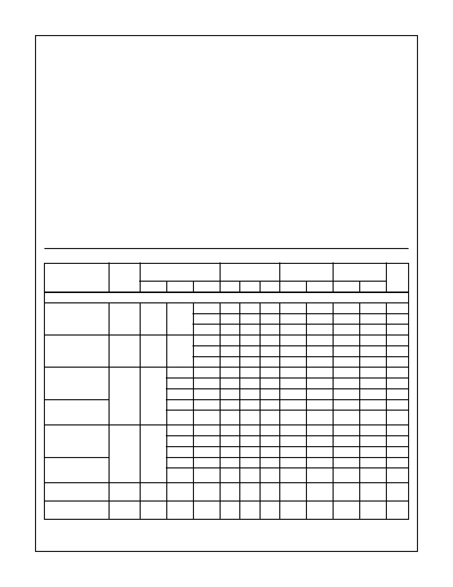
DC Electrical Specifications
PARAMETER
SYMBOL
TEST
CONDITIONS
25
o
C
-40
o
C TO 85
o
C
-55
o
C TO 125
o
C
UNITS
V
I
(V)
I
O
(mA)
V
CC
(V)
MIN
TYP
MAX
MIN
MAX
MIN
MAX
HC TYPES
High Level Input
Voltage
V
IH
-
-
2
1.5
-
-
1.5
-
1.5
-
V
4.5
3.15
-
-
3.15
-
3.15
-
V
6
4.2
-
-
4.2
-
4.2
-
V
Low Level Input
Voltage
V
IL
-
-
2
-
-
0.5
-
0.5
-
0.5
V
4.5
-
-
1.35
-
1.35
-
1.35
V
6
-
-
1.8
-
1.8
-
1.8
V
High Level Output
Voltage
CMOS Loads
V
OH
V
IH
or
V
IL
-0.02
2
1.9
-
-
1.9
-
1.9
-
V
-0.02
4.5
4.4
-
-
4.4
-
4.4
-
V
-0.02
6
5.9
-
-
5.9
-
5.9
-
V
High Level Output
Voltage
TTL Loads
-4
4.5
3.98
-
-
3.84
-
3.7
-
V
-5.2
6
5.48
-
-
5.34
-
5.2
-
V
Low Level Output
Voltage
CMOS Loads
V
OL
V
IH
or
V
IL
0.02
2
-
-
0.1
-
0.1
-
0.1
V
0.02
4.5
-
-
0.1
-
0.1
-
0.1
V
0.02
6
-
-
0.1
-
0.1
-
0.1
V
Low Level Output
Voltage
TTL Loads
4
4.5
-
-
0.26
-
0.33
-
0.4
V
5.2
6
-
-
0.26
-
0.33
-
0.4
V
Input Leakage
Current
I
I
V
CC
or
GND
-
6
-
-
±
0.1
-
±
1
-
±
1
µ
A
Quiescent Device
Current
I
CC
V
CC
or
GND
0
6
-
-
8
-
80
-
160
µ
A
CD54/74HC192, CD54/74HC193, CD54/74HCT193
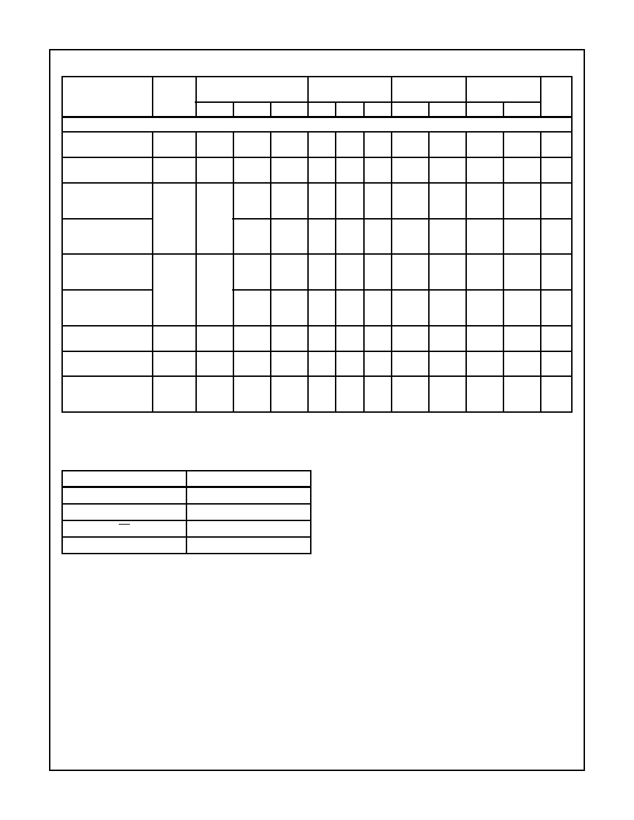
4
HCT TYPES
High Level Input
Voltage
V
IH
-
-
4.5 to
5.5
2
-
-
2
-
2
-
V
Low Level Input
Voltage
V
IL
-
-
4.5 to
5.5
-
-
0.8
-
0.8
-
0.8
V
High Level Output
Voltage
CMOS Loads
V
OH
V
IH
or
V
IL
-0.02
4.5
4.4
-
-
4.4
-
4.4
-
V
High Level Output
Voltage
TTL Loads
-4
4.5
3.98
-
-
3.84
-
3.7
-
V
Low Level Output
Voltage
CMOS Loads
V
OL
V
IH
or
V
IL
0.02
4.5
-
-
0.1
-
0.1
-
0.1
V
Low Level Output
Voltage
TTL Loads
4
4.5
-
-
0.26
-
0.33
-
0.4
V
Input Leakage
Current
I
I
V
CC
to
GND
-
5.5
-
-
±
0.1
-
±
1
-
±
1
µ
A
Quiescent Device
Current
I
CC
V
CC
or
GND
-
5.5
-
-
8
-
80
-
160
µ
A
Additional Quiescent
Device Current Per
Input Pin: 1 Unit Load
I
CC
(Note 2)
V
CC
- 2.1
-
4.5 to
5.5
-
100
360
-
450
-
490
µ
A
NOTE:
2. For dual-supply systems theoretical worst case (V
I
= 2.4V, V
CC
= 5.5V) specification is 1.8mA.
DC Electrical Specifications
(Continued)
PARAMETER
SYMBOL
TEST
CONDITIONS
25
o
C
-40
o
C TO 85
o
C
-55
o
C TO 125
o
C
UNITS
V
I
(V)
I
O
(mA)
V
CC
(V)
MIN
TYP
MAX
MIN
MAX
MIN
MAX
HCT Input Loading Table
INPUT
UNIT LOADS
P0-P3
0.4
MR
1.45
PL
0.85
CPU, CPD
1.45
NOTE: Unit Load is
I
CC
limit specified in DC Electrical
Specifications table, e.g. 360
µ
A max at 25
o
C.
CD54/74HC192, CD54/74HC193, CD54/74HCT193

5
Prerequisite For Switching Specifications
PARAMETER
SYMBOL
V
CC
(V)
25
o
C
-40
o
C TO 85
o
C
-55
o
C TO 125
o
C
UNITS
MIN
TYP
MAX
MIN
MAX
MIN
MAX
HC TYPES
Pulse Width
t
W
2
115
-
-
145
-
175
-
ns
CPU, CPD
4.5
23
-
-
29
-
35
-
ns
192
6
20
-
-
25
-
30
-
ns
t
W
2
100
-
-
125
-
150
-
ns
CPU, CPD
4.5
20
-
-
25
-
30
-
ns
193
6
17
-
-
21
-
26
-
ns
PL
t
W
2
80
-
-
100
-
120
-
ns
4.5
16
-
-
20
-
24
-
ns
6
14
-
-
17
-
20
-
ns
MR
t
W
2
100
-
-
125
-
150
-
ns
4.5
20
-
-
25
-
30
-
ns
6
17
-
-
21
-
26
-
ns
Set-up Time
t
SU
2
80
-
-
100
-
120
-
ns
Pn to PL
4.5
16
-
-
20
-
24
-
ns
6
14
-
-
17
-
20
-
ns
Hold Time
t
H
2
0
-
-
0
-
0
-
ns
Pn to PL
4.5
0
-
-
0
-
0
-
ns
6
0
-
-
0
-
0
-
ns
Hold Time
t
H
2
80
-
-
100
-
120
-
ns
CPD to CPU or
4.5
16
-
-
20
-
24
-
ns
CPU to CPD
6
14
-
-
17
-
20
-
ns
Recovery Time
t
REC
2
80
-
-
100
-
120
-
ns
PL to CPU, CPD
4.5
16
-
-
20
-
24
-
ns
6
14
-
-
17
-
20
-
ns
MR to CPU, CPD
t
REC
2
5
-
-
5
-
5
-
ns
4.5
5
-
-
5
-
5
-
ns
6
5
-
-
5
-
5
-
ns
Maximum Frequency
f
MAX
2
5
-
-
4
-
3
-
MHz
CPU, CPD
4.5
22
-
-
18
-
15
-
MHz
192
6
24
-
-
21
-
18
-
MHz
f
MAX
2
5
-
-
4
-
3
-
MHz
CPU, CPD
4.5
25
-
-
20
-
17
-
MHz
193
6
29
-
-
24
-
20
-
MHz
HCT TYPES
Pulse Width
t
W
2
-
-
-
-
-
-
-
ns
CPU, CPD
4.5
23
-
-
29
-
35
-
ns
192
6
-
-
-
-
-
-
-
ns
CPU, CPD
t
W
2
-
-
-
-
-
-
-
ns
193
4.5
23
-
-
29
-
35
-
ns
6
-
-
-
-
-
-
-
ns
CD54/74HC192, CD54/74HC193, CD54/74HCT193