1
Data sheet acquired from Harris Semiconductor
SCHS188C
Features
∑ Buffered Inputs
∑ Common Three-State Output-Enable Control
∑ Three-State Outputs
∑ Bus Line Driving Capability
∑ Typical Propagation Delay = 13ns at V
CC
= 5V,
C
L
= 15pF, T
A
= 25
o
C (Clock to Output)
∑ Fanout (Over Temperature Range)
- Standard Outputs . . . . . . . . . . . . . . . 10 LSTTL Loads
- Bus Driver Outputs . . . . . . . . . . . . . 15 LSTTL Loads
∑ Wide Operating Temperature Range . . . -55
o
C to 125
o
C
∑ Balanced Propagation Delay and Transition Times
∑ Significant Power Reduction Compared to LSTTL
Logic ICs
∑ HC Types
- 2V to 6V Operation
- High Noise Immunity: N
IL
= 30%, N
IH
= 30% of V
CC
at V
CC
= 5V
∑ HCT Types
- 4.5V to 5.5V Operation
- Direct LSTTL Input Logic Compatibility,
V
IL
= 0.8V (Max), V
IH
= 2V (Min)
- CMOS Input Compatibility, I
l
1
µ
A at V
OL
, V
OH
Description
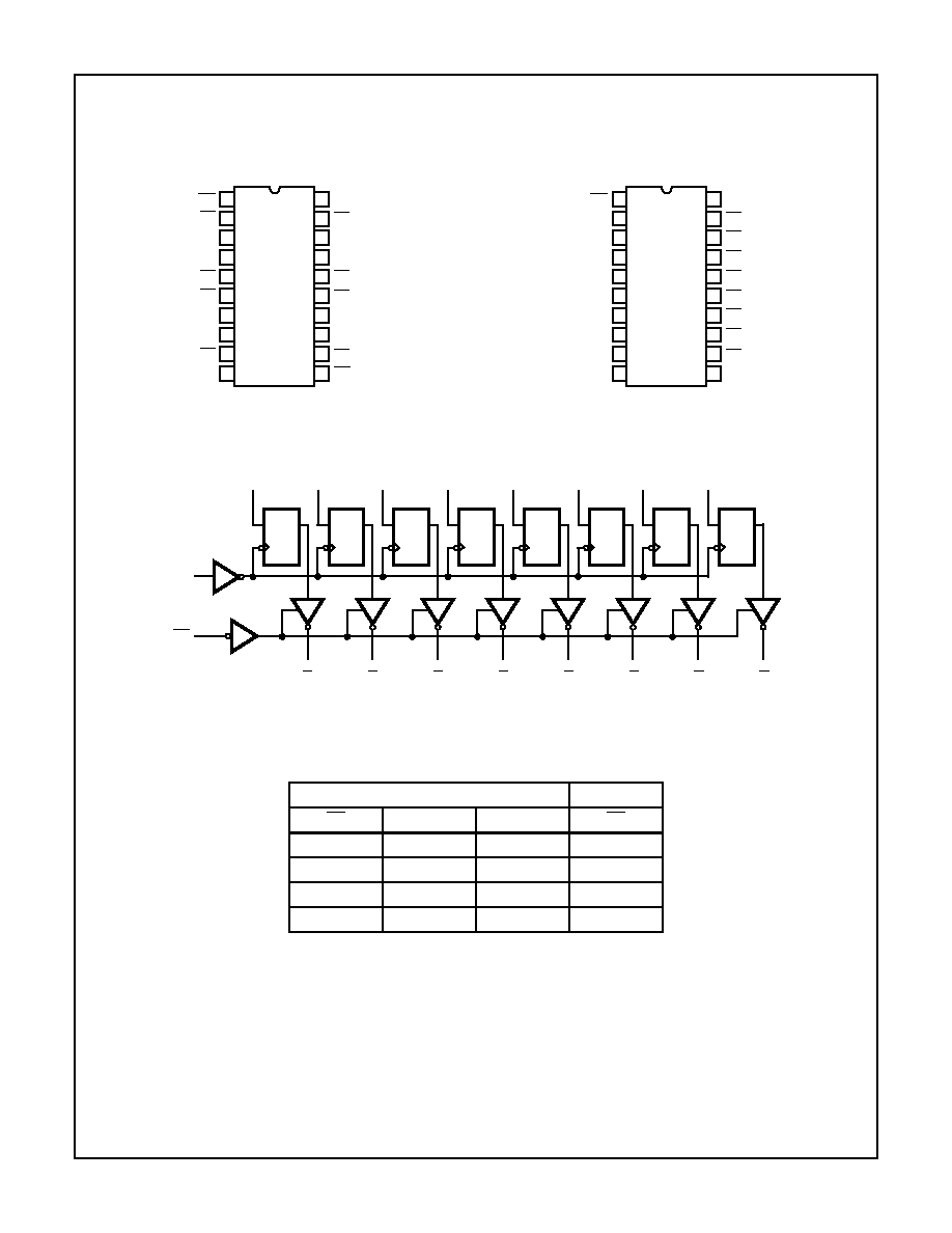
The 'HC534, 'HCT534, 'HC564, and 'HCT564 are high speed
Octal D-Type Flip-Flops manufactured with silicon gate CMOS
technology. They possess the low power consumption of stan-
dard CMOS integrated circuits, as well as the ability to drive
15 LSTTL loads. Due to the large output drive capability and
the three-state feature, these devices are ideally suited for
interfacing with bus lines in a bus organized system. The two
types are functionally identical and differ only in their pinout
arrangements.
The 'HC534, 'HCT534, 'HC564, and 'HCT564 are positive
edge triggered flip-flops. Data at the D inputs, meeting the
setup and hold time requirements, are inverted and trans-
ferred to the Q outputs on the positive going transition of the
CLOCK input. When a high logic level is applied to the OUT-
PUT ENABLE input, all outputs go to a high impedance state,
regardless of what signals are present at the other inputs and
the state of the storage elements.
The HCT logic family is speed, function, and pin compatible
with the standard LS logic family.
Ordering Information
PART NUMBER
TEMP. RANGE
(
o
C)
PACKAGE
CD54HC534F3A
-55 to 125
20 Ld CERDIP
CD54HC564F3A
-55 to 125
20 Ld CERDIP
CD54HCT534F3A
-55 to 125
20 Ld CERDIP
CD54HCT564F3A
-55 to 125
20 Ld CERDIP
CD74HC534E
-55 to 125
20 Ld PDIP
CD74HC564E
-55 to 125
20 Ld PDIP
CD74HC564M
-55 to 125
20 Ld SOIC
CD74HC564M96
-55 to 125
20 Ld SOIC
CD74HCT534E
-55 to 125
20 Ld PDIP
CD74HCT564E
-55 to 125
20 Ld PDIP
CD74HCT564M
-55 to 125
20 Ld SOIC
January 1998 - Revised April 2004
CAUTION: These devices are sensitive to electrostatic discharge. Users should follow proper IC Handling Procedures.
Copyright
©
2004, Texas Instruments Incorporated
CD54/74HC534, CD54/74HCT534,
CD54/74HC564, CD54/74HCT564
High-Speed CMOS Logic Octal D-Type Flip-Flop,
Three-State Inverting Positive-Edge Triggered
[ /Title
(CD74
HC534
,
CD74
HCT53
4,
CD74
HC564
,
CD74
HCT56
2
Functional Diagram
Pinouts
CD54HC534, CD54HCT534
(CERDIP)
CD74HC534, CD74HCT534
(PDIP)
TOP VIEW
CD54HC564, CD54HCT564
(CERDIP)
CD74HC564, CD74HCT564
(PDIP, SOIC)
TOP VIEW
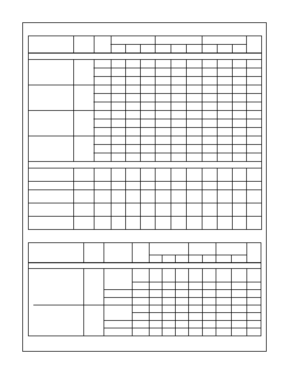
TRUTH TABLE
INPUTS
OUTPUT
OE
CP
Dn
Qn
L
H
L
L
L
H
L
L
X
No Change
H
X
X
Z
H = High Level (Steady State)
L = Low Level (Steady State)
X= Don't Care
= Transition from Low to High Level
Z = High Impedance State
11
12
13
14
15
16
17
18
20
19
10
9
8
7
6
5
4
3
2
1
OE
Q0
D0
D1
Q1
Q2
D3
D2
Q3
GND
V
CC
D7
D6
Q6
Q7
Q5
D5
D4
Q4
CP
11
12
13
14
15
16
17
18
20
19
10
9
8
7
6
5
4
3
2
1
OE
D0
D1
D2
D3
D4
D6
D5
D7
GND
V
CC
Q1
Q2
Q3
Q0
Q4
Q5
Q6
Q7
CP
Q
0
D
0
CP
OE
Q
1
D
1
Q
2
D
2
Q
3
D
3
Q
4
D
4
Q
5
D
5
Q
6
D
6
O
7
D
7
D
Q
D
Q
D
Q
D
Q
D
Q
D
Q
D
Q
D
Q
CP
CP
CP
CP
CP
CP
CP
CP
CD54/74HC534, CD54/74HCT534, CD54/74HC564, CD54/74HCT564
3
Absolute Maximum Ratings
Thermal Information
DC Supply Voltage, V
CC
. . . . . . . . . . . . . . . . . . . . . . . . -0.5V to 7V
DC Input Diode Current, I
IK
For V
I
< -0.5V or V
I
> V
CC
+ 0.5V
. . . . . . . . . . . . . . . . . . . . . .±
20mA
DC Output Diode Current, I
OK
For V
O
< -0.5V or V
O
> V
CC
+ 0.5V
. . . . . . . . . . . . . . . . . . . .±
20mA
DC Drain Current, per Output, I
O
For -0.5V < V
O
< V
CC
+ 0.5V
. . . . . . . . . . . . . . . . . . . . . . . . . .±
35mA
DC Output Source or Sink Current per Output Pin, I
O
For V
O
> -0.5V or V
O
< V
CC
+ 0.5V
. . . . . . . . . . . . . . . . . . . .±
25mA
DC V
CC
or Ground Current, I
CC
. . . . . . . . . . . . . . . . . . . . . . . . .±
50mA
Operating Conditions
Temperature Range, T
A
. . . . . . . . . . . . . . . . . . . . . . -55
o
C to 125
o
C
Supply Voltage Range, V
CC
HC Types . . . . . . . . . . . . . . . . . . . . . . . . . . . . . . . . . . . . .2V to 6V
HCT Types . . . . . . . . . . . . . . . . . . . . . . . . . . . . . . . . .4.5V to 5.5V
DC Input or Output Voltage, V
I
, V
O
. . . . . . . . . . . . . . . . . 0V to V
CC
Input Rise and Fall Time
2V . . . . . . . . . . . . . . . . . . . . . . . . . . . . . . . . . . . . . . 1000ns (Max)
4.5V. . . . . . . . . . . . . . . . . . . . . . . . . . . . . . . . . . . . . . 500ns (Max)
6V . . . . . . . . . . . . . . . . . . . . . . . . . . . . . . . . . . . . . . . 400ns (Max)
Thermal Resistance (Typical, Note 1)
JA
(
o
C/W)
E (PDIP) Package . . . . . . . . . . . . . . . . . . . . . . . . . . . . . .
69
M (SOIC) Package. . . . . . . . . . . . . . . . . . . . . . . . . . . . . .
58
Maximum Junction Temperature . . . . . . . . . . . . . . . . . . . . . . . 150
o
C
Maximum Storage Temperature Range . . . . . . . . . .-65
o
C to 150
o
C
Maximum Lead Temperature (Soldering 10s) . . . . . . . . . . . . . 300
o
C
(SOIC - Lead Tips Only)
CAUTION: Stresses above those listed in "Absolute Maximum Ratings" may cause permanent damage to the device. This is a stress only rating and operation
of the device at these or any other conditions above those indicated in the operational sections of this specification is not implied.
NOTE:
1. The package impedance is calculated in accordance with JESD 51-7.
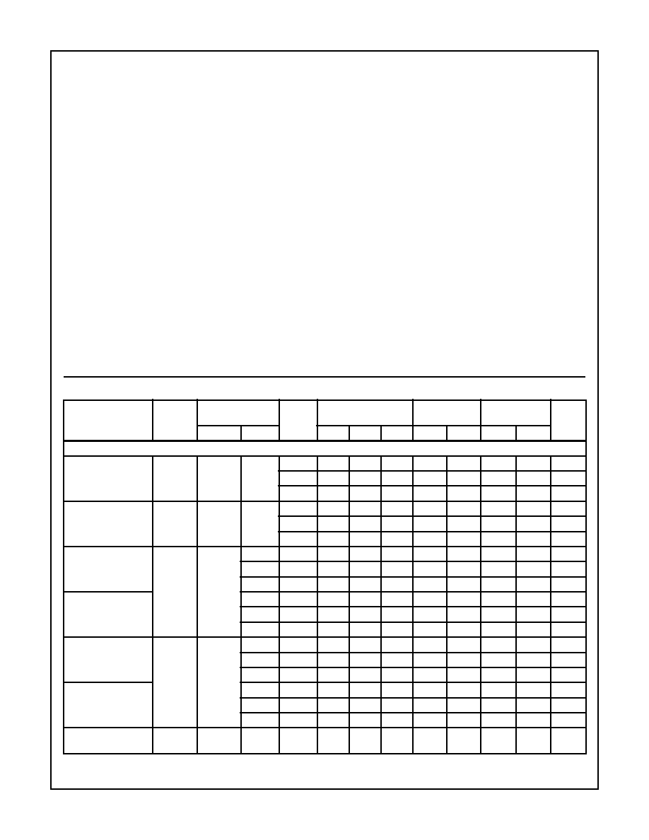
DC Electrical Specifications
PARAMETER
SYMBOL
TEST
CONDITIONS
V
CC
(V)
25
o
C
-40
o
C TO 85
o
C -55
o
C TO 125
o
C
UNITS
V
I
(V)
I
O
(mA)
MIN
TYP
MAX
MIN
MAX
MIN
MAX
HC TYPES
High Level Input
Voltage
V
IH
-
-
2
1.5
-
-
1.5
-
1.5
-
V
4.5
3.15
-
-
3.15
-
3.15
-
V
6
4.2
-
-
4.2
-
4.2
-
V
Low Level Input
Voltage
V
IL
-
-
2
-
-
0.5
-
0.5
-
0.5
V
4.5
-
-
1.35
-
1.35
-
1.35
V
6
-
-
1.8
-
1.8
-
1.8
V
High Level Output
Voltage
CMOS Loads
V
OH
V
IH
or V
IL
-0.02
2
1.9
-
-
1.9
-
1.9
-
V
-0.02
4.5
4.4
-
-
4.4
-
4.4
-
V
-0.02
6
5.9
-
-
5.9
-
5.9
-
V
High Level Output
Voltage
TTL Loads
-
-
-
-
-
-
-
-
-
V
-6
4.5
3.98
-
-
3.84
-
3.7
-
V
-7.8
6
5.48
-
-
5.34
-
5.2
-
V
Low Level Output
Voltage
CMOS Loads
V
OL
V
IH
or V
IL
0.02
2
-
-
0.1
-
0.1
-
0.1
V
0.02
4.5
-
-
0.1
-
0.1
-
0.1
V
0.02
6
-
-
0.1
-
0.1
-
0.1
V
Low Level Output
Voltage
TTL Loads
-
-
-
-
-
-
-
-
-
V
6
4.5
-
-
0.26
-
0.33
-
0.4
V
7.8
6
-
-
0.26
-
0.33
-
0.4
V
Input Leakage
Current
I
I
V
CC
or
GND
-
6
-
-
±
0.1
-
±
1
-
±
1
µ
A
CD54/74HC534, CD54/74HCT534, CD54/74HC564, CD54/74HCT564
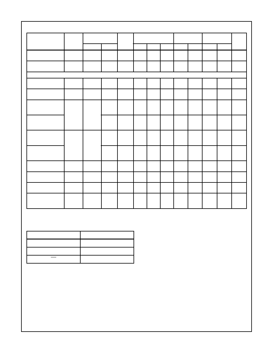
4
Quiescent Device
Current
I
CC
V
CC
or
GND
0
6
-
-
8
-
80
-
160
µ
A
Three- State Leakage
Current
V
IL
or V
IH
V
O
= V
CC
or GND
-
6
-
-
±
0.5
-
±
5.0
-
±
10
µ
A
HCT TYPES
High Level Input
Voltage
V
IH
-
-
4.5 to
5.5
2
-
-
2
-
2
-
V
Low Level Input
Voltage
V
IL
-
-
4.5 to
5.5
-
-
0.8
-
0.8
-
0.8
V
High Level Output
Voltage
CMOS Loads
V
OH
V
IH
or V
IL
-0.02
4.5
4.4
-
-
4.4
-
4.4
-
V
High Level Output
Voltage
TTL Loads
-6
4.5
3.98
-
-
3.84
-
3.7
-
V
Low Level Output
Voltage
CMOS Loads
V
OL
V
IH
or V
IL
0.02
4.5
-
-
0.1
-
0.1
-
0.1
V
Low Level Output
Voltage
TTL Loads
6
4.5
-
-
0.26
-
0.33
-
0.4
V
Input Leakage
Current
I
I
V
CC
and
GND
0
5.5
-
±
0.1
-
±
1
-
±
1
µ
A
Quiescent Device
Current
I
CC
V
CC
or
GND
0
5.5
-
-
8
-
80
-
160
µ
A
Three- State Leakage
Current
V
IL
or V
IH
V
O
= V
CC
or GND
-
5.5
-
-
±
0.5
-
±
5.0
-
±
10
µ
A
Additional Quiescent
Device Current Per
Input Pin: 1 Unit Load
I
CC
(Note 2)
V
CC
-2.1
-
4.5 to
5.5
-
100
360
-
450
-
490
µ
A
NOTE:
2. For dual-supply systems theoretical worst case (V
I
= 2.4V, V
CC
= 5.5V) specification is 1.8mA.
DC Electrical Specifications
(Continued)
PARAMETER
SYMBOL
TEST
CONDITIONS
V
CC
(V)
25
o
C
-40
o
C TO 85
o
C -55
o
C TO 125
o
C
UNITS
V
I
(V)
I
O
(mA)
MIN
TYP
MAX
MIN
MAX
MIN
MAX
HCT Input Loading Table
INPUT
UNIT LOADS
D0 - D7
0.15
CP
0.30
OE
0.55
NOTE: Unit Load is
I
CC
limit specific in DC Electrical Specifications
Table, e.g., 360
µ
A max. at 25
o
C.
CD54/74HC534, CD54/74HCT534, CD54/74HC564, CD54/74HCT564
5
Prerequisite for Switching Specifications
PARAMETER
SYMBOL
V
CC
(V)
25
o
C
-40
o
C TO 85
o
C
-55
o
C TO 125
o
C
UNITS
MIN
TYP
MAX
MIN
TYP
MAX
MIN
TYP
MAX
HC TYPES
Maximum Clock
Frequency
f
MAX
2
6
-
-
5
-
-
4
-
-
MHz
4.5
30
-
-
25
-
-
20
-
-
MHz
6
35
-
-
29
-
-
23
-
-
MHz
Clock Pulse Width
t
W
2
80
-
-
100
-
-
120
-
-
ns
4.5
16
-
-
20
-
-
24
-
-
ns
6
14
-
-
17
-
-
20
-
-
ns
Setup Time
Data to Clock
t
SU
2
60
-
-
75
-
-
90
-
-
ns
4.5
12
-
-
15
-
-
18
-
-
ns
6
10
-
-
13
-
-
15
-
-
ns
Hold Time
Data to Clock
t
H
2
5
-
-
5
-
-
5
-
-
ns
4.5
5
-
-
5
-
-
5
-
-
ns
6
5
-
-
5
-
-
5
-
-
ns
HCT TYPES
Maximum Clock
Frequency
f
MAX
4.5
25
-
-
20
-
-
16
-
-
MHz
Clock Pulse Width
t
W
4.5
20
-
-
25
-
-
30
-
-
ns
Setup Time
Data to Clock
t
SU
4.5
20
-
-
25
-
-
30
-
-
ns
Hold Time
Data to Clock (534)
t
H
4.5
5
-
-
5
-
-
5
-
-
ns
Hold Time
Data to Clock (564)
t
H
4.5
3
-
-
3
-
-
3
-
-
ns
Switching Specifications
C
L
= 50pF, Input t
r
, t
f
= 6ns
PARAMETER
SYMBOL
TEST
CONDITIONS
V
CC
(V)
25
o
C
-40
o
C TO
85
o
C
-55
o
C TO
125
o
C
UNITS
MIN
TYP
MAX
MIN
MAX
MIN
MAX
HC TYPES
Propagation Delay
t
PLH
, t
PHL
C
L
= 50pF
Clock to Output
2
-
-
165
-
205
-
250
ns
4.5
-
-
33
-
41
-
50
ns
C
L
= 15pF
5
-
13
-
-
-
-
-
ns
C
L
= 50pF
6
-
-
28
-
35
-
43
ns
Output Disable to Q (534)
t
PLZ
, t
PHZ
C
L
= 50pF
2
-
-
150
-
190
-
225
ns
4.5
-
-
30
-
38
-
45
ns
C
L
= 15pF
5
-
12
-
-
-
-
-
ns
C
L
= 50pF
6
-
-
26
-
33
-
38
ns
CD54/74HC534, CD54/74HCT534, CD54/74HC564, CD54/74HCT564