 | –≠–ª–µ–∫—Ç—Ä–æ–Ω–Ω—ã–π –∫–æ–º–ø–æ–Ω–µ–Ω—Ç: CDC328ADB | –°–∫–∞—á–∞—Ç—å:  PDF PDF  ZIP ZIP |
CDC328A
1-LINE TO 6-LINE CLOCK DRIVER
WITH SELECTABLE POLARITY
SCAS327B ≠ DECEMBER 1992 ≠ REVISED NOVEMBER 1995
1
POST OFFICE BOX 655303
∑
DALLAS, TEXAS 75265
D
Low Output Skew for Clock-Distribution
and Clock-Generation Applications
D
TTL-Compatible Inputs and Outputs
D
Distributes One Clock Input to Six Clock
Outputs
D
Polarity Control Selects True or
Complementary Outputs
D
Distributed V
CC
and GND Pins Reduce
Switching Noise
D
High-Drive Outputs (≠ 48-mA I
OH
,
48-mA I
OL
)
D
State-of-the-Art
EPIC-
B
TM
BiCMOS Design
Significantly Reduces Power Dissipation
D
Package Options Include Plastic
Small-Outline (D) and Shrink Small-Outline
(DB) Packages
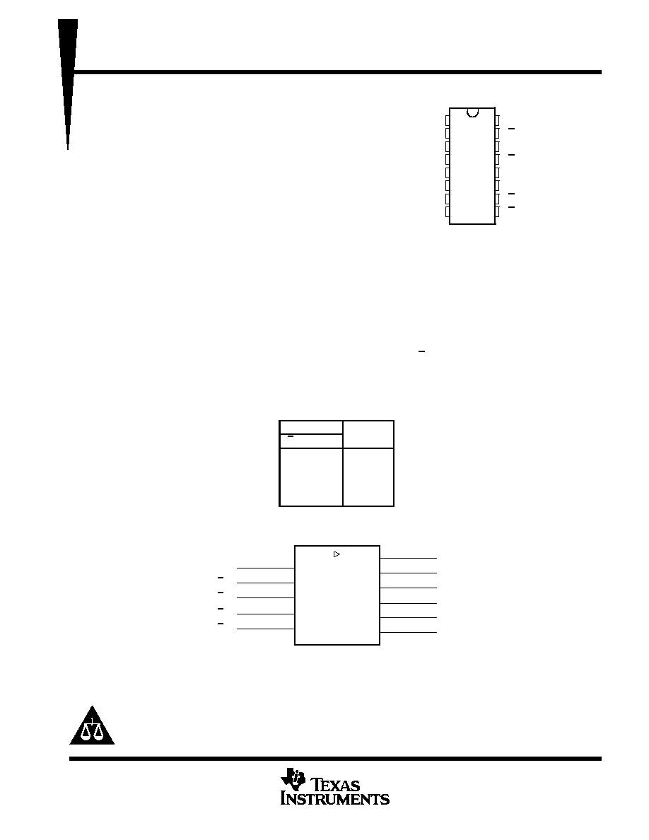
description
The CDC328A contains a clock-driver circuit that distributes one input signal to six outputs with minimum skew
for clock distribution. Through the use of the polarity-control inputs (T/C), various combinations of true and
complementary outputs can be obtained.
The CDC328A is characterized for operation from ≠ 40
∞
C to 85
∞
C.
FUNCTION TABLE
INPUTS
OUTPUT
T/C
A
Y
L
L
L
L
H
H
H
L
H
H
H
L
logic symbol
12
A
N1
15
N2
13
1Y1
16
1
1Y2
2
1
2Y1
3
2
N3
10
N4
9
2Y2
5
2
3Y
6
3
4Y
8
4
1T/C
2T/C
3T/C
4T/C
This symbol is in accordance with ANSI/IEEE Std 91-1984 and IEC Publication 617-12.
Copyright
©
1995, Texas Instruments Incorporated
PRODUCTION DATA information is current as of publication date.
Products conform to specifications per the terms of Texas Instruments
standard warranty. Production processing does not necessarily include
testing of all parameters.
EPIC-
B is a trademark of Texas Instruments Incorporated.
Please be aware that an important notice concerning availability, standard warranty, and use in critical applications of
Texas Instruments semiconductor products and disclaimers thereto appears at the end of this data sheet.
D OR DB PACKAGE
(TOP VIEW)
1
2
3
4
5
6
7
8
16
15
14
13
12
11
10
9
GND
1Y2
2Y1
GND
2Y2
3Y
GND
4Y
1Y1
1T/C
V
CC
2T/C
A
V
CC
3T/C
4T/C
CDC328A
1-LINE TO 6-LINE CLOCK DRIVER
WITH SELECTABLE POLARITY
SCAS327B ≠ DECEMBER 1992 ≠ REVISED NOVEMBER 1995
2
POST OFFICE BOX 655303
∑
DALLAS, TEXAS 75265
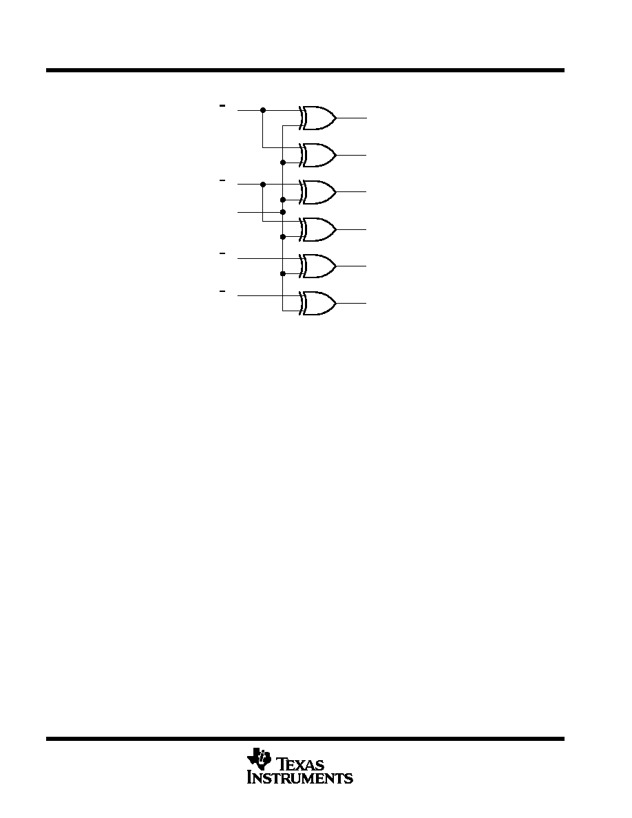
logic diagram (positive logic)
1Y1
1Y2
2Y1
2Y2
3Y
4Y
16
2
3
5
6
8
15
13
12
10
9
1T/C
A
2T/C
3T/C
4T/C
absolute maximum ratings over operating free-air temperature range (unless otherwise noted)
Supply voltage range, V
CC
≠ 0.5 V to 7 V
. . . . . . . . . . . . . . . . . . . . . . . . . . . . . . . . . . . . . . . . . . . . . . . . . . . . . . . . . .
Input voltage range, V
I
(see Note 1)
≠ 0.5 V to 7 V
. . . . . . . . . . . . . . . . . . . . . . . . . . . . . . . . . . . . . . . . . . . . . . . . . .
Voltage range applied to any output in the high state
or power-off state, V
O
(see Note 1)
≠ 0.5 V to V
CC
+ 0.5 V
. . . . . . . . . . . . . . . . . . . . . . . . . . . . . . . . . . . . . . . . .
Current into any output in the low state, I
O
96 mA
. . . . . . . . . . . . . . . . . . . . . . . . . . . . . . . . . . . . . . . . . . . . . . . . . .
Input clamp current, I
IK
(V
I
< 0)
≠18 mA
. . . . . . . . . . . . . . . . . . . . . . . . . . . . . . . . . . . . . . . . . . . . . . . . . . . . . . . . . . .
Output clamp current, I
OK
(V
O
< 0)
≠ 50 mA
. . . . . . . . . . . . . . . . . . . . . . . . . . . . . . . . . . . . . . . . . . . . . . . . . . . . . . .
Maximum power dissipation at T
A
= 55
∞
C (in still air) (see Note 2): D package
0.77 W
. . . . . . . . . . . . . . . . . .
DB package
0.6 W
. . . . . . . . . . . . . . . . . .
Storage temperature range, T
stg
≠ 65
∞
C to 150
∞
C
. . . . . . . . . . . . . . . . . . . . . . . . . . . . . . . . . . . . . . . . . . . . . . . . . .
Stresses beyond those listed under "absolute maximum ratings" may cause permanent damage to the device. These are stress ratings only, and
functional operation of the device at these or any other conditions beyond those indicated under "recommended operating conditions" is not
implied. Exposure to absolute-maximum-rated conditions for extended periods may affect device reliability.
NOTES:
1. The input and output negative-voltage ratings may be exceeded if the input and output clamp-current ratings are observed.
2. The maximum package power dissipation is calculated using a junction temperature of 150
∞
C and a board trace length of 300 mils.
For more information, refer to the
Package Thermal Considerations application note in the 1994 ABT Advanced BiCMOS Technology
Data Book, literature number SCBD002B.
CDC328A
1-LINE TO 6-LINE CLOCK DRIVER
WITH SELECTABLE POLARITY
SCAS327B ≠ DECEMBER 1992 ≠ REVISED NOVEMBER 1995
3
POST OFFICE BOX 655303
∑
DALLAS, TEXAS 75265
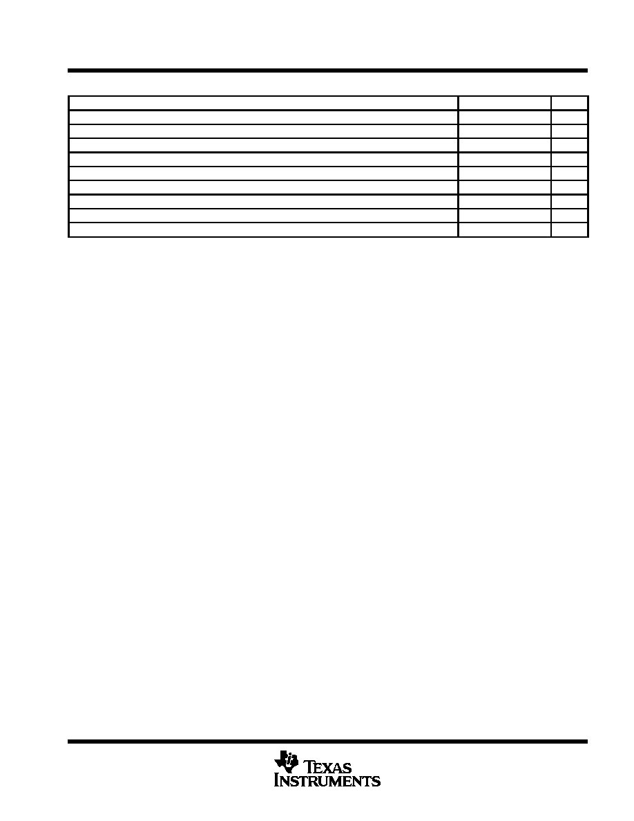
recommended operating conditions (see Note 3)
MIN
NOM
MAX
UNIT
VCC
Supply voltage
4.75
5
5.25
V
VIH
High-level input voltage
2
V
VIL
Low-level input voltage
0.8
V
VI
Input voltage
0
VCC
V
IOH
High-level output current
≠ 48
mA
IOL
Low-level output current
48
mA
t /
v
Input transition rise or fall rate
5
ns / V
fclock
Input clock frequency
100
MHz
TA
Operating free-air temperature
≠ 40
85
∞
C
NOTE 3: Unused inputs must be held high or low to prevent them from floating.
CDC328A
1-LINE TO 6-LINE CLOCK DRIVER
WITH SELECTABLE POLARITY
SCAS327B ≠ DECEMBER 1992 ≠ REVISED NOVEMBER 1995
4
POST OFFICE BOX 655303
∑
DALLAS, TEXAS 75265
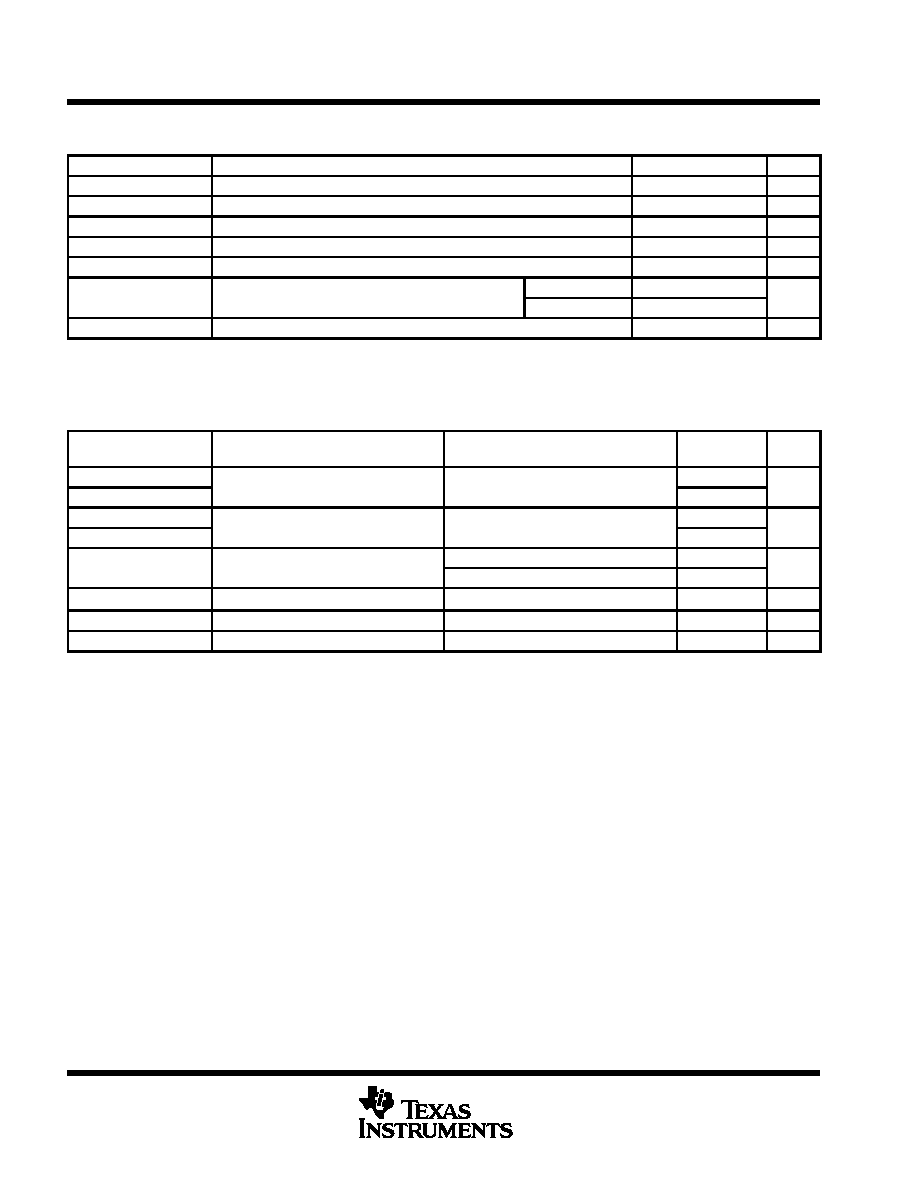
electrical characteristics over recommended operating free-air temperature range (unless
otherwise noted)
PARAMETER
TEST CONDITIONS
MIN
TYP
MAX
UNIT
VIK
VCC = 4.75 V,
II = ≠18 mA
≠1.2
V
VOH
VCC = 4.75 V,
IOH = ≠ 48 mA
2
V
VOL
VCC = 4.75 V,
IOL = 48 mA
0.5
V
II
VCC = 5.25 V,
VI = VCC or GND
±
1
µ
A
IO
VCC = 5.25 V,
VO = 2.5 V
≠15
≠100
mA
ICC
VCC = 5.25 V,
IO = 0,
Outputs high
10
mA
ICC
CC
,
O
,
VI = VCC or GND
Outputs low
40
mA
Ci
VI = 2.5 V or 0.5 V
3
pF
All typical values are at VCC = 5 V, TA = 25
∞
C
Not more than one output should be tested at a time, and the duration of the test should not exceed one second.
switching characteristics over recommended ranges of supply voltage and operating free-air
temperature (see Figures 1 and 2)
PARAMETER
FROM
(INPUT)
TO
(OUTPUT)
MIN
MAX
UNIT
tPLH
A
Any Y
1.7
5
ns
tPHL
A
Any Y
1.5
5
ns
tPLH
T/C
Any Y
1.5
5
ns
tPHL
T/C
Any Y
1.4
5
ns
t k( )
A
Any Y (same phase)
0.5
ns
tsk(o)
A
Any Y (any phase)
1
ns
tsk(p)
A
Any Y
1
ns
tr
Any Y
1.5
ns
tf
Any Y
1.5
ns

CDC328A
1-LINE TO 6-LINE CLOCK DRIVER
WITH SELECTABLE POLARITY
SCAS327B ≠ DECEMBER 1992 ≠ REVISED NOVEMBER 1995
5
POST OFFICE BOX 655303
∑
DALLAS, TEXAS 75265
PARAMETER MEASUREMENT INFORMATION
From Output
Under Test
CL = 50 pF
(see Note A)
LOAD CIRCUIT FOR OUTPUTS
500
tPLH
tPHL
1.5 V
1.5 V
3 V
0 V
1.5 V
1.5 V
VOH
VOL
2 V
0.8 V
0.8 V
tf
tr
Input
(see Note B)
VOLTAGE WAVEFORMS
PROPAGATION DELAY TIMES
Output
NOTES: A. CL includes probe and jig capacitance.
B. All input pulses are supplied by generators having the following characteristics: PRR
10 MHz, ZO = 50
, tr
2.5 ns, tf
2.5 ns.
Figure 1. Load Circuit and Voltage Waveforms