 | –≠–ª–µ–∫—Ç—Ä–æ–Ω–Ω—ã–π –∫–æ–º–ø–æ–Ω–µ–Ω—Ç: CDC9841DW | –°–∫–∞—á–∞—Ç—å:  PDF PDF  ZIP ZIP |
CDC9841
PC MOTHERBOARD CLOCK SYNTHESIZER/DRIVER
WITH 3-STATE OUTPUTS
SCAS458D ≠ DECEMBER 1994 ≠ REVISED APRIL 1996
1
POST OFFICE BOX 655303
∑
DALLAS, TEXAS 75265
D
Four CPU Clock Outputs With
Programmable Frequency
(50 MHz, 60 MHz, and 66 MHz)
D
Six Clock Outputs at Half-CPU Frequency
for PCI
D
One 24-MHz Clock Output
D
One 12-MHz Clock Output
D
Two 14.318-MHz Reference Outputs
D
All Output Clock Frequencies Derived From
a Single 14.31818-MHz Crystal Input
D
LVTTL-Compatible Inputs and Outputs
D
Internal Loop Filters for Phase-Lock Loops
Eliminate the Need for External
Components
D
Operates at 3.3 V
CC
D
Distributed V
CC
and Ground Pins Reduce
Switching Noise
D
Packaged in Plastic Small-Outline Package
description
The CDC9841 is a high-performance clock synthesizer/driver that generates all required clock signals
necessary for a high-performance PC motherboard. The four central processing unit (CPU) clock outputs
(PCLKn) are programmable to one of three frequencies (50 MHz, 60 MHz, or 66 MHz) via the SEL0 and SEL1
control inputs. The six peripheral-component-interconnect (PCI) clock outputs (BCLKn) are half the frequency
of PCLKn and are delayed 1 ns to 4 ns from the rising edge of the CPU clock. In addition, the four fixed-frequency
outputs provide a 24-MHz clock (CLK24), a 12-MHz clock (CLK12), and two buffered copies of the 14.318-MHz
input reference (REF0, REF1).
The CDC9841 generates all output frequencies from a 14.31818-MHz crystal input. A reference clock can be
provided at X1 instead of a crystal input.
Two phase-lock loops (PLLs) generate the CPU clock frequency and the 24-MHz clock frequency. On-chip loop
filters and internal feedback eliminate the need for external components. The PCI and 12-MHz clock
frequencies are derived from the base CPU and 24-MHz clock frequencies, respectively. The PLL circuit can
be bypassed in the TEST mode (i.e., SEL0 = SEL1 = H) to distribute a test clock provided at the X1 input.
Because the CDC9841 is based on PLL circuitry, it requires a stabilization time to achieve phase lock of the PLL.
This stabilization time is required following power up and application of a fixed-frequency, fixed-phase signal
at the X1 input, as well as following any changes to the SELn inputs.
PCLKn and BCLKn provide low-skew/low-jitter clock signals for reliable clock operation. All outputs are 3 state
and are enabled via OE.
Copyright
©
1996, Texas Instruments Incorporated
PRODUCTION DATA information is current as of publication date.
Products conform to specifications per the terms of Texas Instruments
standard warranty. Production processing does not necessarily include
testing of all parameters.
Please be aware that an important notice concerning availability, standard warranty, and use in critical applications of
Texas Instruments semiconductor products and disclaimers thereto appears at the end of this data sheet.
1
2
3
4
5
6
7
8
9
10
11
12
13
14
28
27
26
25
24
23
22
21
20
19
18
17
16
15
V
CC
X1
X2
GND
OE
PCLK0
PCLK1
V
CC
PCLK2
PCLK3
GND
SEL1
SEL0
V
CC
REF0
REF1
V
CC
CLK12
CLK24
GND
BCLK2
BCLK3
V
CC
BCLK4
BCLK5
GND
BCLK1
BCLK0
DW PACKAGE
(TOP VIEW)
CDC9841
PC MOTHERBOARD CLOCK SYNTHESIZER/DRIVER
WITH 3-STATE OUTPUTS
SCAS458D ≠ DECEMBER 1994 ≠ REVISED APRIL 1996
2
POST OFFICE BOX 655303
∑
DALLAS, TEXAS 75265
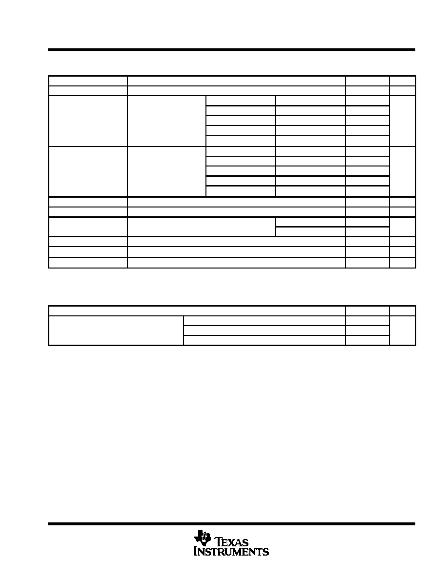
FUNCTION TABLE
OE
SEL0
SEL1
X1
PCLKn
BCLKn
REFn
CLK24
CLK12
L
X
X
14.31818 MHz
Hi-Z
Hi-Z
Hi-Z
Hi-Z
Hi-Z
H
L
L
14.31818 MHz
50 MHz
25 MHz
14.318 MHz
24 MHz
12 MHz
H
L
H
14.31818 MHz
60 MHz
30 MHz
14.318 MHz
24 MHz
12 MHz
H
H
L
14.31818 MHz
66 MHz
33 MHz
14.318 MHz
24 MHz
12 MHz
H
H
H
TCLK
TCLK /2
TCLK /4
TCLK
TCLK /4
TCLK /8
TCLK is a test clock input at the X1 input during test mode.
CDC9841
PC MOTHERBOARD CLOCK SYNTHESIZER/DRIVER
WITH 3-STATE OUTPUTS
SCAS458D ≠ DECEMBER 1994 ≠ REVISED APRIL 1996
3
POST OFFICE BOX 655303
∑
DALLAS, TEXAS 75265
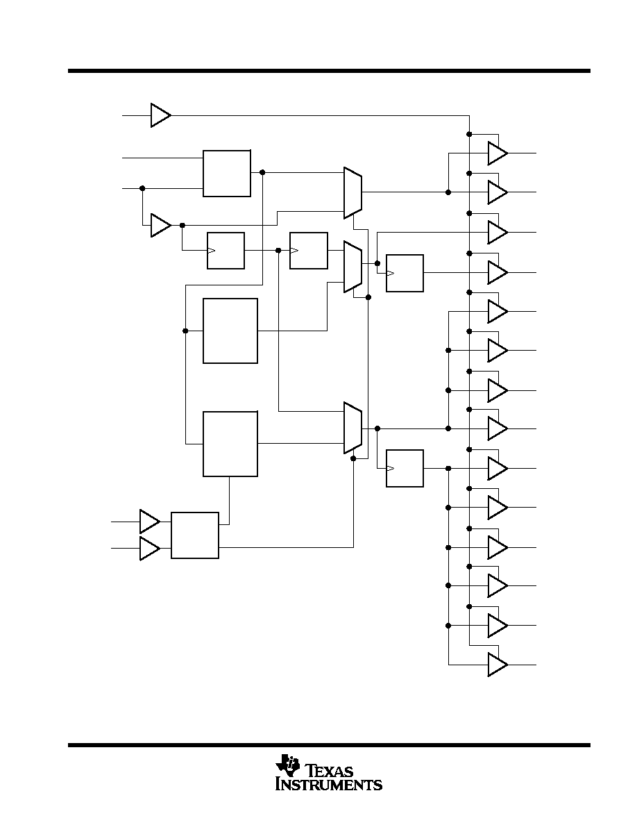
functional block diagram
OE
5
X2
3
OSC
˜
2
REF0
28
REF1
27
CLK24
24
CLK12
25
PCLK0
6
PCLK1
7
9
PCLK3
10
15
BCLK1
16
22
BCLK3
21
19
18
PCLK2
BCLK0
BCLK2
BCLK4
BCLK5
24-MHZ
PLL
CPU CLK
PLL
Select
Logic
SEL0
13
SEL1
12
X1
2
˜
2
˜
2
˜
2
CDC9841
PC MOTHERBOARD CLOCK SYNTHESIZER/DRIVER
WITH 3-STATE OUTPUTS
SCAS458D ≠ DECEMBER 1994 ≠ REVISED APRIL 1996
4
POST OFFICE BOX 655303
∑
DALLAS, TEXAS 75265
absolute maximum ratings over operating free-air temperature range (unless otherwise noted)
Supply voltage range, V
CC
≠ 0.5 V to 4.6 V
. . . . . . . . . . . . . . . . . . . . . . . . . . . . . . . . . . . . . . . . . . . . . . . . . . . . . . . . .
Input voltage range, V
I
(see Note 1)
≠ 0.5 V to 4.6 V
. . . . . . . . . . . . . . . . . . . . . . . . . . . . . . . . . . . . . . . . . . . . . . . . .
Voltage range applied to any output in the high state or power-off state,
V
O
(see Note 1)
≠ 0.5 V to V
CC
+ 0.5 V
. . . . . . . . . . . . . . . . . . . . . . . . . . . . . . . . . . . . . . . . . . . . . . . . . . . . . . . . . .
Current into any output in the low state, I
O
2
I
OHmax
. . . . . . . . . . . . . . . . . . . . . . . . . . . . . . . . . . . . . . . . . . . . .
Input clamp current, I
IK
(V
I
< 0)
≠ 18 mA
. . . . . . . . . . . . . . . . . . . . . . . . . . . . . . . . . . . . . . . . . . . . . . . . . . . . . . . . . . .
Output clamp current, I
OK
(V
O
< 0)
≠ 50 mA
. . . . . . . . . . . . . . . . . . . . . . . . . . . . . . . . . . . . . . . . . . . . . . . . . . . . . . . .
Maximum power dissipation at T
A
= 55
∞
C (in still air) (see Note 2)
1.2 W
. . . . . . . . . . . . . . . . . . . . . . . . . . . . . . .
Storage temperature range, T
stg
≠ 65
∞
C to 150
∞
C
. . . . . . . . . . . . . . . . . . . . . . . . . . . . . . . . . . . . . . . . . . . . . . . . . . .
Stresses beyond those listed under "absolute maximum ratings" may cause permanent damage to the device. These are stress ratings only, and
functional operation of the device at these or any other conditions beyond those indicated under "recommended operating conditions" is not
implied. Exposure to absolute-maximum-rated conditions for extended periods may affect device reliability.
NOTES:
1. The input and output negative-voltage ratings may be exceeded if the input and output clamp-current ratings are observed.
2. The maximum package power dissipation is calculated using a junction temperature of 150
∞
C and a board trace length of 750 mils.
For more information, refer to the
Package Thermal Considerations application note in the 1994 ABT Advanced BiCMOS Technology
Data Book, literature number SCBD002B.
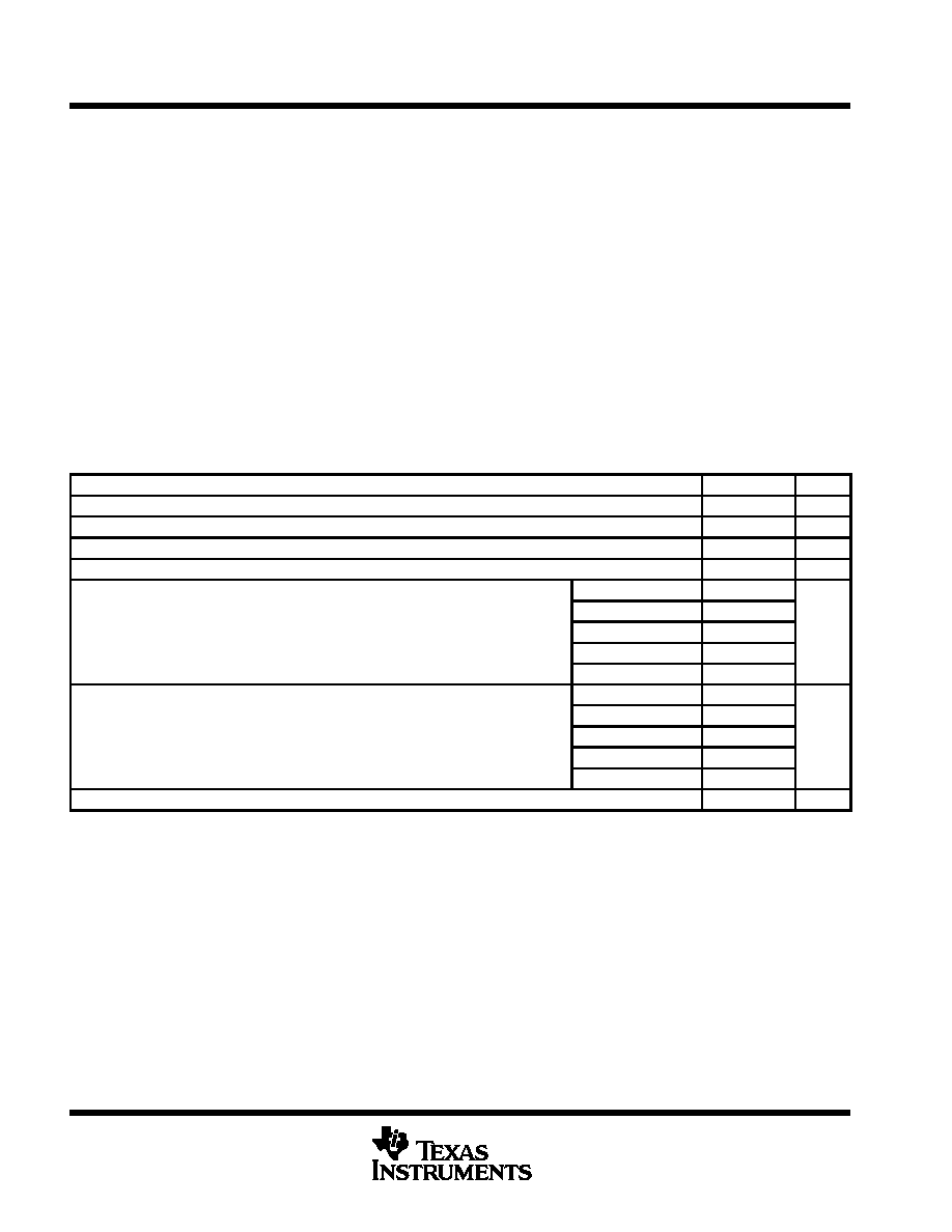
recommended operating conditions (see Note 3)
MIN
MAX
UNIT
VCC
Supply voltage
3.135
3.6
V
VIH
High-level input voltage
2
V
VIL
Low-level input voltage
0.8
V
VI
Input voltage
0
VCC
V
REF0
≠ 12
REF1
≠ 8
IOH
High-level output current
PCLKn
≠ 6
mA
BCLKn
≠ 12
CLK24, CLK12
≠ 4
REF0
12
REF1
8
IOL
Low-level output current
PCLKn
6
mA
BCLKn
12
CLK24, CLK12
4
TA
Operating free-air temperature
0
70
∞
C
NOTE 3: Unused inputs must be held high or low to prevent them from floating.
CDC9841
PC MOTHERBOARD CLOCK SYNTHESIZER/DRIVER
WITH 3-STATE OUTPUTS
SCAS458D ≠ DECEMBER 1994 ≠ REVISED APRIL 1996
5
POST OFFICE BOX 655303
∑
DALLAS, TEXAS 75265
electrical characteristics over recommended operating free-air temperature range (unless
otherwise noted)
PARAMETER
TEST CONDITIONS
MIN
MAX
UNIT
VIK
VCC = 3.135 V,
II = ≠18 mA
≠1.2
V
IOH = ≠ 12 mA
REF0
2.5
IOH = ≠ 8 mA
REF1
2.5
VOH
VCC = 3.135 V
IOH = ≠ 6 mA
PCLKn
2.5
V
OH
CC
IOH = ≠ 12 mA
BCLKn
2.5
IOH = 4 mA
CLK24 CLK12
2 5
IOH = ≠ 4 mA
CLK24, CLK12
2.5
IOL = 12 mA
REF0
0.4
IOL = 8 mA
REF1
0.4
VOL
VCC = 3.135 V
IOL = 6 mA
PCLKn
0.4
V
OL
CC
IOL = 12 mA
BCLKn
0.4
IOL = 4 mA
CLK24 CLK12
0 4
IOL = 4 mA
CLK24, CLK12
0.4
II
VCC = 3.6 V,
VI = VCC or GND
±
1
µ
A
IOZ
VCC = 3.6 V,
VO = VCC or GND
±
10
µ
A
ICC
VCC = 3.6 V,
IO = 0,
Outputs enabled
50
mA
ICC
CC
,
VI = VCC or GND
O
,
Outputs disabled
1
mA
Ci
VI = VCC or GND
pF
Co
VO = VCC or GND
pF
Cpd
VI = 3 V or 0
pF
Device in normal operating mode with no load on outputs
timing requirements over recommended ranges of supply voltage and operating free-air
temperature
MIN
MAX
UNIT
After SEL1, SEL0
5
Stabilization time
After OE
5
ms
After power up
5
Time required for the integrated PLL circuit to obtain phase lock of its feedback signal to its reference signal. In order for phase lock to be obtained,
a fixed-frequency, fixed-phase reference signal must be present at X1. Until phase lock is obtained, the specifications for propagation delay and
skew parameters given in the switching characteristics table are not applicable.