16-Bit Registered Transceiver
CY74FCT163652
SCCS052 - March 1997 - Revised March 2000
Data sheet acquired from Cypress Semiconductor Corporation.
Data sheet modified to remove devices not offered.
Copyright
©
2000, Texas Instruments Incorporated
Features
∑ Low power, pin-compatible replacement for LCX and
LPT families
∑ 5V tolerant inputs and outputs
∑ 24 mA balanced drive outputs
∑ Power-off disable outputs permits live insertion
∑ Edge-rate control circuitry for reduced noise
∑ FCT-C speed at 4.6 ns
∑ Latch-up performance exceeds JEDEC standard no. 17
∑ ESD > 2000V per MIL-STD-883D, Method 3015
∑ Typical output skew < 250 ps
∑ Industrial temperature range of ≠40∞C to +85∞C
∑ TSSOP (19.6-mil pitch) or SSOP (25-mil pitch)
∑ Typical V
olp
(ground bounce) performance exceeds Mil
Std 883D
∑ V
CC
= 2.7V to 3.6V
Functional Description
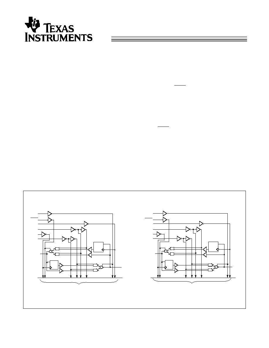
The CY74FCT163652 is a 16-bit, high-speed, low-power,
registered transceiver that is organized as two independent
8-bit bus transceivers with three-state D-type registers and
control circuitry arranged for multiplexed transmission of data
directly from the input bus or from the internal storage
registers. OEAB and OEBA control pins are provided to control
the transceiver functions. SAB and SBA control pins are
provided to select either real-time or stored data transfer.
Data on the A or B data bus, or both, can be stored in the
internal D flip-flops by LOW-to-HIGH transitions at the
appropriate clock pins (CLKAB or CLKBA), regardless of the
select or enable control pins. When SAB and SBA are in the
real-time transfer mode, it is also possible to store data without
using the internal D-type flip-flops by simultaneously enabling
OEAB and OEBA. In this configuration, each output reinforces
its input. Thus, when all other data sources to the two sets of
bus lines are at high impedance, each set of bus lines will
remain at its last state.
The CY74FCT163652 has 24-mA balanced output drivers
with current limiting resistors in the outputs. This reduces the
need for external terminating resistors and provides for
minimal undershoot and reduced ground bounce. The inputs
and outputs were designed to be capable of being driven by
5.0V buses, allowing them to be used in mixed voltage
systems as translators. The outputs are also designed with a
power-off disable feature enabling them to be used in
applications requiring live insertion.
TO 7 OTHER CHANNELS
1
OEAB
C
D
1
A
1
1
OEBA
1
CLKBA
1
CLKAB
1
SBA
B REG
C
D
A REG
1
B
1
1
SAB
2
OEAB
2
SAB
2
OEBA
2
CLKBA
2
CLKAB
2
SBA
2
B
1
2
A
1
C
D
B REG
C
D
A REG
TO 7 OTHER CHANNELS
Logic Block Diagrams
CY74FCT163652
2
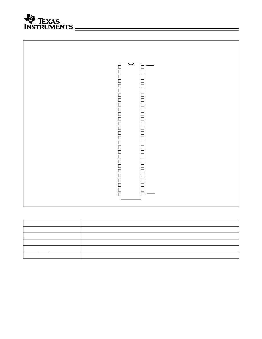
Pin Configuration
SSOP/TSSOP
Top View
FCT16652≠1
GND
1
OEAB
1
CLKAB
1
SAB
1
A
1
1
A
2
1
CLKBA
1
SBA
1
B
1
1
OEBA
GND
GND
V
CC
1
A
3
V
CC
GND
1
A
4
1
A
5
1
A
6
1
A
7
1
A
8
2
A
1
2
A
2
2
A
3
2
A
4
GND
2
A
5
2
A
6
V
CC
2
A
7
2
A
8
2
SAB
2
CLKAB
1
2
3
4
5
6
7
8
9
10
11
12
13
14
15
16
17
18
19
20
21
22
23
24
25
26
27
28
56
55
54
53
52
51
50
49
48
47
46
45
44
43
42
41
40
39
38
37
36
35
34
33
32
31
30
29
GND
2
OEAB
1
B
2
1
B
3
1
B
4
1
B
5
1
B
6
1
B
7
1
B
8
2
B
1
2
B
2
2
B
3
GND
2
B
4
2
B
5
2
B
6
V
CC
2
B
7
2
B
8
GND
2
SBA
2
CLKBA
2
OEBA
Pin Description
Name
Description
A
Data Register A Inputs, Data Register B Outputs
B
Data Register B Inputs, Data Register A Outputs
CLKAB, CLKBA
Clock Pulse Inputs
SAB, SBA
Output Data Source Select Inputs
OEAB, OEBA
Output Enable Inputs
CY74FCT163652
3
Function Table
[1]
Inputs
Data I/O
[2]
Operation or Function
OEAB
OEBA
CLKAB
CLKBA
SAB
SBA
A
B
L
L
H
H
H or L
H or L
X
X
X
X
Input
Input
Isolation
Store A and B Data
X
H
H
H
H or L
X
X
[3]
X
X
Input
Input
Unspecified
[2]
Output
Store A, Hold B
Store A in Both Registers
L
L
X
L
H or L
X
X
X
X
[3]
Unspecified
[2]
Input
Input
Hold A, Store B
Store B in both Registers
L
L
L
L
X
X
X
H or L
X
X
L
H
Output
Input
Real Time B Data to A Bus
Stored B Data to A Bus
H
H
H
H
X
H or L
X
X
L
H
X
X
Input
Output
Real Time A Data to B Bus
Stored A Data to B Bus
H
L
H or L
H or L
H
H
Output
Output
Stored A Data to B Bus and
Stored B Data to A Bus
Notes:
1.
H = HIGH Voltage Level, L = LOW Voltage Level, X = Don't Care,
= LOW-to-HIGH Transition
2.
The data output functions may be enabled or disabled by various signals at the OEAB or OEBA inputs. Data input functions are always enabled, i.e., data at
the bus pins will be stored on every LOW-to-HIGH transition on the clock inputs.
3.
Select control=L; clocks can occur simultaneously.
Select control=H; clocks must be staggered to load both registers.
CY74FCT163652
4
Maximum Ratings
[4]
(Above which the useful life may be impaired. For user
guidelines, not tested.)
Storage Temperature ..............................
-
55
∞
C to +125
∞
C
Ambient Temperature with
Power Applied ..........................................
-
55
∞
C to +125
∞
C
Supply Voltage Range ..................................... 0.5V to +4.6V
DC Input Voltage
.................................................-
0.5V to +7.0V
DC Output Voltage
..............................................-
0.5V to +7.0V
DC Output Current
(Maximum Sink Current/Pin)
...........................-
60 to +120 mA
Power Dissipation .......................................................... 1.0W
Static Discharge Voltage............................................>2001V
(per MIL-STD-883, Method 3015)
Note:
4.
Stresses greater than those listed under Maximum Ratings may cause permanent damage to the device. This is a stress rating only and functional operation of
the device at these or any other conditions above those indicated in the operational sections of this specification is not implied. Exposure to absolute maximum
rating conditions for extended periods may affect reliability.
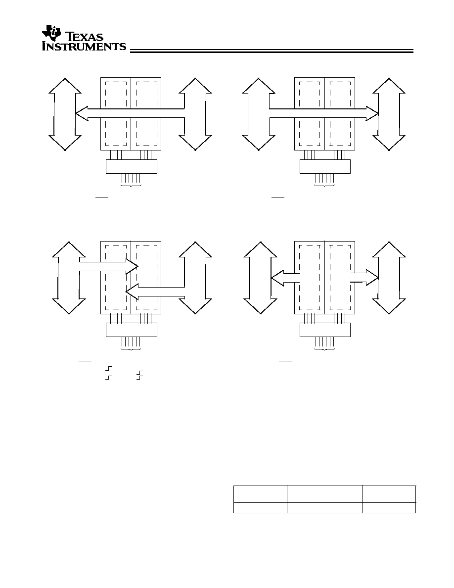
BUS B
BUS A
OEAB
L
OEBA
L
CLKAB
X
SAB
X
BUS B
BUS A
OEAB
X
L
L
OEBA
H
X
H
CLKAB
X
SAB
X
X
X
SBA
X
X
X
BUS B
BUS A
OEAB
H
OEBA
L
SAB
L
SBA
X
BUS A
BUS A
OEAB
H
OEBA
L
SAB
H
SBA
H
Real-Time Transfer
Bus B to BusA
Real-Time Transfer
BusA to Bus B
Storage from
A and/or B
Transfer Stored Data
to A and/or B
CLKBA
X
CLKAB
X
CLKBA
X
SBA
L
CLKBA
X
CLKAB
H or L
CLKBA
H or L
Operating Range
Range
Ambient
Temperature
V
CC
Industrial
≠40
∞
C to +85
∞
C
2.7V to 3.6V
CY74FCT163652
5
Electrical Characteristics
Over the Operating Range V
CC
=2.7V to 3.6V
Parameter
Description
Test Condition
Min.
Typ.
[5]
Max.
Unit
V
IH
Input HIGH Voltage
All Inputs
2.0
5.5
V
V
IL
Input LOW Voltage
0.8
V
V
H
Input Hysteresis
[6]
100
mV
V
IK
Input Clamp Diode Voltage
V
CC
=Min., I
IN
=
-
18 mA
-
0.7
-
1.2
V
I
IH
Input HIGH Current
V
CC
=Max., V
I
=5.5V
±
1
µ
A
I
IL
Input LOW Current
V
CC
=Max., V
I
=GND
±
1
µ
A
I
OZH
High Impedance Output Current
(Three-State Output pins)
V
CC
=Max., V
OUT
=5.5V
±
1
µ
A
I
OZL
High Impedance Output Current
(Three-State Output pins)
V
CC
=Max., V
OUT
=GND
±
1
µ
A
I
ODL
Output LOW Dynamic Current
[7]
V
CC
=3.3V, V
IN
=V
IH
or V
IL
, V
OUT
=1.5V
45
180
mA
I
ODH
Output HIGH Dynamic Current
[7]
V
CC
=3.3V, V
IN
=V
IH
or V
IL
, V
OUT
=1.5V
≠45
≠180
mA
V
OH
Output HIGH Voltage
V
CC
=Min., I
OH
= ≠0.1 mA
V
CC
≠0.2
V
V
CC
=3.0V, I
OH
= ≠8 mA
2.4
[8]
3.0
V
CC
=3.0V, I
OH
= ≠24 mA
2.0
3.0
V
OL
Output LOW Voltage
V
CC
=Min., I
OL
= 0.1mA
0.2
V
V
CC
=Min., I
OL
= 24 mA
0.3
0.5
I
OS
Short Circuit Current
[7]
V
CC
=Max., V
OUT
=GND
≠60
≠135
≠240
mA
I
OFF
Power-Off Disable
[7]
V
CC
=0V, V
OUT
4.5V
±
100
µ
A
Capacitance
[6]
(T
A
= +25∞C, f = 1.0 MHz)
Parameter
Description
Test Conditions
Typ.
Max.
Unit
C
IN
Input Capacitance
V
IN
= 0V
4.5
6.0
pF
C
OUT
Output Capacitance
V
OUT
= 0V
5.5
8.0
pF
Notes:
5.
Typical values are at V
CC
=3.3V, +25
∞
C ambient.
6.
This parameter is specified but not tested.
7.
Not more than one output should be shorted at a time. Duration of short should not exceed one second. The use of high-speed test apparatus and/or sample
and hold techniques are preferable in order to minimize internal chip heating and more accurately reflect operational values. Otherwise prolonged shorting of
a high output may raise the chip temperature well above normal and thereby cause invalid readings in other parametrics tests. In any sequence of parameter
tests, I
OS
tests should be performed last.
8.
V
OH
=V
CC
≠0.6V at rated current.