16-Bit Latches
CY74FCT16373T
CY74FCT162373T
SCCS054C - August 1994 - Revised October 2003
Data sheet acquired from Cypress Semiconductor Corporation.
Data sheet modified to remove devices not offered.
Copyright
©
2003, Texas Instruments Incorporated
Features
∑ I
off
supports partial-power-down mode operation
∑ Edge-rate control circuitry for significantly improved
noise characteristics
∑ Typical output skew < 250 ps
∑ ESD > 2000V
∑ TSSOP (19.6-mil pitch) and SSOP (25-mil pitch)
packages
∑ Industrial temperature range of
-
40∞C to +85∞C
∑ V
CC
= 5V
±
10%
CY74FCT16373T Features:
∑ 64 mA sink current, 32 mA source current
∑ Typical V
OLP
(ground bounce) <1.0V at V
CC
= 5V,
T
A
= 25∞C
CY74FCT162373T Features:
∑ Balanced 24 mA output drivers
∑ Reduced system switching noise
∑ Typical V
OLP
(ground bounce) <0.6V at V
CC
= 5V,
T
A
= 25∞C
Functional Description
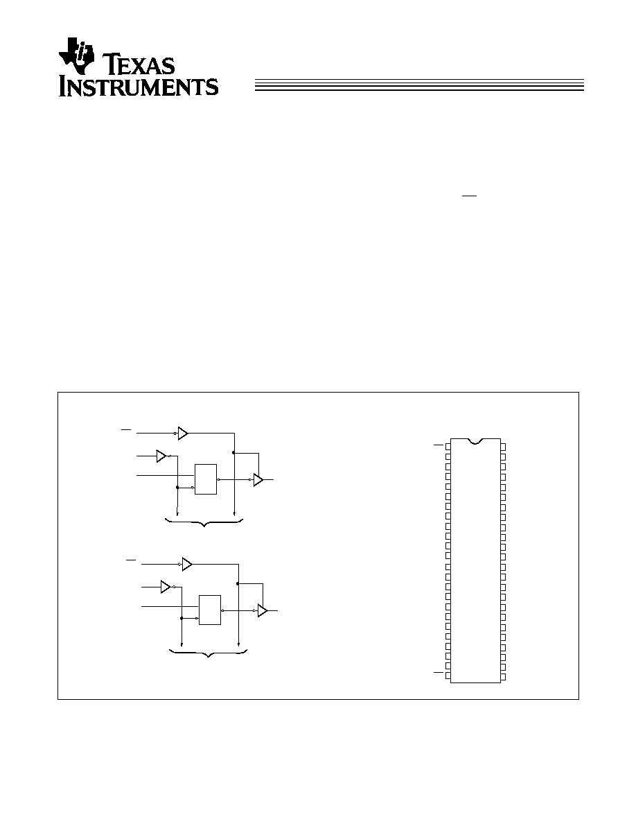
CY74FCT16373T and CY74FCT162373T are 16-bit D-type
latches designed for use in bus applications requiring high
speed and low power. These devices can be used as two
independent 8-bit latches or as a single 16-bit latch by
connecting the Output Enable (OE) and Latch (LE) inputs.
Flow-through pinout and small shrink packaging aid in
simplifying board layout.
This
device
is
fully
specified
for
partial-power-down
applications using I
off
. The I
off
circuitry disables the outputs,
preventing damaging current backflow through the device
when it is powered down.
The
CY74FCT16373T
is
ideally
suited
for
driving
high-capacitance loads and low-impedance backplanes.
The CY74FCT162373T has 24-mA balanced output drivers
with current limiting resistors in the outputs. This reduces the
need for external terminating resistors and provides for
minimal undershoot and reduced ground bounce. The
CY74FCT162373T is ideal for driving transmission lines.
Logic Block Diagrams
Pin Configuration
D
C
1
OE
FCT162373-1
1
LE
1
D
1
1
O
1
TO 7 OTHER CHANNELS
D
C
2
OE
FCT162373-2
2
LE
2
D
1
2
O
1
GND
1
2
3
4
5
6
7
8
9
10
11
12
33
32
31
30
29
25
26
27
28
36
35
1
OE
34
SSOP/TSSOP/TVSOP
Top View
13
14
15
16
17
18
19
20
21
22
23
24
45
44
43
42
41
37
38
39
40
48
47
46
1
O
1
1
O
2
1
O
3
1
O
4
1
D
1
1
D
2
1
D
3
1
D
4
1
LE
GND
GND
V
CC
1
O
7
1
O
8
1
O
5
1
O
6
1
D
5
1
D
6
1
D
7
1
D
8
V
CC
GND
GND
2
O
3
2
O
4
2
O
1
2
O
2
2
D
1
2
D
2
2
D
3
2
D
4
GND
GND
V
CC
2
O
7
2
O
8
2
O
5
2
O
6
2
D
5
2
D
6
2
D
7
2
D
8
V
CC
GND
2
OE
2
LE
FCT162373-3
TO 7 OTHER CHANNELS
CY74FCT16373T
CY74FCT162373T
2
Maximum Ratings
[2, 3]
(Above which the useful life may be impaired. For user
guidelines, not tested.)
Storage Temperature ...................... Com'l
-
55
∞
C to +125
∞
C
Ambient Temperature with
Power Applied................................. Com'l
-
55
∞
C to +125
∞
C
DC Input Voltage
.................................................-
0.5V to +7.0V
DC Output Voltage
..............................................-
0.5V to +7.0V
DC Output Current
(Maximum Sink Current/Pin)
...........................-
60 to +120 mA
Power Dissipation .......................................................... 1.0W
Static Discharge Voltage............................................>2001V
(per MIL-STD-883, Method 3015)
Pin Description
Name
Description
D
Data Inputs
LE
Latch Enable Inputs (Active HIGH)
OE
Output Enable Inputs (Active LOW)
O
Three-State Outputs
Function Table
[1]
Inputs
Outputs
D
LE
OE
O
H
H
L
H
L
H
L
L
X
L
L
Q
0
X
X
H
Z
Operating Range
Range
Ambient
Temperature
V
CC
Industrial
-
40
∞
C to +85
∞
C
5V
±
10%
Electrical Characteristics
Over the Operating Range
Parameter
Description
Test Conditions
Min.
Typ.
[4]
Max.
Unit
V
IH
Input HIGH Voltage
2.0
V
V
IL
Input LOW Voltage
0.8
V
V
H
Input Hysteresis
[5]
100
mV
V
IK
Input Clamp Diode Voltage
V
CC
=Min., I
IN
=
-
18 mA
-
0.7
-
1.2
V
I
IH
Input HIGH Current
V
CC
=Max., V
I
=V
CC
±
1
µ
A
I
IL
Input LOW Current
V
CC
=Max., V
I
=GND
±
1
µ
A
I
OZH
High Impedance Output Current
(Three-State Output pins)
V
CC
=Max., V
OUT
=2.7V
±
1
µ
A
I
OZL
High Impedance Output Current
(Three-State Output pins)
V
CC
=Max., V
OUT
=0.5V
±
1
µ
A
I
OS
Short Circuit Current
[6]
V
CC
=Max., V
OUT
=GND
-
80
-
140
-
200
mA
I
O
Output Drive Current
[6]
V
CC
=Max., V
OUT
=2.5V
-
50
-
180
mA
I
OFF
Power-Off Disable
V
CC
=0V, V
OUT
4.5V
[7]
±
1
µ
A
Output Drive Characteristics for CY74FCT16373T
Parameter
Description
Test Conditions
Min.
Typ.
[4]
Max.
Unit
V
OH
Output HIGH Voltage
V
CC
=Min., I
OH
=
-
3 mA
2.5
3.5
V
V
CC
=Min., I
OH
=
-
15 mA
2.4
3.5
V
V
CC
=Min., I
OH
=
-
32 mA
2.0
3.0
V
V
OL
Output LOW Voltage
V
CC
=Min., I
OL
=64 mA
0.2
0.55
V
Notes:
1.
H = HIGH Voltage Level. L = LOW Voltage Level. X = Don't Care. Z = High Impedance. Q
0
=Previous state of flip-flop.
2.
Operation beyond the limits set forth may impair the useful life of the device. Unless otherwise noted, these limits are over the operating free-air temperature
range.
3.
Unused inputs must always be connected to an appropriate logic voltage level, preferably either V
CC
or ground.
4.
Typical values are at V
CC
=5.0V, T
A
= +25∞C ambient.
5.
This parameter is specified but not tested.
6.
Not more than one output should be shorted at a time. Duration of short should not exceed one second. The use of high-speed test apparatus and/or sample
and hold techniques are preferable in order to minimize internal chip heating and more accurately reflect operational values. Otherwise prolonged shorting of
a high output may raise the chip temperature well above normal and thereby cause invalid readings in other parametric tests. In any sequence of parameter
tests, I
OS
tests should be performed last.
7.
Tested at +25∞C.
CY74FCT16373T
CY74FCT162373T
3
Output Drive Characteristics for CY74FCT162373T
Parameter
Description
Test Conditions
Min.
Typ.
[4]
Max.
Unit
I
ODL
Output LOW Current
[6]
V
CC
=5V, V
IN
=V
IH
or V
IL
, V
OUT
=1.5V
60
115
150
mA
I
ODH
Output HIGH Current
[6]
V
CC
=5V, V
IN
=V
IH
or V
IL
, V
OUT
=1.5V
-
60
-
115
-
150
mA
V
OH
Output HIGH Voltage
V
CC
=Min., I
OH
=
-
24 mA
2.4
3.3
V
V
OL
Output LOW Voltage
V
CC
=Min., I
OL
=24 mA
0.3
0.55
V
Capacitance
[5]
(T
A
= +25∞C, f = 1.0 MHz)
Parameter
Description
Test Conditions
Typ.
[4]
Max.
Unit
C
IN
Input Capacitance
V
IN
= 0V
4.5
6.0
pF
C
OUT
Output Capacitance
V
OUT
= 0V
5.5
8.0
pF
Power Supply Characteristics
Parameter
Description
Test Conditions
Typ.
[4]
Max.
Unit
I
CC
Quiescent Power Supply Current V
CC
=Max.
V
IN
0.2V,
V
IN
V
CC
-
0.2V
5
500
µ
A
I
CC
Quiescent Power Supply Current
(TTL inputs HIGH)
V
CC
=Max.
V
IN
=3.4V
[8]
0.5
1.5
mA
I
CCD
Dynamic Power Supply
Current
[9]
V
CC
=Max., One Input
Toggling, 50% Duty Cycle,
Outputs Open, OE=GND
V
IN
=V
CC
or
V
IN
=GND
60
100
µ
A/MHz
I
C
Total Power Supply Current
[10]
V
CC
=Max., f
1
=10 MHz,
50% Duty Cycle, Outputs
Open, One Bit Toggling,
OE=GND, LE=V
CC
V
IN
=V
CC
or
V
IN
=GND
0.6
1.5
mA
V
IN
=3.4V or
V
IN
=GND
0.9
2.3
mA
V
CC
=Max., f
1
=2.5 MHz,
50% Duty Cycle, Outputs
Open, Sixteen Bits Toggling,
OE=GND, LE=V
CC
V
IN
=V
CC
or
V
IN
=GND
2.4
4.5
[11]
mA
V
IN
=3.4V or
V
IN
=GND
6.4
16.5
[11]
mA
Notes:
8.
Per TTL driven input (V
IN
=3.4V); all other inputs at V
CC
or GND.
9.
This parameter is not directly testable, but is derived for use in Total Power Supply calculations.
10. I
C
=
I
QUIESCENT
+ I
INPUTS
+ I
DYNAMIC
I
C
=
I
CC
+
I
CC
D
H
N
T
+I
CCD
(f
0
/2 + f
1
N
1
)
I
CC
=
Quiescent Current with CMOS input levels
I
CC
=
Power Supply Current for a TTL HIGH input(V
IN
=3.4V)
D
H
=
Duty Cycle for TTL inputs HIGH
N
T
=
Number of TTL inputs at D
H
I
CCD
=
Dynamic Current caused by an input transition pair (HLH or LHL)
f
0
=
Clock frequency for registered devices, otherwise zero
f
1
=
Input signal frequency
N
1
=
Number of inputs changing at f
1
All currents are in milliamps and all frequencies are in megahertz.
11. Values for these conditions are examples of the I
CC
formula. These limits are specified but not tested.
CY74FCT16373T
CY74FCT162373T
4
Switching Characteristics
Over the Operating Range
[12]
CY74FCT16373AT
CY74FCT162373AT
Parameter
Description
Min.
Max.
Unit
Fig. No.
[13]
t
PLH
t
PHL
Propagation Delay D to O
1.5
5.2
ns
1, 3
t
PLH
t
PHL
Propagation Delay
LE to O
2.0
6.7
ns
1, 5
t
PZH
t
PZL
Output Enable Time
1.5
6.1
ns
1, 7, 8
t
PHZ
t
PLZ
Output Disable Time
1.5
5.5
ns
1, 7, 8
t
SU
Set-Up Time HIGH or LOW, D to LE
2.0
ns
9
t
H
Hold Time HIGH or LOW, D to LE
1.5
ns
9
t
W
LE Pulse Width HIGH
3.3
ns
5
t
SK(O)
Output Skew
[14]
0.5
ns
--
CY74FCT16373CT
CY74FCT162373CT
Parameter
Description
Min.
Max.
Unit
Fig. No.
[13]
t
PLH
t
PHL
Propagation Delay
D to O
1.5
4.2
ns
1, 3
t
PLH
t
PHL
Propagation Delay
LE to O
2.0
5.5
ns
1, 5
t
PZH
t
PZL
Output Enable Time
1.5
5.5
ns
1, 7, 8
t
PHZ
t
PLZ
Output Disable Time
1.5
5.0
ns
1, 7, 8
t
SU
Set-Up Time HIGH or LOW, D to LE
2.0
ns
9
t
H
Hold Time HIGH or LOW,
D to LE
1.5
ns
9
t
W
LE Pulse Width HIGH
3.3
ns
5
t
SK(O)
Output Skew
[14]
0.5
ns
--
Notes:
12. Minimum limits are specified but not tested on Propagation Delays.
13. See "Parameter Measurement Information" in the General Information section.
14. Skew between any two outputs of the same package switching in the same direction. This parameter is ensured by design.
CY74FCT16373T
CY74FCT162373T
5
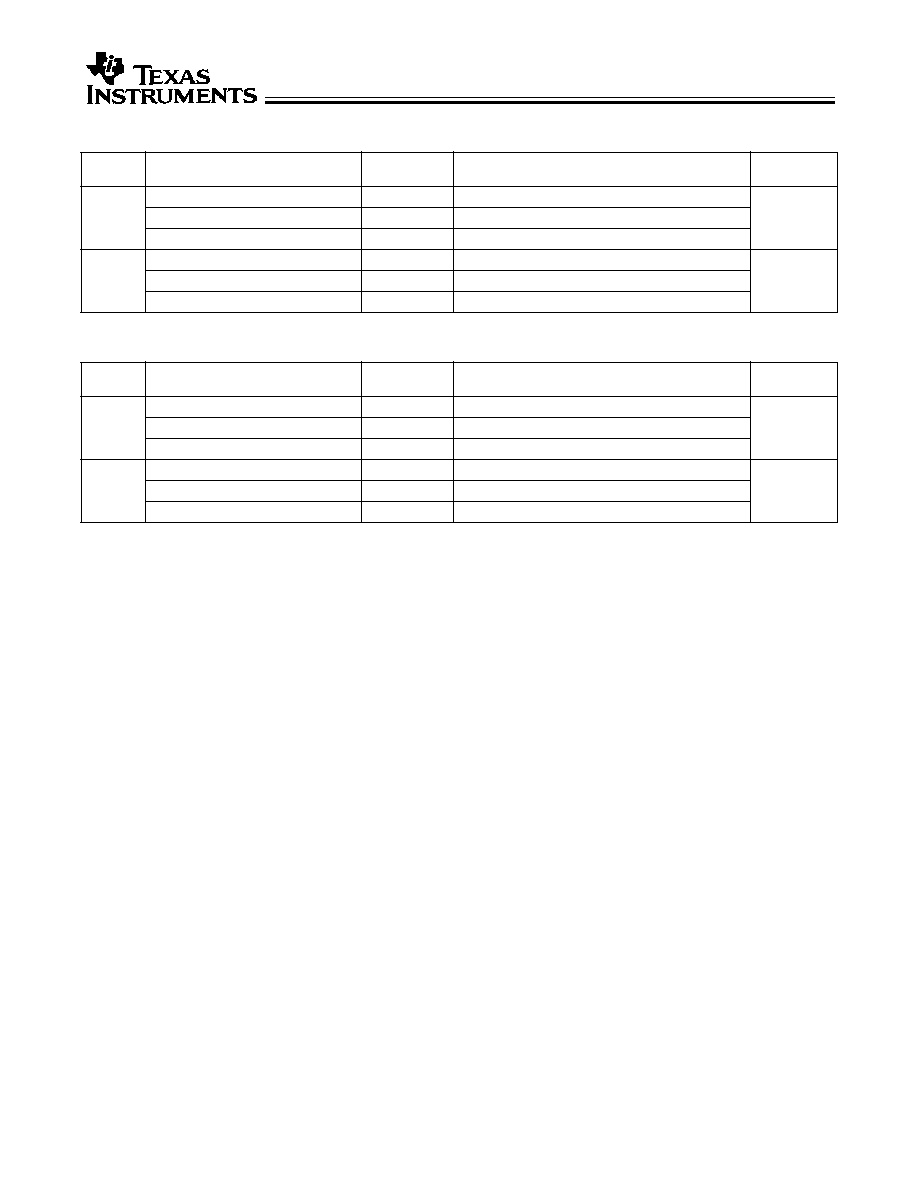
Ordering Information CY74FCT16373
Speed
(ns)
Ordering Code
Package
Name
Package Type
Operating
Range
4.2
CY74FCT16373CTPACT
Z48
48-Lead (240-Mil) TSSOP
Industrial
CY74FCT16373CTPVC/PVCT
O48
48-Lead (300-Mil) SSOP
CY74FCT16373CTVR
-
48-Lead (173-Mil) TVSOP
5.2
CY74FCT16373ATPACT
Z48
48-Lead (240-Mil) TSSOP
Industrial
CY74FCT16373ATPVC/PVCT
O48
48-Lead (300-Mil) SSOP
CY74FCT16373ATVR
-
48-Lead (173-Mil) TVSOP
Ordering Information CY74FCT162373
Speed
(ns)
Ordering Code
Package
Name
Package Type
Operating
Range
4.2
74FCT162373CTPACT
Z48
48-Lead (240-Mil) TSSOP
Industrial
CY74FCT162373CTPVC
O48
48-Lead (300-Mil) SSOP
74FCT162373CTPVCT
O48
48-Lead (300-Mil) SSOP
5.2
74FCT162373ATPACT
Z48
48-Lead (240-Mil) TSSOP
Industrial
CY74FCT162373ATPVC
O48
48-Lead (300-Mil) SSOP
74FCT162373ATPVCT
O48
48-Lead (300-Mil) SSOP