4-Bit Binary Counter
CY54/74FCT163T
SCCS015 - May 1994 - Revised February 2000
Data sheet acquired from Cypress Semiconductor Corporation.
Data sheet modified to remove devices not offered.
Copyright
©
2000, Texas Instruments Incorporated
Features
∑ Function, pinout, and drive compatible with FCT and
F logic
∑ FCT-C speed at 5.8 ns max. (Com'l),
∑ Reduced V
OH
(typically = 3.3V) versions of equivalent
FCT functions
∑ Edge-rate control circuitry for significantly improved
noise characteristics
∑ Power-off disable feature
∑ ESD > 2000V
∑ Matched rise and fall times
∑ Fully compatible with TTL input and output logic levels
∑ Extended commercial range of
-
40∞C to +85∞C
∑ Sink current
64 mA (Com'l),
32 mA (Mil)
Source current
32 mA (Com'l),
12 mA (Mil)
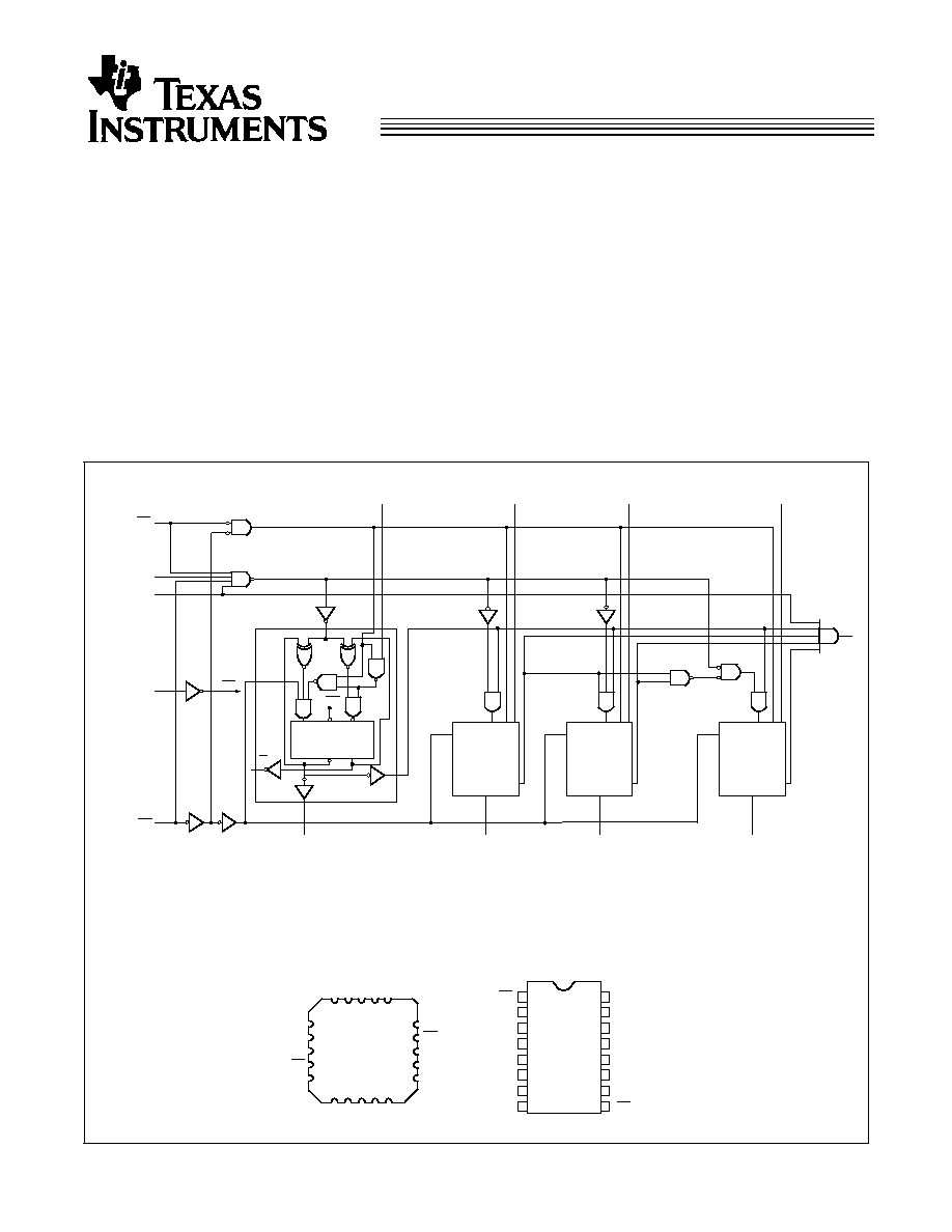
Functional Description
The FCT163T is a high-speed synchronous modulo-16 binary
counter. It is synchronously presettable for application in pro-
grammable dividers and has two types of count enable inputs
plus a terminal count output for versatility in forming synchro-
nous multi-staged counters. The FCT163T has a Synchronous
Reset input that overrides counting and parallel loading and
allows the outputs to be simultaneously reset on the rising
edge of the clock.
The outputs are designed with a power-off disable feature to
allow for live insertion of boards.
Logic Block Diagram
Pin Configurations
Detail A
Q
1
P
0
Detail A
Q
2
Detail A
Q
3
D
Q
CP
D
Q
Q
0
P
1
P
2
P
3
TC
CEP
CP
Q
0
Q
0
Detail A
CP
PE
CET
CP
SR
4
8
9
10
11
12
7
6 5
1516 17 18
3
2
1
20
13
14
19
P
3
CET
PE
NC
CP
NC
NC
V
CC
TC
CEP
GND
SR
Top View
P
0
LCC
NC
P
2
P
1
Q
3
Q
0
Q
2
Q
1
1
2
3
4
5
6
7
8
CP
P
0
P
1
P
3
CEP
V
CC
GND
Top View
SOIC/QSOP
16
15
14
13
12
11
10
9
SR
Q3
CET
PE
TC
Q
0
Q
1
Q
2
P
2
CY54/74FCT163T
2
Maximum Ratings
[2,3]
(Above which the useful life may be impaired. For user guide-
lines, not tested.)
Storage Temperature
.....................................-
65
∞
C to +150
∞
C
Ambient Temperature with
Power Applied
..................................................-
65
∞
C to +135
∞
C
Supply Voltage to Ground Potential
..................-
0.5V to +7.0V
DC Input Voltage
.................................................-
0.5V to +7.0V
DC Output Voltage
..............................................-
0.5V to +7.0V
DC Output Current (Maximum Sink Current/Pin) ...... 120 mA
Power Dissipation .......................................................... 0.5W
Static Discharge Voltage............................................>2001V
(per MIL-STD-883, Method 3015)
Function Table
[1]
Inputs
Action on the Rising
Clock Edge(s)
SR
PE
CET
CEP
L
H
H
H
H
X
L
H
H
H
X
X
H
L
X
X
X
H
X
L
Reset (Clear)
Load (P
n
Q
n
)
Count (Incremental)
No Charge (Hold)
No Charge (Hold)
Pin Description
Name
Description
CEP
Count Enable Parallel Input
CET
Count Enable Trickle Input
CP
Clock Pulse Input (Active Rising Edge)
SR
Synchronous Reset Input (Active LOW)
P
Parallel Data Inputs
PE
Parallel Enable Input (Active LOW)
Q
Flip-Flop Outputs
TC
Terminal Count Output
Operating Range
Range
Range
Ambient
Temperature
V
CC
Commercial
All
-
40
∞
C to +85
∞
C
5V
±
5%
Military
[4]
All
-
55
∞
C to +125
∞
C
5V
±
10%
Electrical Characteristics
Over the Operating Range
Parameter
Description
Test Conditions
Min.
Typ.
[5]
Max.
Unit
V
OH
Output HIGH Voltage
V
CC
=Min., I
OH
=
-
32 mA
Com'l
2.0
V
V
CC
=Min., I
OH
=
-
15 mA
Com'l
2.4
3.3
V
V
CC
=Min., I
OH
=
-
12 mA
Mil
2.4
3.3
V
V
OL
Output LOW Voltage
V
CC
=Min., I
OL
=64 mA
Com'l
0.3
0.55
V
V
CC
=Min., I
OL
=32 mA
Mil
0.3
0.55
V
V
IH
Input HIGH Voltage
2.0
V
V
IL
Input LOW Voltage
0.8
V
V
H
Hysteresis
[6]
All inputs
0.2
V
V
IK
Input Clamp Diode Voltage
V
CC
=Min., I
IN
=
-
18 mA
-
0.7
-
1.2
V
I
I
Input HIGH Current
V
CC
=Max., V
IN
=V
CC
5
µ
A
I
IH
Input HIGH Current
V
CC
=Max., V
IN
=2.7V
±
1
µ
A
I
IL
Input LOW Current
V
CC
=Max., V
IN
=0.5V
±
1
µ
A
I
OS
Output Short Circuit Current
[7]
V
CC
=Max., V
OUT
=0.0V
-
60
-
120
-
225
mA
I
OFF
Power-Off Disable
V
CC
=0V, V
OUT
=4.5V
±
1
µ
A
Notes:
1.
H = HIGH Voltage Level. L = LOW Voltage Level. X = Don't Care.
2.
Unless otherwise noted, these limits are over the operating free-air temperature range.
3.
Unused inputs must always be connected to an appropriate logic voltage level, preferably either V
CC
or ground.
4.
T
A
is the "instant on" case temperature.
5.
Typical values are at V
CC
=5.0V, T
A
=+25∞C ambient.
6.
This parameter is specified but not tested.
7.
Not more than one output should be shorted at a time. Duration of short should not exceed one second. The use of high-speed test apparatus and/or sample
and hold techniques are preferable in order to minimize internal chip heating and more accurately reflect operational values. Otherwise prolonged shorting of
a high output may raise the chip temperature well above normal and thereby cause invalid readings in other parametric tests. In any sequence of parameter
tests, I
OS
tests should be performed last.
CY54/74FCT163T
3
Capacitance
[6]
Parameter
Description
Typ.
[5]
Max.
Unit
C
IN
Input Capacitance
5
10
pF
C
OUT
Output Capacitance
9
12
pF
Power Supply Characteristics
Parameter
Description
Test Conditions
Typ.
[5]
Max.
Unit
I
CC
Quiescent Power Supply Current
V
CC
=Max., V
IN
0.2V, V
IN
V
CC
-
0.2V
0.1
0.2
mA
I
CC
Quiescent Power Supply Current
(TTL inputs HIGH)
V
CC
=Max., V
IN
=3.4V,
[8]
f
1
=0, Outputs Open
0.2
2.0
mA
I
CCD
Dynamic Power Supply Current
[9]
V
CC
=Max., One Bit Toggling, Load Mode,
50% Duty Cycle, Outputs Open,
CEP=CET=PE=GND,
SR=V
CC
, V
IN
0.2V or V
IN
V
CC
-
0.2V
0.06
0.12
mA/MHz
I
C
Total Power Supply Current
[10]
V
CC
=Max., f
0
=10 MHz, Load Mode,
50% Duty Cycle, Outputs Open,
One Bit Toggling at f
1
=5 MHz,
CEP=CET=PE=GND,
SR=V
CC
, V
IN
0.2V or V
IN
V
CC
-
0.2V
0.7
1.4
mA
V
CC
=Max., f
0
=10 MHz, Load Mode,
50% Duty Cycle, Outputs Open,
One Bit Toggling at f
1
=5 MHz,
CEP=CET=PE=GND, SR=V
CC
,
V
IN
=3.4V or V
IN
=GND
1.2
3.4
mA
V
CC
=Max., f
0
=10 MHz, Load Mode,
50% Duty Cycle, Outputs Open,
Four Bits Toggling at f
1
=5 MHz,
CEP=CET=PE=GND,
SR=V
CC
, V
IN
0.2V or V
IN
V
CC
-
0.2V
1.6
3.2
[11]
mA
V
CC
=Max., f
0
=10 MHz, Load Mode,
50% Duty Cycle, Outputs Open,
Four Bits Toggling at f
1
=5 MHz,
CEP=CET=PE=GND, SR=V
CC
,
V
IN
=3.4V or V
IN
=GND
2.9
8.2
[11]
mA
Notes:
8.
Per TTL driven input (V
IN
=3.4V); all other inputs at V
CC
or GND.
9.
This parameter is not directly testable, but is derived for use in Total Power Supply calculations.
10. I
C
= I
QUIESCENT
+ I
INPUTS
+ I
DYNAMIC
I
C
= I
CC
+
I
CC
D
H
N
T
+I
CCD
(f
0
/2 + f
1
N
1
)
I
CC
= Quiescent Current with CMOS input levels
I
CC
= Power Supply Current for a TTL HIGH input (V
IN
=3.4V)
D
H
= Duty Cycle for TTL inputs HIGH
N
T
= Number of TTL inputs at D
H
I
CCD
= Dynamic Current caused by an input transition pair (HLH or LHL)
f
0
= Clock frequency for registered devices, otherwise zero
f
1
= Input signal frequency
N
1
= Number of inputs changing at f
1
All currents are in milliamps and all frequencies are in megahertz.
11. Values for these conditions are examples of the I
CC
formula. These limits are specified but not tested.
CY54/74FCT163T
4
Document #: 38
-
00285
-
B
Switching Characteristics
Over the Operating Range
Parameter
Description
CY54FCT163T
CY74FCT163CT
Unit
Fig. No.
[13]
Military
Commercial
Min.
[12]
Max.
Min.
[12]
Max.
t
PLH
t
PHL
Propagation Delay CP to Q
(PE Input HIGH)
2.0
11.5
1.5
5.8
ns
1, 5
t
PLH
t
PHL
Propagation Delay CP to TC
(PE Input LOW)
2.0
10.0
1.5
5.2
ns
1, 5
t
PLH
t
PHL
Propagation Delay CP to TC
2.0
16.5
1.5
7.8
ns
1, 5
t
PLH
t
PHL
Propagation Delay CET to TC
1.5
9.0
1.5
4.4
ns
1, 5
t
S
Set-Up Time, HIGH or LOW P to CP
5.5
3.5
ns
4
t
H
Hold Time, HIGH or LOW P to CP
2.0
1.5
ns
4
t
SU
Set-Up Time HIGH or LOW
PE or SR to CP
13.5
7.6
ns
4
t
H
Hold Time HIGH or LOW
PE or SR to CP
1.5
1.0
ns
4
t
SU
Set-Up Time HIGH or LOW
CEP or CET to CP
13.0
7.6
ns
4
t
H
Hold Time HIGH or LOW
CEP or CET to CP
0
0
ns
4
t
W
Clock Pulse Width (Load)
HIGH or LOW
5.0
4.0
ns
5
t
W
Clock Pulse Width(Count)
HIGH or LOW
8.0
5.0
ns
5
Notes:
12. Minimum limits are specified but not tested on Propagation Delays.
13. See "Parameter Measurement Information" in the General Information section.
Ordering Information
Speed
(ns)
Ordering Code
Package
Name
Package Type
Operating
Range
5.8
CY74FCT163CTQCT
Q1
16-Lead (150-Mil) QSOP
Commercial
CY74FCT163CTSOC/SOCT
S1
16-Lead (300-Mil) Molded SOIC
11.5
CY54FCT163TLMB
L61
20-Square Leadless Chip Carrier
Military
CY54/74FCT163T
5
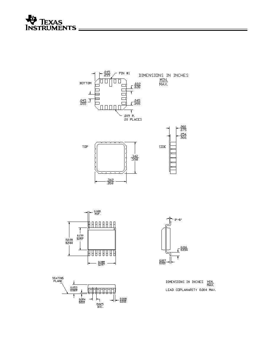
Package Diagrams
20-Pin Square Leadless Chip Carrier L61
MIL
-
STD
-
1835 C
-
2A
16-Lead Quarter Size Outline Q1