
1
Æ
DAC1221
DAC1221
Æ
16-Bit Low Power
DIGITAL-TO-ANALOG CONVERTER
FEATURES
q
16-BIT MONOTONICITY GUARANTEED
OVER ≠40
∞
C TO +85
∞
C
q
LOW POWER: 1.2mW
q
VOLTAGE OUTPUT
q
SETTLING TIME: 2ms to 0.012%
q
MAX LINEARITY ERROR: 30ppm
q
ON-CHIP CALIBRATION
APPLICATIONS
q
PROCESS CONTROL
q
ATE PIN ELECTRONICS
q
CLOSED-LOOP SERVO-CONTROL
q
SMART TRANSMITTERS
q
PORTABLE INSTRUMENTS
q
VCO CONTROL
DESCRIPTION
The DAC1221 is a Digital-to-Analog (D/A) converter
offering 16-bit monotonic performance over the speci-
fied temperature range. It utilizes delta-sigma technol-
ogy to achieve inherently linear performance in a
small package at very low power. The output range is
two times the external reference voltage. On-chip
calibration circuitry dramatically reduces offset and
gain errors.
The DAC1221 features a synchronous serial interface.
In single converter applications, the serial interface can
be accomplished with just two wires, allowing low-
cost isolation. For multiple converters, a CS signal
allows for selection of the appropriate D/A converter.
The DAC1221 has been designed for closed-loop
control applications in the industrial process control
market, and high resolution applications in the test and
measurement market. It is also ideal for remote appli-
cations, battery-powered instruments, and isolated sys-
tems. The DAC1221 is available in a SSOP-16 package.
© 1999 Burr-Brown Corporation
PDS-1519B
Printed in U.S.A. May, 2000
International Airport Industrial Park ∑ Mailing Address: PO Box 11400, Tucson, AZ 85734 ∑ Street Address: 6730 S. Tucson Blvd., Tucson, AZ 85706 ∑ Tel: (520) 746-1111
Twx: 910-952-1111 ∑ Internet: http://www.burr-brown.com/ ∑ Cable: BBRCORP ∑ Telex: 066-6491 ∑ FAX: (520) 889-1510 ∑ Immediate Product Info: (800) 548-6132
DAC1221
For most current data sheet and other product
information, visit www.burr-brown.com
Clock Generator
Serial
Interface
Second-Order
Modulator
Instruction Register
Command Register
Data Register
Offset Register
Full-Scale Register
Microcontroller
First-Order
Switched
Capacitor Filter
Second-Order
Continuous
Time Post Filter
Modulator Control
C
2A
C
2B
C
3
C
1
X
IN
X
OUT
V
REF
CS
DV
DD
DGND
AV
DD
AGND
SDIO
V
OUT
SCLK
SBAS113

2
Æ
DAC1221
SPECIFICATIONS
All specifications T
MIN
to T
MAX
, AV
DD
= DV
DD
= +3V, f
XIN
= 2.5MHz, V
REF
= +1.25V, C
1
= 2.2nF, C
2
= 150pF, C
3
= 6.8nF, unless otherwise noted.
DAC1221E
PARAMETER
CONDITIONS
MIN
TYP
MAX
UNITS
ACCURACY
Monotonicity
16
Bits
Linearity Error
(1)
±
30
ppm of FSR
Offset Error
(2)
V
OUT
= 20mV, CALPIN = 1
(6)
±
190
µ
V
Offset Error Drift
(3)
50
µ
V/
∞
C
Midscale Error
(2)
V
OUT
= V
REF
, CALPIN = 1
(6)
±
20
µ
V
Midscale Error Drift
(3)
50
µ
V/
∞
C
Gain Error
(2)
CALPIN = 1
(6)
0.015
%
Gain Error Drift
(3)
3
ppm/
∞
C
Power-Supply Rejection Ratio
at DC, dB = ≠20log(
V
OUT
/
V
DD
)
57
dB
ANALOG OUTPUT
Output Voltage
(4)
0
2 ∑ V
REF
V
Output Current
(1)
±
0.25
mA
Capacitive Load
500
pF
Short-Circuit Current
±
10
mA
Short-Circuit Duration
GND or V
DD
Indefinite
DYNAMIC PERFORMANCE
Settling Time
(1,5)
To
±
0.012%
1.8
2
ms
Output-Noise Voltage
1Hz to 2kHz
45
µ
Vrms
REFERENCE INPUT
Input Voltage
1.125
1.25
1.375
V
Input Impedance
1
M
DIGITAL INPUT/OUTPUT
Logic Family
TTL-Compatible CMOS
Logic Levels (all except X
IN
)
V
IH
2.0
DV
DD
+ 0.3
V
V
IL
≠0.3
0.8
V
V
OH
I
OH
= ≠0.8mA
2.4
V
V
OL
I
OL
= 1.6mA
0.4
V
Input-Leakage Current
±
10
µ
A
X
IN
Frequency Range (f
XIN
)
1.0
2.5
MHz
Data Format
User Programmable
Offset Two's Complement
or Straight Binary
POWER SUPPLY REQUIREMENTS
Power-Supply Voltage
2.7
3.3
V
Supply Current
Analog Current
320
µ
A
Digital Current
70
µ
A
Power Dissipation
Normal Mode
1.2
1.6
mW
Sleep Mode
0.25
mW
TEMPERATURE RANGE
Specified Performance
≠40
+85
∞
C
NOTES: (1) Valid from AGND + 20mV to 2 ∑ V
REF
. (2) Applies after calibration. (3) Recalibration can remove these errors. (4) Ideal output voltage. (5) Using external
low-pass filter with 2kHz corner frequency. (6) See Command Register for description of CALPIN.

3
Æ
DAC1221
The information provided herein is believed to be reliable; however, BURR-BROWN assumes no responsibility for inaccuracies or omissions. BURR-BROWN assumes
no responsibility for the use of this information, and all use of such information shall be entirely at the user's own risk. Prices and specifications are subject to change
without notice. No patent rights or licenses to any of the circuits described herein are implied or granted to any third party. BURR-BROWN does not authorize or warrant
any BURR-BROWN product for use in life support devices and/or systems.
ABSOLUTE MAXIMUM RATINGS
(1)
AV
DD
to DV
DD
...................................................................................
±
0.3V
AV
DD
to AGND ........................................................................ ≠0.3V to 4V
DV
DD
to DGND ....................................................................... ≠0.3V to 4V
AGND to DGND ...............................................................................
±
0.3V
V
REF
Voltage to AGND .......................................................... 1.0V to 1.5V
Digital Input Voltage to DGND .............................. ≠0.3V to DV
DD
+ 0.3V
Digital Output Voltage to DGND ........................... ≠0.3V to DV
DD
+ 0.3V
Package Power Dissipation ............................................. (T
JMAX
≠ T
A
) /
JA
Maximum Junction Temperature (T
JMAX
) ..................................... +150
∞
C
Thermal Resistance,
JA
SSOP-16 ............................................................................... 200
∞
C/ W
Lead Temperature (soldering, 10s) ............................................... +300
∞
C
NOTE: (1) Stresses above those listed under "Absolute Maximum Ratings"
may cause permanent damage to the device. Exposure to absolute maximum
conditions for extended periods may affect device reliability.
ELECTROSTATIC
DISCHARGE SENSITIVITY
This integrated circuit can be damaged by ESD. Burr-Brown
recommends that all integrated circuits be handled with
appropriate precautions. Failure to observe proper handling
and installation procedures can cause damage.
ESD damage can range from subtle performance degradation
to complete device failure. Precision integrated circuits may
be more susceptible to damage because very small parametric
changes could cause the device not to meet its published
specifications.
PIN CONFIGURATION
Top View
SSOP
PIN DESCRIPTIONS
PIN
NAME
DESCRIPTION
1
DV
DD
Digital Supply, +3V nominal
2
X
OUT
Digital, System Clock Output
3
X
IN
Digital, System Clock Input
4
DGND
Digital Ground
5
AV
DD
Analog Supply, +3V nominal
6
DNC
Do Not Connect
7
C
3
Analog, Filter Capacitor
8
C
2B
Analog, Filter Capacitor
9
C
1
Analog, Filter Capacitor
10
C
2A
Analog, Filter Capacitor
11
V
OUT
Analog Output Voltage
12
V
REF
Analog, Reference Input
13
AGND
Analog Ground
14
CS
Digital, Chip Select Input
15
SDIO
Digital, Serial Data Input/Output
16
SCLK
Digital, Clock Input for Serial Data Transfer
1
2
3
4
5
6
7
8
DV
DD
X
OUT
X
IN
DGND
AV
DD
DNC
C
3
C
2B
SCLK
SDIO
CS
AGND
V
REF
V
OUT
C
2A
C
1
16
15
14
13
12
11
10
9
DAC1221E
PACKAGE
SPECIFIED
DRAWING
TEMPERATURE
PACKAGE
ORDERING
TRANSPORT
PRODUCT
PACKAGE
NUMBER
RANGE
MARKING
NUMBER
(1)
MEDIA
DAC1221E
SSOP-16
322
≠40
∞
C to +85
∞
C
DAC1221E
DAC1221E
Rails
"
"
"
"
"
DAC1221E/2K5
Tape and Reel
NOTE: (1) Models with a slash (/) are available only in Tape and Reel in the quantities indicated (e.g., /2K5 indicates 2500 devices per reel). Ordering 2500 pieces
of "DAC1221E/2K5" will get a single 2500-piece Tape and Reel.
PACKAGE/ORDERING INFORMATION

4
Æ
DAC1221
TYPICAL PERFORMANCE CURVES
At T
A
= +25
∞
C, AV
DD
= DV
DD
= +3.0V, f
XIN
= 2.5MHz, V
REF
= 1.25V, C
1
= 2.2nF, C
2
= 150pF and C
3
= 6.8nF.
POWER SUPPLY REJECTION RATIO vs FREQUENCY
Frequency (Hz)
10
100
1000
10000
100000
PSRR (dB)
70
60
50
40
30
20
10
0
FULL SCALE OUTPUT SWING
Time (ms)
0
1
2
3
4
Output (V)
3.0
2.5
2.0
1.5
1.0
0.5
0
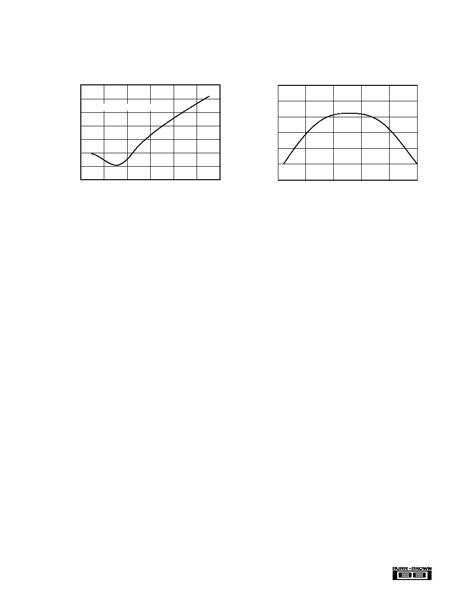
Time (ms)
SETTLING TIME: 20mV to FS
0
2
4
6
8
10
Around FS (
µ
V)
300
0
≠300
≠600
≠900
≠1200
≠1500
SETTLING TIME: FS to 20mV
Time (ms)
0
2
4
6
8
10
Around 20mV (
µ
V)
1500
1200
900
600
300
0
≠300
OFFSET vs TEMPERATURE
Temperature (
∞
C)
≠25
25
75
≠50
0
50
100
Offset (mV)
4
2
0
≠2
≠4
≠6
(can be corrected with calibration)
OUTPUT NOISE VOLTAGE vs FREQUENCY
Frequency (Hz)
10
100
1000
10000
10000
Noise (nv/
Hz)
10000
1000
100
10
1
5
Æ
DAC1221
LINEARITY ERROR vs CODE
16-Bit Input Code Normalized
0
0.2
0.4
0.6
0.8
1
Linearity Error (ppm of FSR)
25
20
15
10
5
0
≠5
GAIN ERROR vs TEMPERATURE
Temperature (
∞
C)
≠50
≠25
0
50
75
25
100
Gain Error (%)
0.020
0.015
0.010
0.005
0.000
≠0.005
≠0.010
≠0.015
(can be corrected with calibration)
TYPICAL PERFORMANCE CURVES
At T
A
= +25
∞
C, AV
DD
= DV
DD
= +3.0V, f
XIN
= 2.5MHz, V
REF
= 1.25V, C
1
= 2.2nF, C
2
= 150pF and C
3
= 6.8nF.