www.ti.com
FEATURES
DESCRIPTION
APPLICATIONS
DAC5571
SLAS405 ≠ DECEMBER 2003
+2.7 V to +5.5 V, I
2
C INTERFACE, VOLTAGE OUTPUT,
8-BIT DIGITAL-TO-ANALOG CONVERTER
∑
Micropower Operation: 125 µA @ 3 V
The DAC5571 is a low-power, single-channel, 8-bit
∑
Fast Update Rate: 188 KSPS
buffered voltage output DAC. Its on-chip precision
output amplifier allows rail-to-rail output swing to be
∑
Power-On Reset to Zero
achieved. The DAC5571 utilizes an I
2
C-compatible,
∑
+2.7-V to +5.5-V Power Supply
two-wire serial interface that operates at clock rates
∑
Specified Monotonic by Design
up to 3.4 Mbps with address support of up to two
∑
I
2
CTM Interface up to 3.4 Mbps
DAC5571s on the same data bus.
∑
On-Chip Output Buffer Amplifier, Rail-to-Rail
The output voltage range of the DAC is 0 V to V
DD
.
Operation
The DAC5571 incorporates a power-on-reset circuit
∑
Double-Buffered Input Register
that ensures that the DAC output powers up at zero
∑
Address Support for up to Two DAC5571s
volts and remains there until a valid write to the
device
takes
place.
The
DAC5571
contains
a
∑
Small 6 Lead SOT 23 Package
power-down feature, accessed via the internal control
∑
Operation From -40
∞
C to 105
∞
C
register, that reduces the current consumption of the
device to 50 nA at 5 V.
The low-power consumption of this part in normal
∑
Process Control
operation makes it ideally suited for portable battery
∑
Data Acquistion Systems
operated equipment. The power consumption is less
∑
Closed-Loop Servo Control
than 0.7 mW at V
DD
= 5 V reducing to 1 µW in
∑
PC Peripherals
power-down mode.
∑
Portable Instrumentation
DAC7571/6571/5571 are 12/10/8-bit, single-channel
I
2
C DACs from the same family. DAC7574/6574/5574
and
DAC7573/6573/5573
are
12/10/8-bit
quad-channel I
2
C DACs. Also see DAC8571/8574 for
single/quad-channel, 16-bit I
2
C DACs.
Please be aware that an important notice concerning availability, standard warranty, and use in critical applications of Texas
Instruments semiconductor products and disclaimers thereto appears at the end of this data sheet.
I
2
C is a trademark of Philips Corporation.
PRODUCTION DATA information is current as of publication date.
Copyright © 2003, Texas Instruments Incorporated
Products conform to specifications per the terms of the Texas
Instruments standard warranty. Production processing does not
necessarily include testing of all parameters.
www.ti.com
V
DD
SCL
A0
GND
Output
Buffer
Power-Down
Control Logic
Resistor
Network
Ref (+) Ref(-)
8-Bit
DAC
I
2
C
Control
Logic
DAC
Register
Power-On
Reset
V
OUT
SDA
PIN CONFIGURATIONS
A0
SCL
SDA
6
5
4
1
2
3
V
OUT
GND
V
DD
D571
1
2
3
6
5
4
YMLL
(TOP VIEW)
(BOTTOM VIEW)
Lot Trace Code
DAC5571
SLAS405 ≠ DECEMBER 2003
This integrated circuit can be damaged by ESD. Texas Instruments recommends that all integrated
circuits be handled with appropriate precautions. Failure to observe proper handling and installation
procedures can cause damage.
ESD damage can range from subtle performance degradation to complete device failure. Precision
integrated circuits may be more susceptible to damage because very small parametric changes could
cause the device not to meet its published specifications.
PACKAGE/ORDERING INFORMATION
PACKAGE
SPECIFIED TEM-
PACKAGE
ORDERING NUM-
PRODUCT
PACKAGE
DESIG-
TRANSPORT MEDIA
PERATURE RANGE
MARKING
BER
NATOR
DAC5571IDBVT
250 Piece Small Tape and Reel
DAC5571
SOT23-6
DBV
-40
∞
C to +105
∞
C
D571
DAC5571IDBVR
3000 Piece Tape and Reel
PIN DESCRIPTION (SOT23-6)
PIN
NAME
DESCRIPTION
1
V
OUT
Analog output voltage from DAC
Ground reference point for all
2
GND
circuitry
3
V
DD
Analog Voltage Supply Input
4
SDA
Serial Data Input
5
SCL
Serial Clock Input
6
A0
Device Address Select
LOT
Year (3 = 2003); M onth (1≠9 = JAN≠SEP; A=OCT,
TRACE
B=NOV, C=DEC); LL≠ Random code generated
CODE:
when assembly is requested
2
www.ti.com
ABSOLUTE MAXIMUM RATINGS
(1)
ELECTRICAL CHARACTERISTICS
DAC5571
SLAS405 ≠ DECEMBER 2003
UNITS
V
DD
to GND
-0.3 V to +6 V
Digital input voltage to GND
-0.3 V to +V
DD
+ 0.3 V
V
OUT
to GND
-0.3 V to +V
DD
+ 0.3 V
Operating temperature range
-40
∞
C to + 105
∞
C
Storage temperature range
-65
∞
C to + 150
∞
C
Junction temperature range (T
J
max)
+ 150
∞
C
Power dissipation
(T
J
max - T
A
)R
JA
Thermal impedance, R
JA
240
∞
C/W
Lead temperature, soldering
Vapor phase (60s)
215
∞
C
Infrared (15s)
220
∞
C
(1)
Stresses above those listed under"Absolute Maximum Ratings" may cause permanent damage to thedevice. Exposure to absolute
maximum conditions for extended periods may affectdevice reliability.
V
DD
= +2.7 V to +5.5 V; R
L
= 2 k
to GND; C
L
= 200 pF to GND; all specifications -40
∞
C to +105
∞
C unless otherwise noted.
DAC5571
PARAMETER
CONDITIONS
UNITS
MIN
TYP
MAX
STATIC PERFORMANCE
(1)
Resolution
8
Bits
Relative accuracy
±
0.5
LSB
Differential nonlinearity
Assured monotonic by design
±
0.25
LSB
Zero code error
All zeroes loaded to DAC register
5
20
mV
Full-scale error
All ones loaded to DAC register
-0.15
-1.25
% of FSR
Gain error
±
1.25
% of FSR
Zero code error drift
±
7
µV/
∞
C
Gain temperature coefficient
±
3
ppm of FSR/
∞
C
OUTPUT CHARACTERISTICS
(2)
Output voltage range
0
V
DD
V
1/4 Scale to 3/4 scale change (400
H
to C00
H
) ;
Output voltage settling time
6
8
µs
R
L
=
Slew rate
1
V/µs
R
L
=
470
pF
Capacitive load stability
R
L
= 2 k
1000
pF
Code change glitch impulse
1 LSB Change around major carry
20
nV-s
Digital feedthrough
0.5
nV-s
DC output impedance
1
V
DD
= +5 V
50
mA
Short-circuit current
V
DD
= +3 V
20
mA
Coming out of power-down mode, V
DD
= +5 V
2.5
µs
Power-up time
Coming out of power-down mode, V
DD
= +3 V
5
µs
LOGIC INPUTS
(2)
Input current
±
1
µA
V
IN
L, Input low voltage
V
DD
= +3 V
0.3
◊
V
DD
V
0.7
◊
V
D
V
IN
H, Input high voltage
V
DD
= +5 V
V
D
Pin capacitance
3
pF
(1)
Linearitycalculated using a reduced code range of 3 to 253; output unloaded.
(2)
Specified by design and characterization, notproduction tested.
3
www.ti.com
TIMING CHARACTERISTICS
DAC5571
SLAS405 ≠ DECEMBER 2003
ELECTRICAL CHARACTERISTICS (continued)
V
DD
= +2.7 V to +5.5 V; R
L
= 2 k
to GND; C
L
= 200 pF to GND; all specifications -40
∞
C to +105
∞
C unless otherwise noted.
DAC5571
PARAMETER
CONDITIONS
UNITS
MIN
TYP
MAX
POWER REQUIREMENTS
V
DD
2.7
5.5
V
I
DD
(normal operation)
DAC active and excluding load current
V
DD
= +3.6 V to +5.5 V
V
IH
= V
DD
and V
IL
= GND
155
200
µA
V
DD
= +2.7 V to +3.6 V
V
IH
= V
DD
and V
IL
= GND
125
160
µA
I
DD
(all power-down modes)
V
DD
= +3.6 V to +5.5 V
V
IH
= V
DD
and V
IL
= GND
0.2
1
µA
V
DD
= +2.7 V to +3.6 V
V
IH
= V
DD
and V
IL
= GND
0.05
1
µA
POWER EFFICIENCY
I
OUT
/I
DD
I
LOAD
= 2 mA, V
DD
= +5 V
93
%
SYMBOL
PARAMETER
TEST CONDITIONS
MIN
TYP
MAX
UNITS
Standard mode
100
kHz
Fast mode
400
kHz
f
SCL
SCL Clock Frequency
High-speed mode, C
B
- 100 pF max
3.4
MHz
High-Speed mode, C
B
- 400 pF max
1.7
MHz
Standard mode
4.7
µs
Bus Free Time Between a STOP
t
BUF
and START Condition
Fast mode
1.3
µs
Standard mode
4.0
µs
Hold Time (Repeated) START
t
HD
; t
STA
Fast mode
600
ns
Condition
High-speed mode
160
ns
Standard mode
4.7
µs
Fast mode
1.3
µs
t
LOW
LOW Period of the SCL Clock
High-speed mode, C
B
- 100 pF max
160
ns
High-speed mode, C
B
- 400 pF max
320
ns
Standard mode
4.0
µs
Fast mode
600
ns
t
HIGH
HIGH Period of the SCL Clock
High-speed mode, C
B
- 100 pF max
60
ns
High-speed mode, C
B
- 400 pF max
120
ns
Standard mode
4.7
µs
Setup Time for a Repeated
t
SU
; t
STA
Fast mode
600
ns
START Condition
High-speed mode
160
ns
Standard mode
250
ns
t
SU
; t
DAT
Data Setup Time
Fast mode
100
ns
High-speed mode
10
ns
Standard mode
0
3.45
µs
Fast mode
0
0.9
µs
t
HD
; t
DAT
Data Hold Time
High-speed mode, C
B
- 100 pF max
0
70
ns
High-speed mode, C
B
- 400 pF max
0
150
ns
Standard mode
20
◊
0.1C
B
1000
ns
Fast mode
20
◊
0.1C
B
300
ns
t
RCL
Rise Time of SCL Signal
High-speed mode, C
B
- 100 pF max
10
40
ns
High-speed mode, C
B
- 400 pF max
20
80
ns
4
www.ti.com
DAC5571
SLAS405 ≠ DECEMBER 2003
TIMING CHARACTERISTICS (continued)
SYMBOL
PARAMETER
TEST CONDITIONS
MIN
TYP
MAX
UNITS
Standard mode
20
◊
0.1C
B
1000
ns
Rise Time of SCL Signal After a
Fast mode
20
◊
0.1C
B
300
ns
t
RCL1
Repeated START Condition and
High-speed mode, C
B
- 100 pF max
10
80
ns
After an Acknowledge BIT
High-speed mode, C
B
- 400 pF max
20
160
ns
Standard mode
20
◊
0.1C
B
300
ns
Fast mode
20
◊
0.1C
B
300
ns
t
FCL
Fall Time of SCL Signal
High-speed mode, C
B
- 100 pF max
10
40
ns
High-speed mode, C
B
- 400 pF max
20
80
ns
Standard mode
20
◊
0.1C
B
1000
ns
Fast mode
20
◊
0.1C
B
300
ns
t
RDA
Rise Time of SDA Signal
High-speed mode, C
B
- 100 pF max
10
80
ns
High-speed mode, C
B
- 400 pF max
20
160
ns
Standard mode
20
◊
0.1C
B
300
ns
Fast mode
20
◊
0.1C
B
300
ns
t
FDA
Fall Time of SDA Signal
High-speed mode, C
B
- 100 pF max
10
80
ns
High-speed mode, C
B
- 400 pF max
20
160
ns
Standard mode
4.0
µs
t
SU
; t
STO
Setup Time for STOP Condition
Fast mode
600
ns
High-speed mode
160
ns
C
B
Capacitive Load for SDA and SCL
400
pF
Fast mode
50
ns
t
SP
Pulse Width of Spike Suppressed
High-speed mode
10
ns
Standard mode
Noise Margin at the HIGH Level
V
NH
for Each Connected Device
Fast mode
0.2V
DD
V
(Including Hysteresis)
High-speed mode
Standard mode
Noise Margin at the LOW Level for
V
NL
Each Connected Device
Fast mode
0.1V
DD
V
(Including Hysteresis)
High-speed mode
5
www.ti.com
TYPICAL CHARACTERISTICS: V
DD
= +5 V
-0.5
-0.4
-0.3
-0.2
-0.1
0
0.1
0.2
0.3
0.4
0.5
-0.25
-0.2
-0.15
-0.1
-0.05
0
0.05
0.1
0.15
0.2
0.25
0
32
64
96
128
160
192
224
256
Digital Input Code
V
DD
= 5 V at 25
∞
C
LE - LSB
DLE - LSB
-0.5
-0.4
-0.3
-0.2
-0.1
0
0.1
0.2
0.3
0.4
0.5
-0.25
-0.2
-0.15
-0.1
-0.05
0
0.05
0.1
0.15
0.2
0.25
0
32
64
96
128
160
192
224
256
V
DD
= 5 V at -40
∞
C
Digital Input Code
LE - LSB
DLE - LSB
-0.5
-0.4
-0.3
-0.2
-0.1
0
0.1
0.2
0.3
0.4
0.5
-0.25
-0.2
-0.15
-0.1
-0.05
0
0.05
0.1
0.15
0.2
0.25
0
32
64
96
128
160
192
224
256
Digital Input Code
V
DD
= 5 V at 105
∞
C
LE - LSB
DLE - LSB
-16
-8
0
8
16
0
32
64
96
128
160
192
224
256
Digital Input Code
V
DD
= 5 V, T
A
= 25
∞
C
Output Error - mV
-30
-20
-10
0
10
20
30
-50 -40 -30 -20 -10 0
10 20 30 40 50 60 70 80 90 100 110
V
DD
= 5 V
T - Temperature -
_
C
Zero-Scale Error
-30
-20
-10
0
10
20
30
-50 -40 -30 -20 -10 0
10 20 30 40 50 60 70 80 90 100 110
V
DD
= 5 V
Full-Scale Error - mV
T - Temperature -
_
C
DAC5571
SLAS405 ≠ DECEMBER 2003
At T
A
= +25
∞
C, +V
DD
= +5 V, unless otherwise noted.
LINEARITY ERROR AND
LINEARITY ERROR AND
DIFFERENTIAL LINEARITY ERROR
DIFFERENTIAL LINEARITY ERROR
vs
vs
CODE (-40
∞
C)
CODE (+25
∞
C )
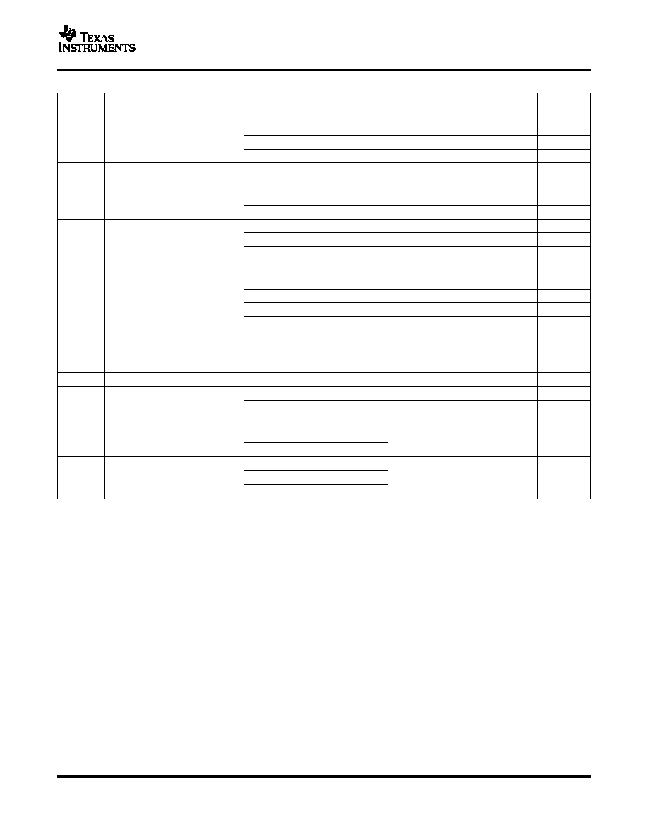
Figure 1.
Figure 2.
LINEARITY ERROR AND
DIFFERENTIAL LINEARITY ERROR
vs
CODE (+105
∞
C)
ABSOLUTE ERROR
Figure 3.
Figure 4.
ZERO-SCALE ERROR
FULL-SCALE ERROR
vs
vs
TEMPERATURE
TEMPERATURE
Figure 5.
Figure 6.
6

www.ti.com
500
1000
1500
2000
2500
80
90
100
1
10
120
130
140
150
160
170
180
190
200
0
V
DD
= 5 V
I
DD
- Supply Current -
m
A
f - Frequency - Hz
0
V
O
U
T
(
V
)
I
SOURCE/SINK
(mA)
5
10
15
5
4
3
2
1
0
DAC Loaded with FF
H
DAC Loaded with 00
H
0
100
200
300
400
500
0
2
32
64
96
128
160
192
224
252
255
Code
V
DD
= 5 V
I DD
A
µ
- Supply Current -
0
50
100
150
200
250
300
-50 -40 -30 -20 -10 0
10 20 30 40 50 60 70 80 90 100 110
V
DD
= 5 V
- Supply Current -
I DD
A
µ
T - Temperature -
_
C
DAC5571
SLAS405 ≠ DECEMBER 2003
TYPICAL CHARACTERISTICS: V
DD
= +5 V (continued)
At T
A
= +25
∞
C, +V
DD
= +5 V, unless otherwise noted.
I
DD
HISTOGRAM
SOURCE AND SINK CURRENT CAPABILITY
Figure 7.
Figure 8.
SUPPLY CURRENT
SUPPLY CURRENT
vs
vs
CODE
TEMPERATURE
Figure 9.
Figure 10.
7
www.ti.com
0
50
100
150
200
250
300
2.7
3.2
3.7
4.2
4.7
5.2
5.7
- Supply Current -
I DD
A
µ
V
DD
- Supply Voltage - V
2.7
I
D
D
(
n
A
)
V
DD
(V)
3.2
3.7
4.2
4.7
5.2
5.7
100
90
80
70
60
50
40
30
20
10
0
+25
∞
C
≠40
∞
C
+105
∞
C
CLK (5V/div)
V
OUT
(1V/div)
Time (1
µ
s/div)
Full-Scale Code Change
00
H
to FF
H
Output Loaded with
2 k
and 200pF to GND
0
I
D
D
(
µ
A
)
V
LOGIC
(V)
1
2
3
4
5
2500
2000
1500
1000
500
0
DAC5571
SLAS405 ≠ DECEMBER 2003
TYPICAL CHARACTERISTICS: V
DD
= +5 V (continued)
At T
A
= +25
∞
C, +V
DD
= +5 V, unless otherwise noted.
SUPPLY CURRENT
POWER-DOWN CURRENT
vs
vs
SUPPLY VOLTAGE
SUPPLY VOLTAGE
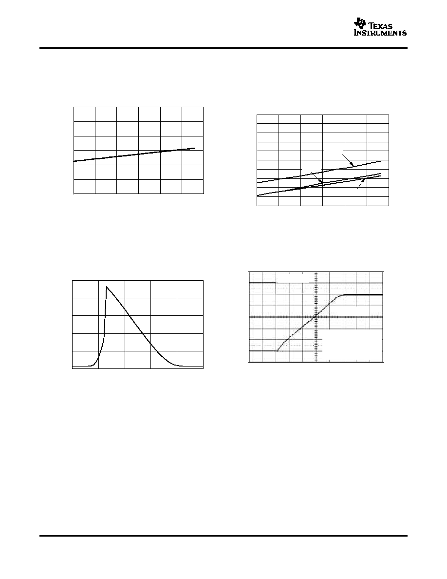
Figure 11.
Figure 12.
SUPPLY CURRENT
vs
LOGIC INPUT VOLTAGE
FULL-SCALE SETTLING TIME
Figure 13.
Figure 14.
8

www.ti.com
Time (1 s/div)
CLK (5V/div)
V
OUT
(1V/div)
Full-Scale Code Change
FF
H
to 00
H
Output Loaded with
2k
and 200pF to GND
µ
Time (1 s/div)
CLK (5V/div)
V
OUT
(1V/div)
Half-Scale Code Change
40
H
to C0
H
Output Loaded with
2 k
and 200 pF to GND
µ
T ime (
s/d iv )
C LK (5 V /div)
V
O U T
(1V /div )
H alf-S ca le C o de C ha nge
C 0
H
to 40
H
O utpu t Lo ad ed w ith
2k
an d 20 0pF to G N D
1m
1
µ
Time (20
µ
s/div)
Loaded with 2k
to V
DD
.
V
DD
(1V/div)
V
OUT
(1V/div)
Tim e (0 .5 s/div )
Loa ded w ith 2 k
and 2 00p F to G N D .
C od e C ha nge :
80
H
t o 7 F
H
V
O
U
T
(
2
0
m
V
/
d
i
v
)
µ
Time (5
µ
s/div)
CLK (5V/div)
V
OUT
(1V/div)
DAC5571
SLAS405 ≠ DECEMBER 2003
TYPICAL CHARACTERISTICS: V
DD
= +5 V (continued)
At T
A
= +25
∞
C, +V
DD
= +5 V, unless otherwise noted.
FULL-SCALE SETTLING TIME
HALF-SCALE SETTLING TIME
Figure 15.
Figure 16.
HALF-SCALE SETTLING TIME
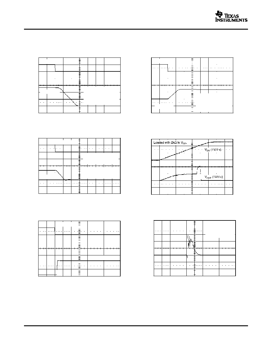
POWER-ON RESET TO 0V
Figure 17.
Figure 18.
EXITING POWER DOWN
(80
H
Loaded)
CODE CHANGE GLITCH
Figure 19.
Figure 20.
9
www.ti.com
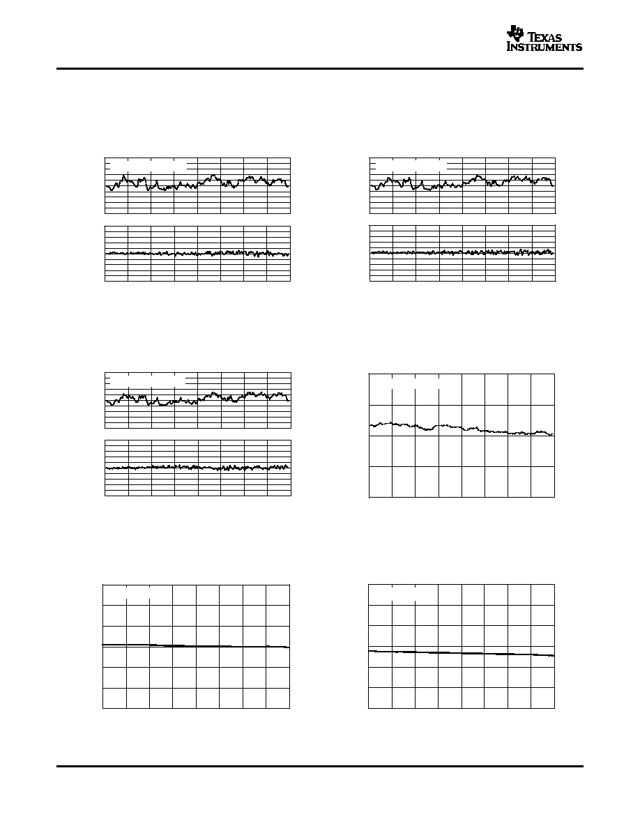
TYPICAL CHARACTERISTICS: V
DD
= +2.7 V
-0.5
-0.4
-0.3
-0.2
-0.1
0
0.1
0.2
0.3
0.4
0.5
-0.25
-0.2
-0.15
-0.1
-0.05
0
0.05
0.1
0.15
0.2
0.25
0
32
64
96
128
160
192
224
256
Digital Input Code
V
DD
= 2.7 V at -40
∞
C
LE - LSB
DLE - LSB
-0.5
-0.4
-0.3
-0.2
-0.1
0
0.1
0.2
0.3
0.4
0.5
-0.25
-0.2
-0.15
-0.1
-0.05
0
0.05
0.1
0.15
0.2
0.25
0
32
64
96
128
160
192
224
256
Digital Input Code
LE - LSB
DLE - LSB
V
DD
= 2.7 V at 25
∞
C
-0.5
-0.4
-0.3
-0.2
-0.1
0
0.1
0.2
0.3
0.4
0.5
-0.25
-0.2
-0.15
-0.1
-0.05
0
0.05
0.1
0.15
0.2
0.25
0
32
64
96
128
160
192
224
256
Digital Input Code
V
DD
= 2.7 V at 105
∞
C
LE - LSB
DLE - LSB
-16
-8
0
8
16
0
32
64
96
128
160
192
224
256
Digital Input Code
Output Error - mV
V
DD
= 2.7 V T
A
= 25
∞
C
-50
-30
-10
10
30
50
70
90
110
-30
-20
-10
0
10
20
30
V
DD
= 5 V
V
DD
= 2.7 V
Full-Scale Error - mV
T - Temperature -
_
C
-30
-20
-10
0
10
20
30
-50
-30
-10
10
30
50
70
90
110
V
DD
= 2.7 V
Zero-ScalenError - mV
T - Temperature -
_
C
DAC5571
SLAS405 ≠ DECEMBER 2003
At T
A
= +25
∞
C, +V
DD
= +2.7 V, unless otherwise noted.
LINEARITY ERROR AND
LINEARITY ERROR AND
DIFFERENTIAL LINEARITY ERROR
DIFFERENTIAL LINEARITY ERROR
vs
vs
CODE (-40
∞
C)
CODE (+25
∞
C)
Figure 21.
Figure 22.
LINEARITY ERROR AND
DIFFERENTIAL LINEARITY ERROR
vs
CODE (+105
∞
C)
ABSOLUTE ERRORS
Figure 23.
Figure 24.
ZERO-SCALE ERROR
FULL-SCALE ERROR
vs
vs
TEMPERATURE
TEMPERATURE
Figure 25.
Figure 26.
10

www.ti.com
0
500
1000
1500
2000
2500
80
90
100
1
10
120
130
140
150
160
170
180
190
200
V
DD
= 2.7 V
I
DD
- Supply Current -
m
A
f - Frequency - Hz
0
V
O
U
T
(
V
)
I
S O U R C E /S IN K
(m A )
5
1 0
1 5
3
2
1
0
D A C Lo ad ed w ith F F
H
D A C Lo ade d w ith 00
H
V
D D
= + 3V
0
100
200
300
400
500
0
2
32
64
96
128
160
192
224
252
255
V
DD
= 2.7 V
Code
I DD
A
µ
- Supply Current -
0
50
100
150
200
250
300
-50
-30
-10
10
30
50
70
90
110
V
DD
= 2.7 V
- Supply Current -
I DD
A
µ
T - Temperature -
_
C
Time (1 s/d iv )
C LK (2.7V /div )
V
O U T
(1V /div )
F ull-S c ale C o de C h an ge
00
H
to F F
H
O utpu t L oad ed w ith
2 k
an d 200 pF to G N D
µ
0
I
D
D
(
µ
A
)
V
LOGIC
(V)
1
2
3
4
5
2500
2000
1500
1000
500
0
DAC5571
SLAS405 ≠ DECEMBER 2003
TYPICAL CHARACTERISTICS: V
DD
= +2.7 V (continued)
At T
A
= +25
∞
C, +V
DD
= +2.7 V, unless otherwise noted.
I
DD
HISTOGRAM
SOURCE AND SINK CURRENT CAPABILITY
Figure 27.
Figure 28.
SUPPLY CURRENT
SUPPLY CURRENT
vs
vs
CODE
TEMPERATURE
Figure 29.
Figure 30.
SUPPLY CURRENT
vs
LOGIC INPUT VOLTAGE
FULL SCALE SETTLING TIME
Figure 31.
Figure 32.
11
www.ti.com
Time (1 s/div)
CLK (2.7V/div)
V
OUT
(1V/div)
Full-Scale Code Change
FF
H
to 00
H
Output Loaded with
2k
and 200pF to GND
µ
Time (1
m
s/div)
CLK (2.7V/div)
V
OUT
(1V/div)
Half-Scale Code Change
40
H
to C0
H
Output Loaded with
2
and 200 pFto GND
k
T im e (1 s/d iv )
C LK (2.7V /div )
V
O U T
(1V /d iv )
H alf-S ca le C ode C ha nge
C 0
H
to 40
H
O u tp ut Lo aded w ith
2k
and 2 00p F to G N D
µ
POWER-ON RESET to 0V
Time (20
µ
s/div)
Tim e (0 .5 s/div )
Loa de d w ith 2k
W
and 2 00pF to G N D .
C ode C hange :
8 0
H
to 7F
H
.
V
O
U
T
(
2
0
m
V
/
d
i
v
)
H
Time (5
µ
s/div)
CLK (2.7V/div)
V
OUT
(1V/div)
DAC5571
SLAS405 ≠ DECEMBER 2003
TYPICAL CHARACTERISTICS: V
DD
= +2.7 V (continued)
At T
A
= +25
∞
C, +V
DD
= +2.7 V, unless otherwise noted.
FULL-SCALE SETTLING TIME
HALF-SCALE SETTLING TIME
Figure 33.
Figure 34.
HALF-SCALE SETTLING TIME
POWER-ON RESET 0 V
Figure 35.
Figure 36.
EXITING-POWER DOWN (80
H
Loaded)
CODE CHANGE GLITCH
Figure 37.
Figure 38.
12
www.ti.com
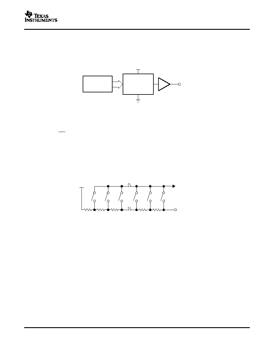
THEORY OF OPERATION
D/A SECTION
REF (+)
REF (-)
Resistor
String
Output
Amplifier
V
OUT
GND
V
DD
DAC Register
V
OUT
+ VDD
D
256
RESISTOR STRING
V
DD
To Output
Amplifier
R
R
R
R
GND
OUTPUT AMPLIFIER
I
2
C Interface
DAC5571
SLAS405 ≠ DECEMBER 2003
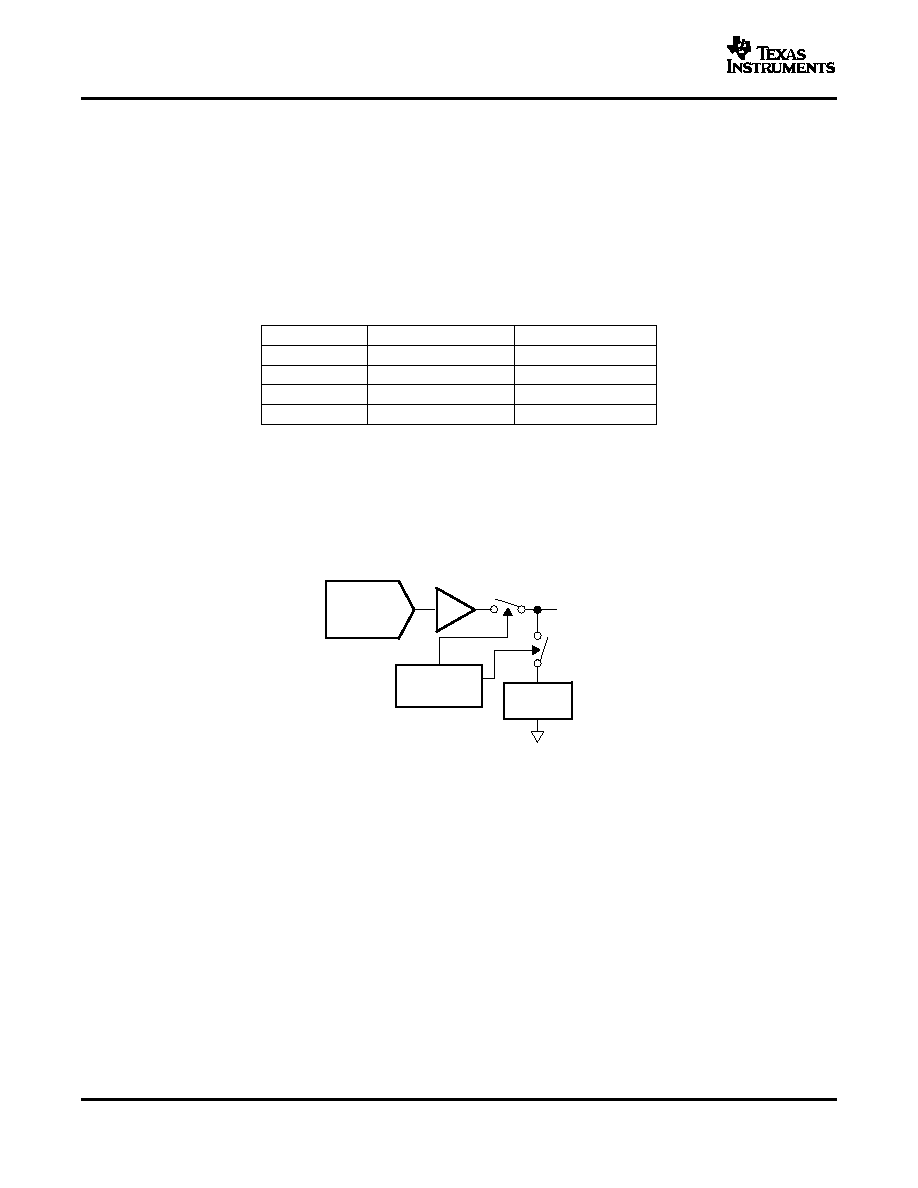
The architecture of the DAC5571 consists of a string DAC followed by an output buffer amplifier. Figure 39
shows a block diagram of the DAC architecture.
Figure 39. R-String DAC Architecture
The input coding to the DAC5571 is unsigned binary, which gives the ideal output voltage as:
where D = decimal equivalent of the binary code that is loaded to the DAC register; it can range from 0 to 255.
The resistor string section is shown in Figure 40. It is basically a divide-by-2 resistor, followed by a string of
resistors, each of value R. The code loaded into the DAC register determines at which node on the string the
voltage is tapped off to be fed into the output amplifier by closing one of the switches connecting the string to the
amplifier. Because the architecture consists of a string of resistors, it is specified monotonic.
Figure 40. Resistor String
The output buffer amplifier is a gain-of-2 amplifier, capable of generating rail-to-rail voltages on its output, which
gives an output range of 0 V to V
DD
. It is capable of driving a load of 2 k
in parallel with 1000 pF to GND. The
source and sink capabilities of the output amplifier can be seen in the typical characteristics curves. The slew
rate is 1 V/µs with a half-scale settling time of 7 µs with the output unloaded.
I
2
C is a two-wire serial interface developed by Philips Semiconductor (see I
2
C-Bus Specification, Version 2.1,
January 2000). The bus consists of a data line (SDA) and a clock line (SCL) with pullup structures. When the bus
is idle, both SDA and SCL lines are pulled high. All the I
2
C compatible devices connect to the I
2
C bus through
open drain I/O pins, SDA and SCL. A master device, usually a microcontroller or a digital signal processor,
controls the bus. The master is responsible for generating the SCL signal and device addresses. The master also
generates specific conditions that indicate the START and STOP of data transfer. A slave device receives and/or
transmits data on the bus under control of the master device.
13
www.ti.com
F/S-Mode Protocol
HS-Mode Protocol
Start
Condition
SDA
Stop
Condition
SDA
SCL
S
P
SCL
DAC5571
SLAS405 ≠ DECEMBER 2003
THEORY OF OPERATION (continued)
The DAC5571 works as a slave and supports the following data transfer modes, as defined in the I
2
C-Bus
Specification: standard mode (100 kbps), fast mode (400 kbps), and high-speed mode (3.4 Mbps). The data
transfer protocol for standard and fast modes is exactly the same; therefore, they are referred to as F/S-mode in
this document. The protocol for high-speed mode is different from the F/S-mode, and it is referred to as
HS-mode. The DAC5571 supports 7-bit addressing; 10-bit addressing and general call address are not
supported.
∑
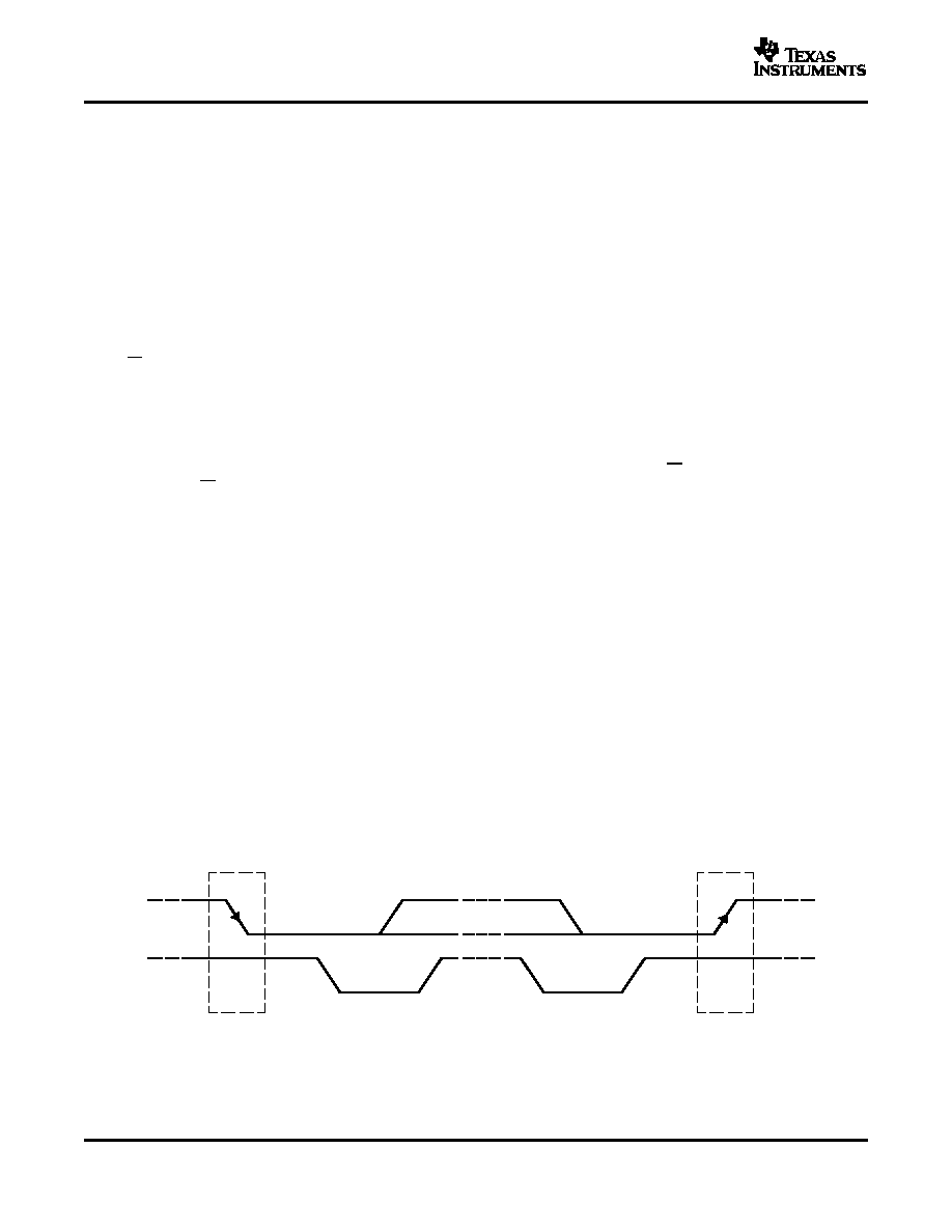
The master initiates data transfer by generating a start condition. The start condition is when a high-to-low
transition occurs on the SDA line while SCL is high, as shown in Figure 41. All I
2
C-compatible devices should
recognize a start condition.
∑
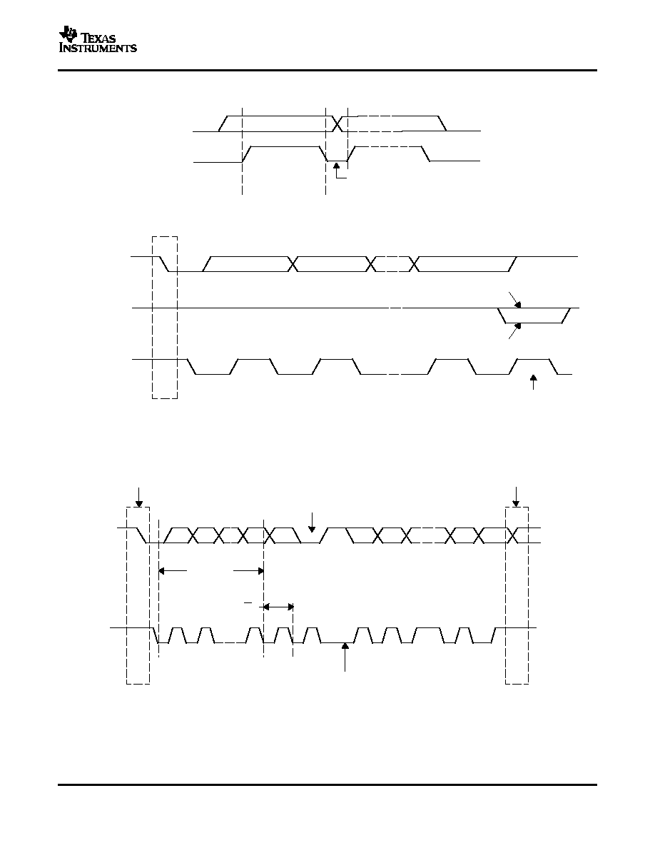
The master then generates the SCL pulses and transmits the 7-bit address and the read/write direction bit
R/W on the SDA line. During all transmissions, the master ensures that data is valid. A valid data condition
requires the SDA line to be stable during the entire high period of the clock pulse (see Figure 42). All devices
recognize the address sent by the master and compare it to their internal fixed addresses. Only the slave
device with a matching address generates an acknowledge (see Figure 43) by pulling the SDA line low
during the entire high period of the ninth SCL cycle. On detecting this acknowledge, the master knows that a
communication link with a slave has been established.
∑
The master generates further SCL cycles to either transmit data to the slave (R/W bit 1) or receive data from
the slave (R/W bit 0). In either case, the receiver needs to acknowledge the data sent by the transmitter. So
an acknowledge signal can either be generated by the master or by the slave, depending on which one is the
receiver. The 9-bit valid data sequences consisting of 8-bit data and 1-bit acknowledge can continue as long
as necessary.
∑
To signal the end of the data transfer, the master generates a stop condition by pulling the SDA line from low
to high while the SCL line is high (see Figure 41). This releases the bus and stops the communication link
with the addressed slave. All I
2
C compatible devices must recognize the stop condition. On the receipt of a
stop condition, all devices know that the bus is released, and they wait for a start condition followed by a
matching address.
∑
When the bus is idle, both SDA and SCL lines are pulled high by the pullup devices.
∑
The master generates a start condition followed by a valid serial byte containing HS master code 00001XXX.
This transmission is made in F/S-mode at no more than 400 Kbps. No device is allowed to acknowledge the
HS master code, but all devices must recognize it and switch their internal setting to support 3.4 Mbps
operation.
∑
The master then generates a repeated start condition (a repeated start condition has the same timing as the
start condition). After this repeated start condition, the protocol is the same as F/S-mode, except that
transmission speeds up to 3.4 Mbps are allowed. A stop condition ends the HS-mode and switches all the
internal settings of the slave devices to support the F/S-mode. Instead of using a stop condition, repeated
start conditions should be used to secure the bus in HS-mode.
Figure 41. START and STOP Conditions
14
www.ti.com
Change of Data Allowed
Data Line
Stable;
Data Valid
SDA
SCL
Not Acknowledge
Acknowledge
1
2
8
9
Clock Pulse for
Acknowledgement
S
START
Condition
Data Output
by Transmitter
Data Output
by Receiver
SCL From
Master
Recognize START or
REPEATED START
Condition
Recognize STOP or
REPEATED START
Condition
Generate ACKNOWLEDGE
Signal
Acknowledgement
Signal From Slave
SDA
SCL
MSB
P
Sr
Sr
or
P
S
or
Sr
START or
Repeated START
Condition
STOP or
Repeated START
Condition
Clock Line Held Low While
Interrupts are Serviced
1
2
7
8
9
ACK
1
2
3 - 8
9
ACK
Address
R/W
DAC5571
SLAS405 ≠ DECEMBER 2003
THEORY OF OPERATION (continued)
Figure 42. Bit Transfer on the I
2
C Bus
Figure 43. Acknowledge on the I
2
C Bus
Figure 44. Bus Protocol
15
www.ti.com
DAC5571 I
2
C Update Sequence
DAC5571
SLAS405 ≠ DECEMBER 2003
THEORY OF OPERATION (continued)
The DAC5571 requires a start condition, a valid I
2
C address, a control-MSB byte, and an LSB byte for a single
update. After the receipt of each byte, DAC5571 acknowledges by pulling the SDA line low during the high period
of a single clock pulse. A valid I
2
C address selects the DAC5571. The CTRL/MSB byte sets the operational
mode of the DAC5571, and the four most significant bits. The DAC5571 then receives the LSB byte containing
four least significant data bits followed by four don't care bits. DAC5571 performs an update on the falling edge
of the acknowledge signal that follows the LSB byte.
For the first update, DAC5571 requires a start condition, a valid I
2
C address, a CTRL/MSB byte, an LSB byte.
For all consecutive updates, DAC5571 needs a CTRL/MSB byte, and an LSB byte.
Using the I
2
C high-speed mode (f
scl
= 3.4 MHz), the clock running at 3.4 MHz, each 8-bit DAC update other than
the first update can be done within 18 clock cycles (CTRL/MSB byte, acknowledge signal, LSB byte,
acknowledge signal), at 188.88 KSPS. Using the fast mode (f
scl
= 400 kHz), clock running at 400 kHz, maximum
DAC update rate is limited to 22.22 KSPS. Once a stop condition is received, DAC5571 releases the I
2
C bus and
awaits a new start condition.
Address Byte
MSB
LSB
1
0
0
1
1
0
A0
0
The address byte is the first byte received following the START condition from the master device. The first six
bits (MSBs) of the address are factory preset to 100110. The next bit of the address is the device select bit A0.
The A0 address input can be connected to V
DD
or digital GND, or can be actively driven by TTL/CMOS logic
levels. The device address is set by the state of this pin during the power-up sequence of the DAC5571. Up to
two devices (DAC5571) can be connected to the same I
2
C-Bus without requiring additional glue logic.
Broadcast Address Byte
MSB
LSB
1
0
0
1
0
0
0
0
Broadcast addressing is also supported by DAC5571. Broadcast addressing can be used for synchronously
updating or powering down multiple DAC5571 devices. Using the broadcast address, DAC5571 responds
regardless of the state of the address pin A0.
Control - Most Significant Byte
Most Significant Byte CTRL/MSB[7:0] consists of two zeros, two power-down bits, and four most significant bits
of 8-bit unsigned binary D/A conversion data.
Least Significant Byte
Least Significant Byte LSB[7:0] consists of the four least significant bits of the 8-bit unsigned binary D/A
conversion data, followed by four don't care bits. DAC5571 updates at the falling edge of the acknowledge signal
that follows the LSB[0] bit.
16
www.ti.com
SLAVE ADDRESS R/W
A
Ctrl/MS-Byte
A
LS-Byte
A/A
P
"0" (write)
Data Transferred
(n* Words + Acknowledge)
Word = 16 Bit
From Master to DAC5571
From DAC5571 to Master
A = Acknowledge (SDA LOW)
A = Not Acknowledge (SDA HIGH)
S = START Condition
Sr = Repeated START Condition
P = STOP Condition
DAC5571 I
2
C-SLAVE ADDRESS:
1
0
0
1
1
0
A0
R/W
MSB
LSB
Factory Preset
A0 = I
2
C Address Pin
Standard- and Fast-Mode:
S
HS-Master Code
R/W
A
Ctrl/MS-Byte
A
LS-Byte
A/A
P
"0" (write)
Data Transferred
(n* Words + Acknowledge)
Word = 16 Bit
High-Speed Mode (HS Mode):
S
A Sr Slave Address
HS Mode Continues
F/S-Mode
HS Mode
F/S Mode
Sr Slave Address
0
0
0
0
1
X
X
R/W
MSB
LSB
HS-Mode Master Code:
0
0
PD1
PD0
D7
D6
D5
D4
MSB
LSB
Ctrl/MS-Byte:
D3
D2
D1
D0
X
X
X
X
MSB
LSB
LS-Byte:
D7 - D0 = Data Bits
'0' = Write to DAC5571
DAC5571
SLAS405 ≠ DECEMBER 2003
Figure 45. Master Transmitter Addressing DAC5571 as a Slave Receiver With a 7-Bit Address
17
www.ti.com
POWER-ON RESET
POWER-DOWN MODES
Resistor
String DAC
Power-Down
V
OUT
Amplifier
Resistor
Network
Circuitry
CURRENT CONSUMPTION
DRIVING RESISTIVE AND CAPACITIVE LOADS
DAC5571
SLAS405 ≠ DECEMBER 2003
The DAC5571 contains a power-on reset circuit that controls the output voltage during power up. On power up,
the DAC register is filled with zeros and the output voltage is 0 V. It remains at a zero-code output until a valid
write sequence is made to the DAC. This is useful in applications where it is important to know the state of the
DAC output while it is in the process of powering up.
The DAC5571 contains four separate modes of operation. These modes are programmable via two bits (PD1
and PD0). Table 1 shows how the state of these bits correspond to the mode of operation.
Table 1. Modes of Operation for the DAC5571
PD1
PD0
OPERATING MODE
0
0
Normal Operation
0
1
1k
to AGND, PWD
1
0
100 k
to AGND, PWD
1
1
High Impedance, PWD
When both bits are set to zero, the device works normally with normal power consumption of 150 µA at 5 V.
However, for the three power-down modes, the supply current falls to 200 nA at 5 V (50 nA at 3 V). Not only
does the supply current fall but the output stage is also internally switched from the output of the amplifier to a
resistor network of known values. This has the advantage that the output impedance of the device is known while
in power-down mode. There are three different options: The output is connected internally to AGND through a
1-k
resistor, a 100-k
resistor, or it is left open-circuited (high impedance). The output stage is illustrated in
Figure 46.
Figure 46. Output Stage During Power Down
All linear circuitry is shut down when the power-down mode is activated. However, the contents of the DAC
register are unaffected when in power down. The time required to exit power down is typically 2.5 µs for AV
DD
=
5 V and 5 µs for AV
DD
= 3 V. See the Typical Characteristics section for more information.
The DAC5571 typically consumes 150 µA at V
DD
= 5 V and 120 µA at V
DD
= 3 V. Additional current consumption
can occur due to the digital inputs if V
IH
<< V
DD
. For most efficient power operation, CMOS logic levels are
recommended at the digital inputs to the DAC. In power-down mode, typical current consumption is 200 nA.
The DAC5571 output stage is capable of driving loads of up to 1000 pF while remaining stable. Within the offset
and gain error margins, the DAC5571 can operate rail-to-rail when driving a capacitive load. When the outputs of
the DAC are driven to the positive rail under resistive loading, the PMOS transistor of each Class-AB output
stage can enter into the linear region. When this occurs, the added IR voltage drop deteriorates the linearity
performance of the DAC. This may occur within approximately the top 20 mV of the DAC's digital input-to-voltage
output transfer characteristic.
18
www.ti.com
OUTPUT VOLTAGE STABILITY
APPLICATIONS
USING REF02 AS A POWER SUPPLY FOR THE DAC5571
REF02
15 V
5 V
1.14 mA
A0
SCL
SDA
I
2
C
Interface
V
OUT
= 0 V to 5 V
DAC5571
LAYOUT
DAC5571
SLAS405 ≠ DECEMBER 2003
The DAC5571 exhibits excellent temperature stability of 5 ppm/
∞
C typical output voltage drift over the specified
temperature range of the device. This enables the output voltage to stay within a
±
25-µV window for a
±
1
∞
C
ambient temperature change. Combined with good dc noise performance and true 8-bit differential linearity, the
DAC5571 becomes a perfect choice for closed-loop control applications.
Due to the extremely low supply current required by the DAC5571, a possible configuration is to use a REF02
+5-V precision voltage reference to supply the required voltage to the DAC5571's supply input as well as the
reference input, as shown in Figure 47. This is especially useful if the power supply is quite noisy or if the system
supply voltages are at some value other than 5 V. The REF02 outputs a steady supply voltage for the DAC5571.
If the REF02 is used, the current it needs to supply to the DAC5571 is 140 µA typical. When a DAC output is
loaded, the REF02 also needs to supply the current to the load. The total typical current required (with a 5-mW
load on a given DAC output) is: 140 µA + (5 mW/5 V) = 1.14 mA.
The load regulation of the REF02 is typically (0.005%
◊
V
DD
)/mA, which results in an error of 0.285 mV for the
1.14-mA current drawn from it. This corresponds to a 0.015 LSB error for a 0-V to 5-V output range.
Figure 47. REF02 as Power Supply to DAC5571
A precision analog component requires careful layout, adequate bypassing, and clean, well-regulated power
supplies.
The power applied to V
DD
should be well regulated and low noise. Switching power supplies and dc/dc
converters often has high-frequency glitches or spikes riding on the output voltage. In addition, digital
components can create similar high-frequency spikes as their internal logic switches states. This noise can easily
couple into the DAC output voltage through various paths between the power connections and analog output.
As with the GND connection, V
DD
should be connected to a +5-V power supply plane or trace that is separate
from the connection for digital logic until they are connected at the power entry point. In addition, the 1-µF to
10-µF and 0.1-µF bypass capacitors are strongly recommended. In some situations, additional bypassing may be
required, such as a 100-µF electrolytic capacitor or even a Pi filter made up of inductors and capacitors--all
designed to essentially low-pass filter the +5-V supply, removing the high-frequency noise.
19

IMPORTANT NOTICE
Texas Instruments Incorporated and its subsidiaries (TI) reserve the right to make corrections, modifications,
enhancements, improvements, and other changes to its products and services at any time and to discontinue
any product or service without notice. Customers should obtain the latest relevant information before placing
orders and should verify that such information is current and complete. All products are sold subject to TI's terms
and conditions of sale supplied at the time of order acknowledgment.
TI warrants performance of its hardware products to the specifications applicable at the time of sale in
accordance with TI's standard warranty. Testing and other quality control techniques are used to the extent TI
deems necessary to support this warranty. Except where mandated by government requirements, testing of all
parameters of each product is not necessarily performed.
TI assumes no liability for applications assistance or customer product design. Customers are responsible for
their products and applications using TI components. To minimize the risks associated with customer products
and applications, customers should provide adequate design and operating safeguards.
TI does not warrant or represent that any license, either express or implied, is granted under any TI patent right,
copyright, mask work right, or other TI intellectual property right relating to any combination, machine, or process
in which TI products or services are used. Information published by TI regarding third-party products or services
does not constitute a license from TI to use such products or services or a warranty or endorsement thereof.
Use of such information may require a license from a third party under the patents or other intellectual property
of the third party, or a license from TI under the patents or other intellectual property of TI.
Reproduction of information in TI data books or data sheets is permissible only if reproduction is without
alteration and is accompanied by all associated warranties, conditions, limitations, and notices. Reproduction
of this information with alteration is an unfair and deceptive business practice. TI is not responsible or liable for
such altered documentation.
Resale of TI products or services with statements different from or beyond the parameters stated by TI for that
product or service voids all express and any implied warranties for the associated TI product or service and
is an unfair and deceptive business practice. TI is not responsible or liable for any such statements.
Following are URLs where you can obtain information on other Texas Instruments products and application
solutions:
Products
Applications
Amplifiers
amplifier.ti.com
Audio
www.ti.com/audio
Data Converters
dataconverter.ti.com
Automotive
www.ti.com/automotive
DSP
dsp.ti.com
Broadband
www.ti.com/broadband
Interface
interface.ti.com
Digital Control
www.ti.com/digitalcontrol
Logic
logic.ti.com
Military
www.ti.com/military
Power Mgmt
power.ti.com
Optical Networking
www.ti.com/opticalnetwork
Microcontrollers
microcontroller.ti.com
Security
www.ti.com/security
Telephony
www.ti.com/telephony
Video & Imaging
www.ti.com/video
Wireless
www.ti.com/wireless
Mailing Address:
Texas Instruments
Post Office Box 655303 Dallas, Texas 75265
Copyright
2004, Texas Instruments Incorporated