www.ti.com
FEATURES
APPLICATIONS
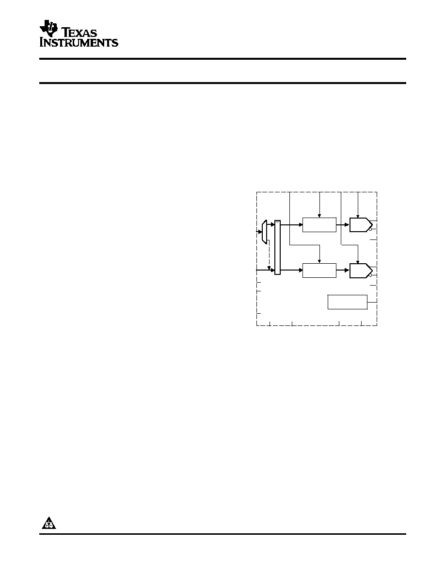
DE
MUX
DA[11:0]
DB[11:0]
MODE
GSET
Latch A
Latch B
12-b DAC
12-b DAC
IOUTA1
IOUTA2
IOUTB1
IOUTB2
1.2 V Reference
WRTB
WRTA
CLKB
CLKA
BIASJ_A
BIASJ_B
EXTIO
DVDD
DGND
AVDD
AGND
SLEEP
DESCRIPTION
DAC5662
SLAS425 ≠ JULY 2004
DUAL, 12-BIT 200 MSPS DIGITAL-TO-ANALOG CONVERTER
∑
Cellular Base Transceiver Station Transmit
∑
12-Bit Dual Transmit DAC
Channel
∑
200 MSPS Update Rate
≠ CDMA: W-CDMA, CDMA2000, IS-95
∑
Single Supply: 3.0 V - 3.6 V
≠ TDMA: GSM, IS-136, EDGE/UWC-136
∑
High SFDR: 85 dBc at 5 MHz
∑
Medical/Test Instrumentation
∑
High IMD3: 78 dBc at 15.1 and 16.1 MHz
∑
Arbitrary Waveform Generators (ARB)
∑
WCDMA ACLR: 70 dB at 30.72 MHz
∑
Direct Digital Synthesis (DDS)
∑
Independent or Single Resistor Gain Control
∑
Cable Modem Termination System (CMTS)
∑
Dual or Interleaved Data
∑
On-Chip 1.2-V Reference
∑
Low Power: 330 mW
∑
Power-Down Mode: 15 mW
∑
Package: 48-Pin TQFP
Figure 1.
The DAC5662 is a monolithic, dual-channel 12-bit high-speed digital-to-analog converter (DAC) with on-chip
voltage reference.
Operating with update rates of up to 200 MSPS, the DAC5662 offers exceptional dynamic performance and
tight-gain and offset matching, characteristics that make it suitable in either I/Q baseband or direct IF
communication applications.
Each DAC has a high-impedance differential current output, suitable for single-ended or differential analog-output
configurations. External resistors allow scaling the full-scale output current for each DAC separately or together,
typically between 2 mA and 20 mA. An accurate on-chip voltage reference is temperature compensated and
delivers a stable 1.2-V reference voltage. Optionally, an external reference may be used.
The DAC5662 has two 12-bit parallel input ports with separate clocks and data latches. For flexibility, the
DAC5662 also supports multiplexed data for each DAC on one port when operating in the interleaved mode.
The DAC5662 has been specifically designed for a differential transformer coupled output with a 50-
doubly
terminated load. For a 20-mA full-scale output current a 4:1 impedance ratio (resulting in an output power of
4 dBm) and 1:1 impedance ratio transformer (-2 dBm output power) are supported.
Please be aware that an important notice concerning availability, standard warranty, and use in critical applications of Texas
Instruments semiconductor products and disclaimers thereto appears at the end of this data sheet.
PRODUCTION DATA information is current as of publication date.
Copyright © 2004, Texas Instruments Incorporated
Products conform to specifications per the terms of the Texas
Instruments standard warranty. Production processing does not
necessarily include testing of all parameters.

www.ti.com
DEVICE INFORMATION
13 14 15
NC
NC
DB0 (LSB)
DB1
DB2
DB3
DB4
DB5
DB6
DB7
DB8
DB9
36
35
34
33
32
31
30
29
28
27
26
25
16
1
2
3
4
5
6
7
8
9
10
11
12
DA11 (MSB)
DA10
DA9
DA8
DA7
DA6
DA5
DA4
DA3
DA2
DA1
DA0 (LSB)
17 18 19 20
AGND
47 46 45 44 43
48
42
IOUT
A1
IOUT
A2
BIASJ_A
EXTIO
GSET
BIASJ_B
IOUTB2
DVDD
DB1
1 (MSB)
DB10
DGND
DVDD
WR
T
A/WR
TIQ
CLKA/CLKIQ
CLKB/RESETIQ
WR
TB/SELECTIQ
DGND
40 39 38
41
21 22 23 24
37
NC
SLEEP
IOUTB1
MODE
A
VDD
NC
Top View
48-Pin TQFP
PFB Package
DAC5662
SLAS425 ≠ JULY 2004
The DAC5662 is available in a 48-pin thin quad FlatPack (TQFP). Pin compatibility between family members
provides 12-bit (DAC5662) and 14-bit (DAC5672) resolution. Furthermore, the DAC5662 is pin compatible to the
DAC2902 and AD9765 dual DACs. The device is characterized for operation over the industrial temperature
range of -40
∞
C to 85
∞
C.
AVAILABLE OPTIONS
T
A
PACKAGED DEVICES
48-TQFP
-40
∞
C to 85
∞
C
DAC5662IPFB
DAC5662IPFBR
TERMINAL FUNCTIONS
TERMINAL
I/O
DESCRIPTION
NAME
NO.
AGND
38
I
Analog ground
AVDD
47
I
Analog supply voltage
BIASJ_A
44
O
Full-scale output current bias for DACA
BIASJ_B
41
O
Full-scale output current bias for DACB
CLKA/CLKIQ
18
I
Clock input for DACA, CLKIQ in interleaved mode.
CLKB/RESETI
19
I
Clock input for DACB, RESETIQ in interleaved mode.
Q
DA[11:0]
1-12
I
Data port A. DA11 is MSB and DA0 is LSB.
DB[11:0]
23-34
I
Data port B. DB11 is MSB and DB0 is LSB.
DGND
15, 21
I
Digital ground
DVDD
16, 22
I
Digital supply voltage
EXTIO
43
I/O
Internal reference output (bypass with 0.1
µ
F to AGND) or external reference input.
2
www.ti.com
DAC5662
SLAS425 ≠ JULY 2004
DEVICE INFORMATION (continued)
TERMINAL FUNCTIONS (continued)
TERMINAL
I/O
DESCRIPTION
NAME
NO.
GSET
42
I
Gain-setting mode: H - 1 resistor, L - 2 resistors. Internal pullup.
IOUTA1
46
O
DACA current output. Full-scale with all bits of DA high.
IOUTA2
45
O
DACA complementary current output. Full-scale with all bits of DA low.
IOUTB1
39
O
DACB current output. Full-scale with all bits of DB high.
IOUTB2
40
O
DACB complementary current output. Full-scale with all bits of DB low.
MODE
48
I
Mode Select: H ≠ Dual Bus, L ≠ Interleaved. Internal pullup.
13, 14, 35,
NC
-
No connection
36
Sleep function control input: H ≠ DAC in power-down mode, L ≠ DAC in operating mode. Internal
SLEEP
37
I
pulldown.
WRTA/WRTIQ
17
I
Input write signal for PORT A (WRTIQ in interleaving mode).
WRTB/SELEC
20
I
Input write signal for PORT B (SELECTIQ in interleaving mode).
TIQ
3
www.ti.com
ABSOLUTE MAXIMUM RATINGS
ELECTRICAL CHARACTERISTICS
DAC5662
SLAS425 ≠ JULY 2004
over operating free-air temperature range (unless otherwise noted)
(1)
UNIT
Supply voltage range
AVDD
(2)
-0.5 V to 4 V
DVDD
(3)
-0.5 V to 4 V
Voltage between AGND and DGND
-0.5 V to 0.5 V
Voltage between AVDD and DVDD
-0.5 V to 0.5 V
Supply voltage range
DA[11:0] and DB[11:0]
(3)
-0.5 V to DVDD + 0.5 V
MODE, CLKA, CLKB, WRTA, WRTB
(3)
-0.5 V to DVDD + 0.5 V
IOUTA1, IOUTA2, IOUTB1, IOUTB2
(2)
-1.0 V to AVDD + 0.5 V
EXTIO, BIASJ_A, BIASJ_B, SLEEP
(2)
-0.5 V to AVDD + 0.5 V
Peak input current (any input)
+20 mA
Peak total input current (all inputs)
-30 mA
Operating free-air temperature range
-40
∞
C to 85
∞
C
Storage temperature range
-65
∞
C to 150
∞
C
Lead temperature 1,6 mm (1/16 inch) from the case for 10
260
∞
C
seconds
(1)
Stresses beyond those listed under "absolute maximum ratings" may cause permanent damage to the device. These are stress ratings
only and functional operation of these or any other conditions beyond those indicated under "recommended operating conditions" is not
implied. Exposure to absolute-maximum-rated conditions for extended periods may affect device reliability.
(2)
Measured with respect to AGND.
(3)
Measured with respect to DGND.
over operating free-air temperature range, AVDD = DVDD = 3.3 V, IOUTFS = 20 mA, independent gain set mode (unless
otherwise noted)
PARAMETER
TEST CONDITIONS
MIN
TYP
MAX
UNIT
DC Specifications
Resolution
12
Bits
DC Accuracy
(1)
INL
Integral nonlinearity
1 LSB = IOUT
FS
/2
12
, T
A
= 25
∞
C
-2
±
0.3
2
LSB
DNL
Differential nonlinearity
-2
±
0.2
2
LSB
Analog Output
Offset error
0.03
%FSR
Gain error
With external reference
±
0.25
%FSR
With internal reference
±
0.5
%FSR
Minimum full-scale output current
(2)
2
mA
Maximum full-scale output current
(2)
20
mA
Gain mismatch
With internal reference
-2
0.07
+2
%FSR
Output voltage compliance range
(3)
-1
1.25
V
R
O
Output resistance
300
k
C
O
Output capacitance
5
pF
Reference Output
Reference voltage
1.14
1.2
1.26
V
Reference output current
(4)
100
nA
(1)
Measured differentially through 50
to AGND.
(2)
Nominal full-scale current, IOUTFS, equals 32x the IBIAS current.
(3)
The lower limit of the output compliance is determined by the CMOS process. Exceeding this limit may result in transistor breakdown,
resulting in reduced reliability of the DAC5662 device. The upper limit of the output compliance is determined by the load resistors and
full-scale output current. Exceeding the upper limit adversely affects distortion performance and intergral nonlinearity.
(4)
Use an external buffer amplifier with high impedance input to drive any external load.
4

www.ti.com
ELECTRICAL CHARACTERISTICS
DAC5662
SLAS425 ≠ JULY 2004
ELECTRICAL CHARACTERISTICS (continued)
over operating free-air temperature range, AVDD = DVDD = 3.3 V, IOUTFS = 20 mA, independent gain set mode (unless
otherwise noted)
PARAMETER
TEST CONDITIONS
MIN
TYP
MAX
UNIT
Reference Input
V
EXTIO
Input voltage
0.1
1.25
V
R
I
Input resistance
1
M
Small signal bandwidth
300
kHz
C
I
Input capacitance
100
pF
Temperature Coefficients
Offset drift
0
ppm of
FSR/
∞
C
Gain drift
With external reference
±
50
ppm of
FSR/
∞
C
With internal reference
±
50
ppm of
FSR/
∞
C
Reference voltage drift
±
20
ppm/
∞
C
over operating free-air temperature range, AVDD = DVDD = 3.3 V, IOUTFS = 20 mA, f
DATA
= 200 MSPS, f
OUT
= 1 MHz,
independent gain set mode (unless otherwise noted)
PARAMETER
TEST CONDITIONS
MIN
TYP
MAX
UNIT
Power Supply
AVDD
Analog supply voltage
3
3.3
3.6
V
DVDD
Digital supply voltage
3
3.3
3.6
V
I
AVDD
Supply current, analog
Including output current through load
75
90
mA
resistor
Sleep mode with clock
2.5
6
mA
Sleep mode without clock
2.5
mA
I
DVDD
Supply current, digital
25
38
mA
Sleep mode with clock
12.5
18
mA
Sleep mode without clock
<10
µA
Power dissipation
330
390
mW
Sleep mode without clock
15
mW
APSSR
Power supply rejection ratio
-0.2
0.2
%FSR/V
DPSRR
-0.2
0.2
%FSR/V
T
A
Operating free-air temperature
-40
85
∞
C
5
www.ti.com
ELECTRICAL CHARACTERISTICS
DAC5662
SLAS425 ≠ JULY 2004
AC specifications over operating free-air temperature range, AVDD = DVDD = 3.3 V, IOUTFS = 20 mA, independent gain set
mode, differential 1:1 impedance ratio transformer coupled output, 50-
doubly terminated load (unless otherwise noted)
PARAMETER
TEST CONDITIONS
MIN
TYP
MAX
UNIT
Analog Output
f
clk
Maximum output update rate
200
MSPS
t
s
Output settling time to 0.1% (DAC)
Mid-scale transition
20
ns
t
r
Output rise time 10% to 90% (OUT)
1.4
ns
t
f
Output fall time 90% to 10% (OUT)
1.5
ns
Output noise
IOUT
FS
= 20 mA
55
pA/
Hz
IOUT
FS
= 2 mA
30
pA/
Hz
AC Linearity
SFDR
Spurious free dynamic range
1st Nyquist zone, T
A
= 25
∞
C, f
DATA
=
81
dBc
50 MSPS, f
OUT
= 1 MHz, IOUTFS =
0 dB
1st Nyquist zone, T
A
= 25
∞
C, f
DATA
=
83
dBc
50 MSPS, f
OUT
= 1 MHz, IOUTFS =
-6 dB
1st Nyquist zone, T
A
= 25
∞
C, f
DATA
=
81
dBc
50 MSPS, f
OUT
= 1 MHz, IOUTFS =
-12 dB
1st Nyquist zone, T
A
= 25
∞
C, f
DATA
=
85
dBc
100 MSPS, f
OUT
= 5 MHz
1st Nyquist zone, T
A
= 25
∞
C, f
DATA
=
78
dBc
100 MSPS, f
OUT
= 20 MHz
1st Nyquist zone, T
MIN
to T
MAX
,
66
71
dBc
f
DATA
= 200 MSPS, f
OUT
= 20 MHz
1st Nyquist zone, T
A
= 25
∞
C, f
DATA
=
68
dBc
200 MSPS, f
OUT
= 41 MHz
SNR
Signal-to-noise ratio
1st Nyquist zone, T
A
= 25
∞
C, f
DATA
=
73
dB
100 MSPS, f
OUT
= 5 MHz
1st Nyquist zone, T
A
= 25
∞
C, f
DATA
=
67
dB
200 MSPS, f
OUT
= 20 MHz
ACLR
Adjacent channel leakage ratio
W-CDMA signal with 3.84-MHz
70
dB
Bandwidth, f
DATA
= 61.44 MSPS, IF
= 15.360 MHz
W-CDMA signal with 3.84-MHz
70
dB
Bandwidth, f
DATA
= 122.88 MSPS, IF
= 30.72 MHz
IMD3
Third-order two-tone intermodulation
Each tone at -6 dBFS, T
A
= 25
∞
C,
62
dBc
f
DATA
= 200 MSPS, f
OUT
= 45.4 and
46.4 MHz
Each tone at -6 dBFS, T
A
= 25
∞
C,
78
dBc
f
DATA
= 100 MSPS, f
OUT
= 15.1 and
16.1 MHz
IMD
Four-tone intermodulation
Each tone at -12 dBFS, T
A
= 25
∞
C,
77
dBc
f
DATA
= 100 MSPS, f
OUT
= 15.6,
15.8, 16.2, and 16.4 MHz
Each tone at -12 dBFS, T
A
= 25
∞
C,
56
dBc
f
DATA
= 165 MSPS, f
OUT
= 68.8,
69.6, 71.2, and 72.0 MHz
Each tone at -12 dBFS, T
A
= 25
∞
C,
74
dBc
f
DATA
= 165 MSPS, f
OUT
= 19.0,
19.1, 19.3, and 19.4 MHz
Channel isolation
T
A
= 25
∞
C, f
DATA
= 165 MSPS, f
OUT
97
dBc
(CH1) = 20 MHz, f
OUT
(CH2) = 21
MHz
6

www.ti.com
ELECTRICAL CHARACTERISTICS
SWITCHING CHARACTERISTICS
DAC5662
SLAS425 ≠ JULY 2004
Digital specifications over operating free-air temperature range, AVDD = DVDD = 3.3 V, IOUTFS = 20 mA (unless otherwise
noted)
PARAMETER
TEST CONDITIONS
MIN
TYP
MAX
UNIT
Digital Input
V
IH
High-level input voltage
2
3.3
V
V
IL
Low-level input voltage
0
0.8
V
I
IH
High-level input current
±
50
µA
I
IL
Low-level input current
±
10
µA
I
IH(GSET)
High-level input current, GSET pin
7
µA
I
IL(GSET)
Low-level input current, GSET pin
-30
µA
I
IH(MODE)
High-level input current, MODE pin
-30
µA
I
IL(MODE)
Low-level input current, MODE pin
-80
µA
C
I
Input capacitance
5
pF
Digital specifications over operating free-air temperature range, AVDD = DVDD = 3.3 V, IOUTFS = 20 mA (unless otherwise
noted)
PARAMETER
TEST CONDITIONS
MIN
TYP
MAX
UNIT
Timing - Dual Bus Mode
t
su
Input setup time
1
ns
t
h
Input hold time
1
ns
t
LPH
Input clock pulse high time
2
ns
t
LAT
Clock latency (WRTA/B to outputs)
4
4
clk
t
PD
Propagation delay time
1.5
ns
Timing - Single Bus Interleaved Mode
t
su
Input setup time
0.5
ns
t
h
Input hold time
0.5
ns
t
LAT
Clock latency (WRTA/B to outputs)
4
4
clk
t
PD
Propagation delay time
1.5
ns
7
www.ti.com
TYPICAL CHARACTERISTICS
-0.4
-0.3
-0.2
-0.1
-0.0
0.1
0.2
0.3
0.4
0
512
1024
1536
2048
2560
3072
3584
4096
Input Code
INL - Integral Nonlinearity Error - LSB
G001
-0.20
-0.15
-0.10
-0.05
-0.00
0.05
0.10
0.15
0.20
0
512
1024
1536
2048
2560
3072
3584
4096
Input Code
DNL - Differential Nonlinearity Error - LSB
G002
DAC5662
SLAS425 ≠ JULY 2004
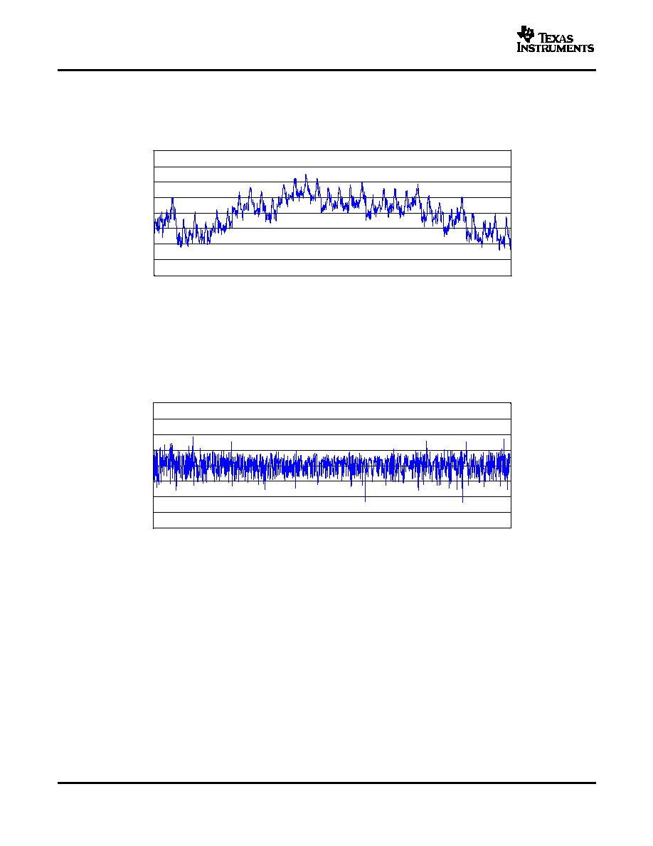
INTEGRAL NONLINEARITY
vs
INPUT CODE
Figure 2.
DIFFERENTIAL NONLINEARITY
vs
INPUT CODE
Figure 3.
8
www.ti.com
60
65
70
75
80
85
90
95
100
0
4
8
12
16
20
24
f
O
- Output Frequency - MHz
f
data
= 52 MSPS
Dual Bus Mode
SFDR - Spurious-Free Dynamic Range - dBc
0 dBf
S
-12 dBf
S
-6 dBf
S
G003
60
65
70
75
80
85
90
95
100
0
5
10
15
20
25
30
35
f
O
- Output Frequency - MHz
f
data
= 78 MSPS
Dual Bus Mode
SFDR - Spurious-Free Dynamic Range - dBc
-12 dBf
S
-6 dBf
S
G004
0 dBf
S
60
65
70
75
80
85
90
95
100
0
5
10
15
20
25
30
35
40
f
O
- Output Frequency - MHz
f
data
= 100 MSPS
Dual Bus Mode
SFDR - Spurious-Free Dynamic Range - dBc
-12 dBf
S
G005
0 dBf
S
-6 dBf
S
60
65
70
75
80
85
90
95
100
0
5
10 15 20 25 30 35 40 45 50 55 60 65
f
O
- Output Frequency - MHz
f
data
= 165 MSPS
Dual Bus Mode
SFDR - Spurious-Free Dynamic Range - dBc
-12 dBf
S
G006
0 dBf
S
-6 dBf
S
DAC5662
SLAS425 ≠ JULY 2004
TYPICAL CHARACTERISTICS (continued)
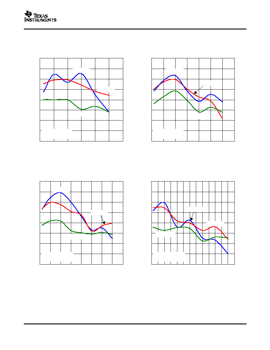
SPURIOUS-FREE DYNAMIC RANGE
SPURIOUS-FREE DYNAMIC RANGE
vs
vs
OUTPUT FREQUENCY
OUTPUT FREQUENCY
Figure 4.
Figure 5.
SPURIOUS-FREE DYNAMIC RANGE
SPURIOUS-FREE DYNAMIC RANGE
vs
vs
OUTPUT FREQUENCY
OUTPUT FREQUENCY
Figure 6.
Figure 7.
9
www.ti.com
f - Frequency - MHz
-100
-80
-60
-40
-20
0
0.0
7.8
15.6
23.4
31.2
39.0
f
data
= 78 MSPS
f
OUT
= 15 MHz
Dual Bus Mode
Power - dBm
G007
f - Frequency - MHz
-100
-80
-60
-40
-20
0
0.0
16.5
33.0
49.5
66.0
82.5
f
data
= 165 MSPS
f
OUT
= 30.1 MHz
Dual Bus Mode
Power - dBm
G008
f
O
- Output Frequency - MHz
60
65
70
75
80
85
90
95
0
5
10
15
20
25
30
35
T
wo-T
one IMD3 - dBc
f
data
= 78 MSPS
Dual Bus Mode
G009
f
O
- Output Frequency - MHz
50
55
60
65
70
75
80
85
90
95
100
0
10
20
30
40
50
T
wo-T
one IMD3 - dBc
f
data
= 165 MSPS
Dual Bus Mode
G010
DAC5662
SLAS425 ≠ JULY 2004
TYPICAL CHARACTERISTICS (continued)
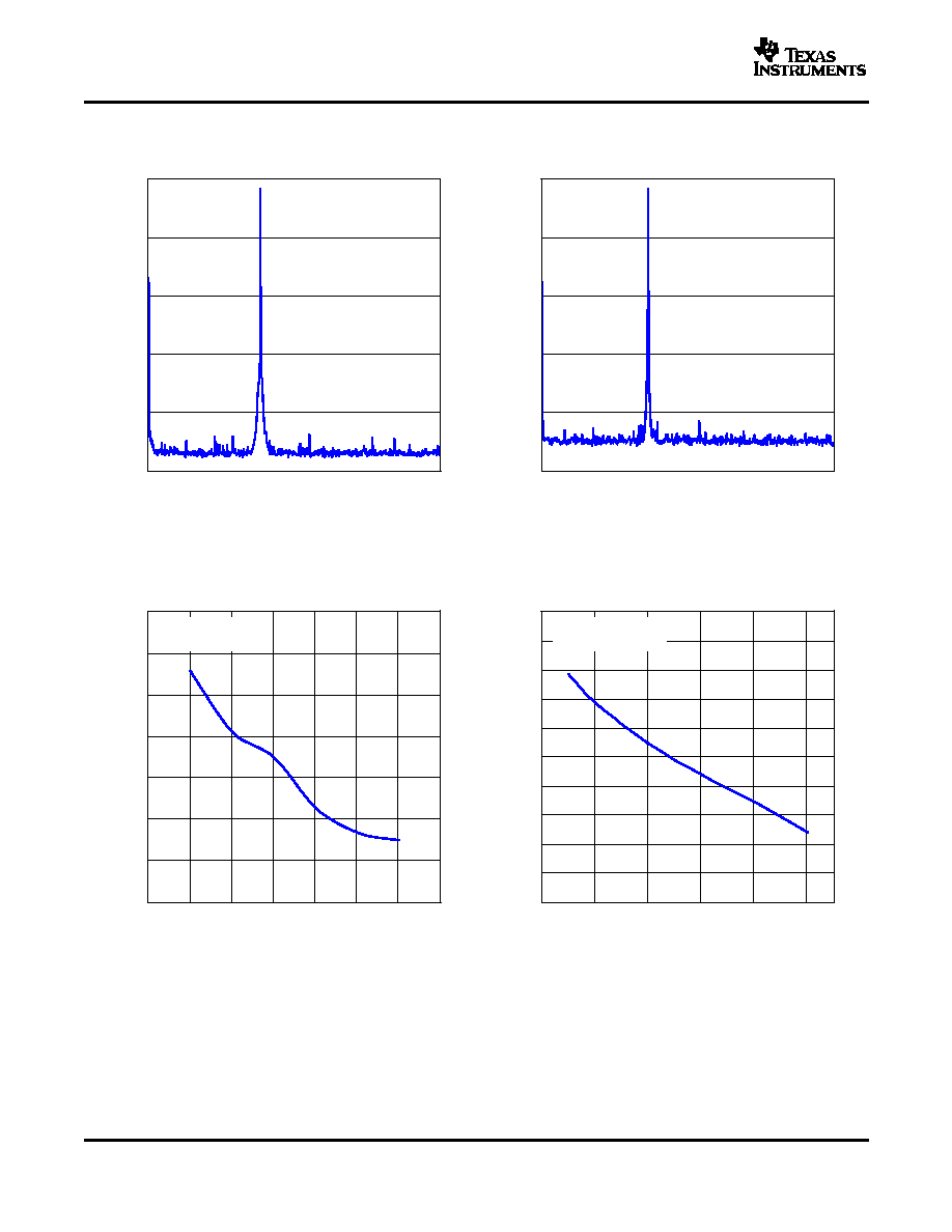
SINGLE-TONE SPECTRUM
SINGLE-TONE SPECTRUM
Figure 8.
Figure 9.
TWO-TONE IMD3
TWO-TONE IMD3
vs
vs
OUTPUT FREQUENCY
OUTPUT FREQUENCY
Figure 10.
Figure 11.
10
www.ti.com
f - Frequency - MHz
-100
-80
-60
-40
-20
0
19.0
19.5
20.0
20.5
21.0
21.5
22.0
Power - dBm
G011
f
data
= 78 MSPS
f
OUT
= 20.1 MHz
and 21.1 MHz
Dual Bus Mode
f - Frequency - MHz
-100
-80
-60
-40
-20
0
29.0
29.5
30.0
30.5
31.0
31.5
32.0
Power - dBm
G012
f
data
= 165 MSPS
f
OUT
= 30.1 MHz
and 31.1 Mhz
Dual Bus Mode
f - Frequency - MHz
-120
-100
-80
-60
-40
-20
0
1
2
3
4
5
6
7
8
9
10
f
data
= 122.88 MSPS
Baseband Signal
ACPR = 72 dB
Dual Bus Mode
Power - dBm
G013
f - Frequency - MHz
Power - dBm
G014
-120
-100
-80
-60
-40
-20
18 20 22 24 26 28 30 32 34 36 38 40 42 44
f
data
= 122.88 MSPS
IF = 30.72 MHz
ACPR = 72 dB
Dual Bus Mode
DAC5662
SLAS425 ≠ JULY 2004
TYPICAL CHARACTERISTICS (continued)
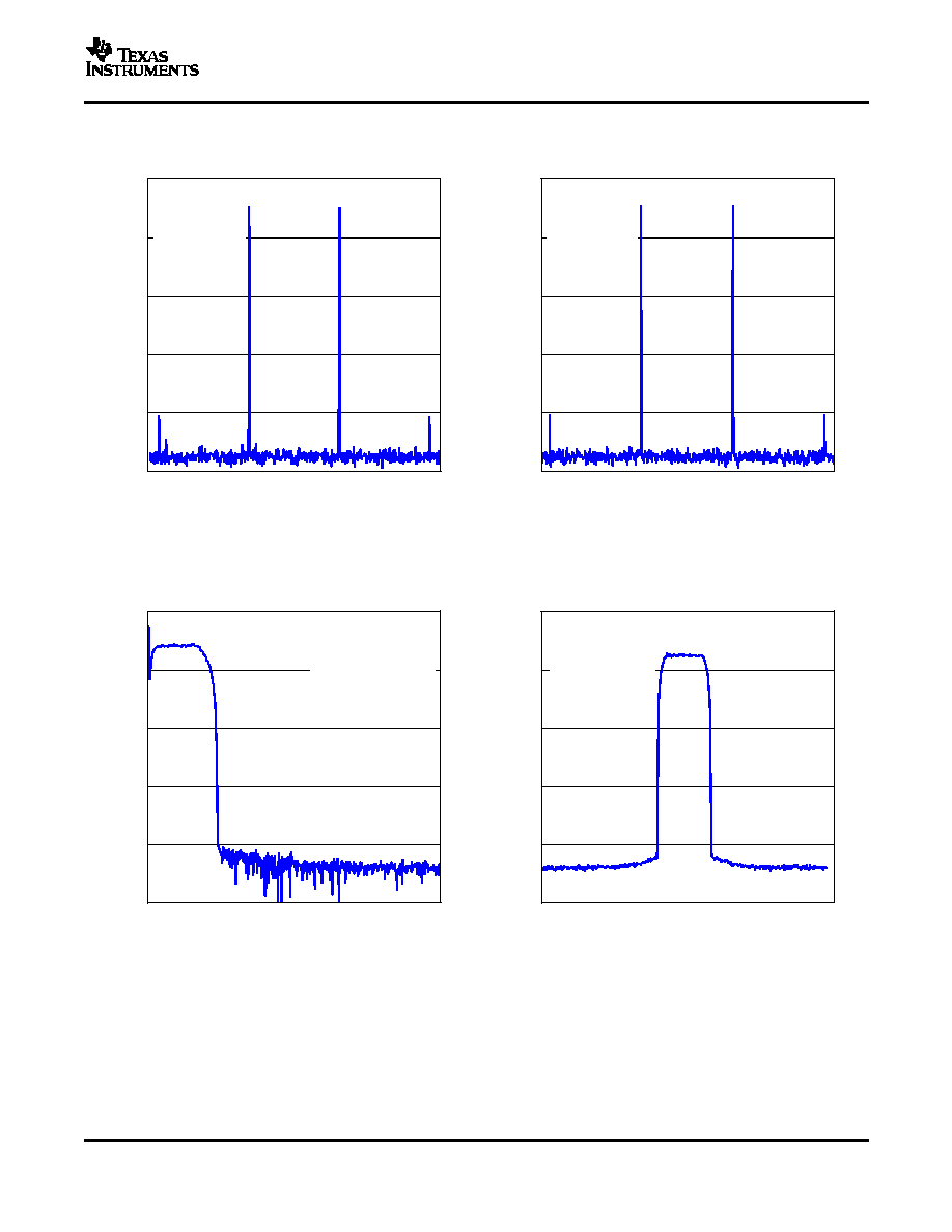
TWO-TONE SPECTRUM
TWO-TONE SPECTRUM
Figure 12.
Figure 13.
POWER
POWER
vs
vs
FREQUENCY
FREQUENCY
Figure 14.
Figure 15.
11
www.ti.com
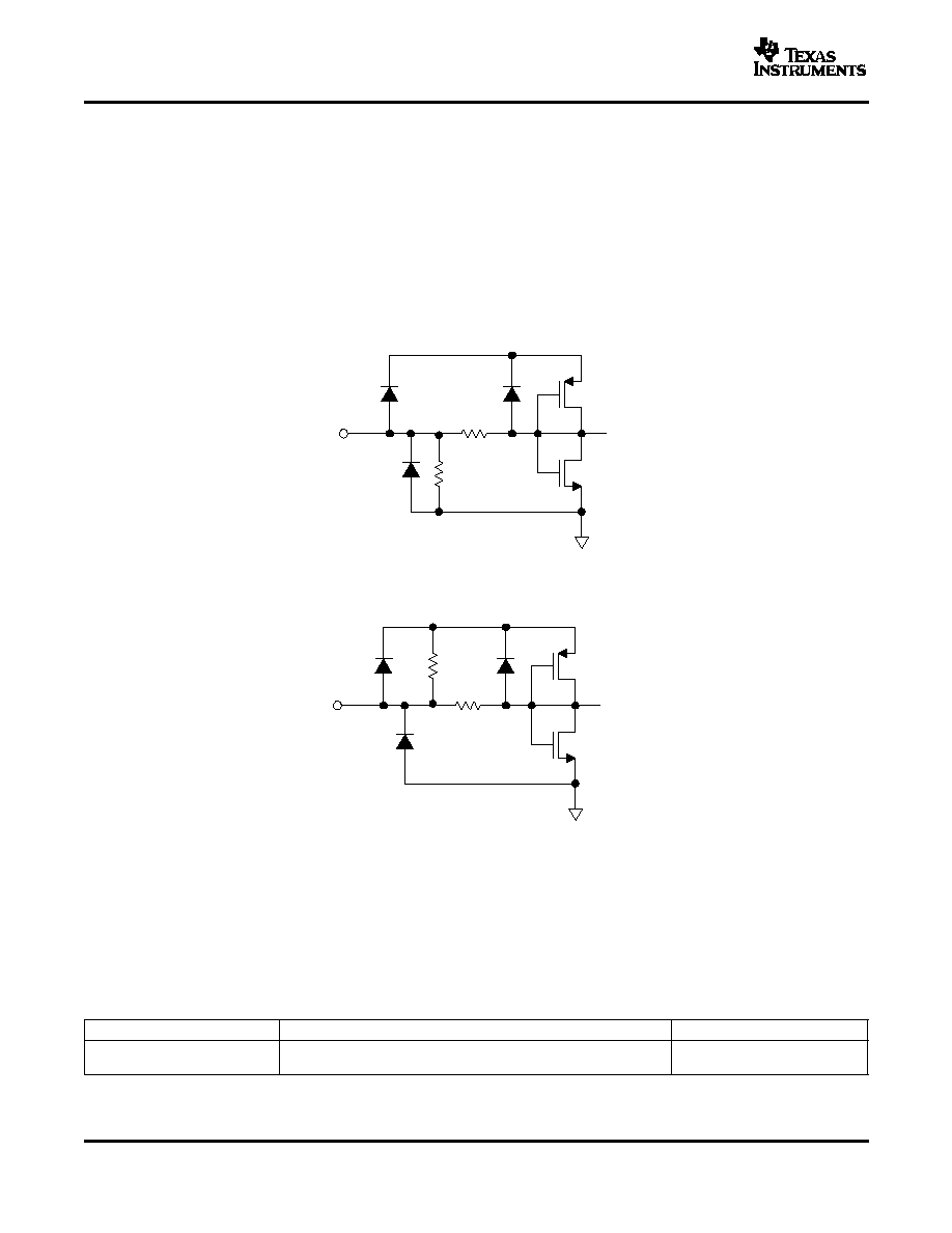
DIGITAL INPUTS AND TIMING
Digital Inputs
DA[11:0]
DB[11:0]
SLEEP
CLKA/B
WRTA/B
Internal
Digital In
DVDD
DGND
GSET
MODE
Internal
Digital In
DVDD
DGND
Input Interfaces
DAC5662
SLAS425 ≠ JULY 2004
The data input ports of the DAC5662 accept a standard positive coding with data bit D11 being the most
significant bit (MSB). The converter outputs support a clock rate of up to 200 MSPS. The best performance will
typically be achieved with a symmetric duty cycle for write and clock; however, the duty cycle may vary as long
as the timing specifications are met. Similarly, the setup and hold times may be chosen within their specified
limits.
All digital inputs of the DAC5662 are CMOS compatible. Figure 16 and Figure 17 show schematics of the
equivalent CMOS digital inputs of the DAC5662. The 12-bit digital data input follows the offset positive binary
coding scheme. The DAC5662 is designed to operate with a digital supply (DVDD) of 3 V to 3.6 V.
Figure 16. CMOS/TTL Digital Equivalent Input With Internal Pulldown Resistor
Figure 17. CMOS/TTL Digital Equivalent Input With Internal Pullup Resistor
The DAC5662 features two operating modes selected by the MODE pin, as shown in the following table
∑
For dual-bus input mode, the device essentially consists of two separate DACs. Each DAC has its own
separate data input bus, clock input, and data write signal (data latch-in).
∑
In single-bus interleaved mode, the data should be presented interleaved at the I-channel input bus. The
Q-channel input bus is not used in this mode. The clock and write input are now shared by both DACs.
MODE PIN
Mode pin connected to DGND
Mode pin connected to DVDD
Bus input
Single-bus interleaved mode, clock and write input equal for both
Dual-bus mode, DACs operate
DACs
independently
12

www.ti.com
Dual-Bus Data Interface and Timing
Valid Data
D[11:0]
t
su
t
h
t
lat
t
pd
t
settle
WRT1/
WRT2
CLK1/
CLK2
IOUT
or
IOUT
t
1ph
Single-Bus Interleaved Data Interface and Timing
DAC5662
SLAS425 ≠ JULY 2004
In dual-bus mode, the MODE pin is connected to DVDD. The two converter channels within the DAC5662 consist
of two independent, 12-bit, parallel data ports. Each DAC channel is controlled by its own set of write (WRTA,
WRTB) and clock (CLKA, CLKB) lines. The WRT lines control the channel input latches and the CLK lines
control the DAC latches. The data is first loaded into the input latch by a rising edge of the WRT line
The internal data transfer requires a correct sequence of write and clock inputs, since essentially two clock
domains having equal periods (but possibly different phases) are input to the DAC5662. This is defined by a
minimum requirement of the time between the rising edge of the clock and the rising edge of the write inputs.
This essentially implies that the rising edge of CLK must occur at the same time or before the rising edge of the
WRT signal. A minimum delay of 2 ns should be maintained if the rising edge of the clock occurs after the rising
edge of the write. Note that these conditions are satisfied when the clock and write inputs are connected
externally. Note that all specifications were measured with the WRT and CLK lines connected together.
Figure 18. Dual Bus Mode Operation
In single-bus interleaved mode, the MODE pin is connected to DGND. Figure 19 shows the timing diagram. In
interleaved mode, the I- and Q-channels share the write input (WRTIQ) and update clock (CLKIQ and internal
CLKDACIQ). Multiplexing logic directs the input word at the I-channel input bus to either the I-channel input latch
(SELECTIQ is high) or to the Q-channel input latch (SELECTIQ is low). When SELECTIQ is high, the data value
in the Q-channel latch is retained by presenting the latch output data to its input again. When SELECTIQ is low,
the data value in the I-channel latch is retained by presenting the latch output data to its input.
In interleaved mode, the I-channel input data rate is twice the update rate of the DAC core. As in dual-bus mode,
it is important to maintain a correct sequence of write and clock inputs. The edge-triggered flip-flops latch the I-
and Q-channel input words on the rising edge of the write input (WRTIQ). This data is presented to the I- and
Q-DAC latches on the following falling edge of the write inputs. The DAC5662 clock input is divided by a factor of
two before it is presented to the DAC latches.
Correct pairing of the I- and Q-channel data is done by RESETIQ. In interleaved mode, the clock input CLKIQ is
divided by two, which would translate to a non-deterministic relation between the rising edges of the CLKIQ and
CLKDACIQ. RESETIQ ensures, however, that the correct position of the rising edge of CLKDACIQ with respect
to the data at the input of the DAC latch is determined. CLKDACIQ is disabled (low) when RESETIQ is high.
13
www.ti.com
Valid Data
D[11:0]
t
su
t
h
t
lat
t
pd
t
settle
SELECTIQ
WRTIQ
CLKIQ
RESETIQ
IOUT
or
IOUT
DAC5662
SLAS425 ≠ JULY 2004
Figure 19. Single-Bus Interleaved Mode Operation
14

www.ti.com
APPLICATION INFORMATION
Theory of Operation
DAC Transfer Function
I
OUTFS
+
I
OUT1
)
I
OUT2
(1)
I
OUT1
+
I
OUTFS
Code
4096
(2)
I
OUT2
+
I
OUTFS
4095
*
Code
4096
(3)
I
OUTFS
+
32
I
REF
+
32
V
REF
R
SET
(4)
V
OUT1
+
I
OUT1
R
LOAD
(5)
V
OUT2
+
I
OUT2
R
LOAD
(6)
DAC5662
SLAS425 ≠ JULY 2004
The architecture of the DAC5662 uses a current steering technique to enable fast switching and high update
rate. The core element within the monolithic DAC is an array of segmented current sources that are designed to
deliver a full-scale output current of up to 20 mA. An internal decoder addresses the differential current switches
each time the DAC is updated and a corresponding output current is formed by steering all currents to either
output summing node, IOUT1 and IOUT2. The complementary outputs deliver a differential output signal, which
improves the dynamic performance through reduction of even-order harmonics, common-mode signals (noise),
and double the peak-to-peak output signal swing by a factor of two, compared to single-ended operation.
The segmented architecture results in a significant reduction of the glitch energy, improves the dynamic
performance (SFDR), and DNL. The current outputs maintain a very high output impedance of greater
than 300 k
.
When GSET is high (one resistor mode), the full-scale output current for both DACs is determined by the ratio of
the internal reference voltage (1.2 V) and an external resistor RSET connected to BIASJ_A. When GSET is low
(two resistor mode), the full-scale output current for each DACs is determined by the ratio of the internal
reference voltage (1.2 V) and separate external resistors RSET connected to BIASJ_A and BIASJ_B. The
resulting IREF is internally multiplied by a factor of 32 to produce an effective DAC output current that can range
from 2 mA to 20 mA, depending on the value of RSET.
The DAC5662 is split into a digital and an analog portion, each of which is powered through its own supply pin.
The digital section includes edge-triggered input latches and the decoder logic, while the analog section
comprises the current source array with its associated switches, and the reference circuitry.
Each of the DACs in the DAC5662 has a set of complementary current outputs, IOUT1 and IOUT2. The full-scale
output current, IOUTFS, is the summation of the two complementary output currents:
The individual output currents depend on the DAC code and can be expressed as:
where Code is the decimal representation of the DAC data input word. Additionally, IOUTFS is a function of the
reference current IREF, which is determined by the reference voltage and the external setting resistor (RSET).
In most cases, the complementary outputs drive resistive loads or a terminated transformer. A signal voltage
develops at each output according to:
The value of the load resistance is limited by the output compliance specification of the DAC5662. To maintain
specified linearity performance, the voltage for IOUT1 and IOUT2 should not exceed the maximum allowable
compliance range.
15
www.ti.com
V
OUTDIFF
+
V
OUT1
*
V
OUT2
(7)
V
OUTDIFF
+
(2
Code
*
4095)
4096
I
OUTFS
R
LOAD
(8)
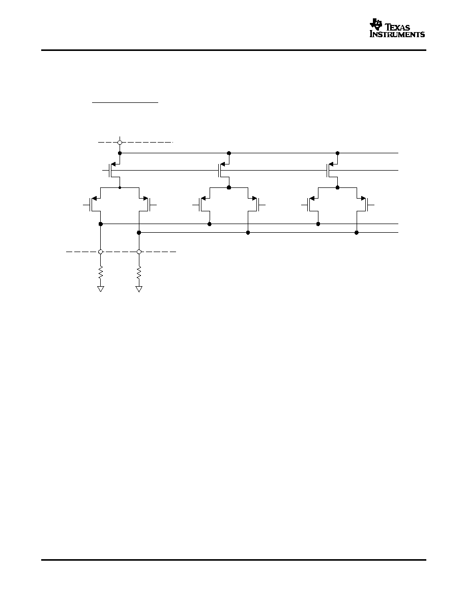
Analog Outputs
AVDD
Current Source Array
IOUT1
IOUT2
S(1)
S(1)C
R
LOAD
R
LOAD
S(2)
S(2)C
S(N)
S(N)C
Output Configurations
DAC5662
SLAS425 ≠ JULY 2004
APPLICATION INFORMATION (continued)
The total differential output voltage is:
Figure 20. Analog Outputs
The DAC5662 provides two complementary current outputs, IOUT1 and IOUT2. The simplified circuit of the
analog output stage representing the differential topology is shown in Figure 20. The output impedance of IOUT1
and IOUT2 results from the parallel combination of the differential switches, along with the current sources and
associated parasitic capacitances.
The signal voltage swing that may develop at the two outputs, IOUT1 and IOUT2, is limited by a negative and
positive compliance. The negative limit of ≠1 V is given by the breakdown voltage of the CMOS process and
exceeding it compromises the reliability of the DAC5662 or even causes permanent damage. With the full-scale
output set to 20 mA, the positive compliance equals 1.2 V. Note that the compliance range decreases to about 1
V for a selected output current of IOUTFS = 2 mA. Care should be taken that the configuration of DAC5662 does
not exceed the compliance range to avoid degradation of the distortion performance and integral linearity.
Best distortion performance is typically achieved with the maximum full-scale output signal limited to
approximately 0.5 Vpp. This is the case for a 50-
doubly terminated load and a 20-mA full-scale output current.
A variety of loads can be adapted to the output of the DAC5662 by selecting a suitable transformer while
maintaining optimum voltage levels at IOUT1 and IOUT2. Furthermore, using the differential output configuration
in combination with a transformer will be instrumental for achieving excellent distortion performance.
Common-mode errors, such as even-order harmonics or noise, can be substantially reduced. This is particularly
the case with high output frequencies.
For those applications requiring the optimum distortion and noise performance, it is recommended to select a
full-scale output of 20 mA. A lower full-scale range of 2 mA may be considered for applications that require low
power consumption, but can tolerate a slight reduction in performance level.
The current outputs of the DAC5662 allow for a variety of configurations. As mentioned previously, utilizing the
converter's differential outputs yield the best dynamic performance. Such a differential output circuit may consist
of an RF transformer or a differential amplifier configuration. The transformer configuration is ideal for most
applications with ac coupling, while op amps will be suitable for a dc-coupled configuration.
16

www.ti.com
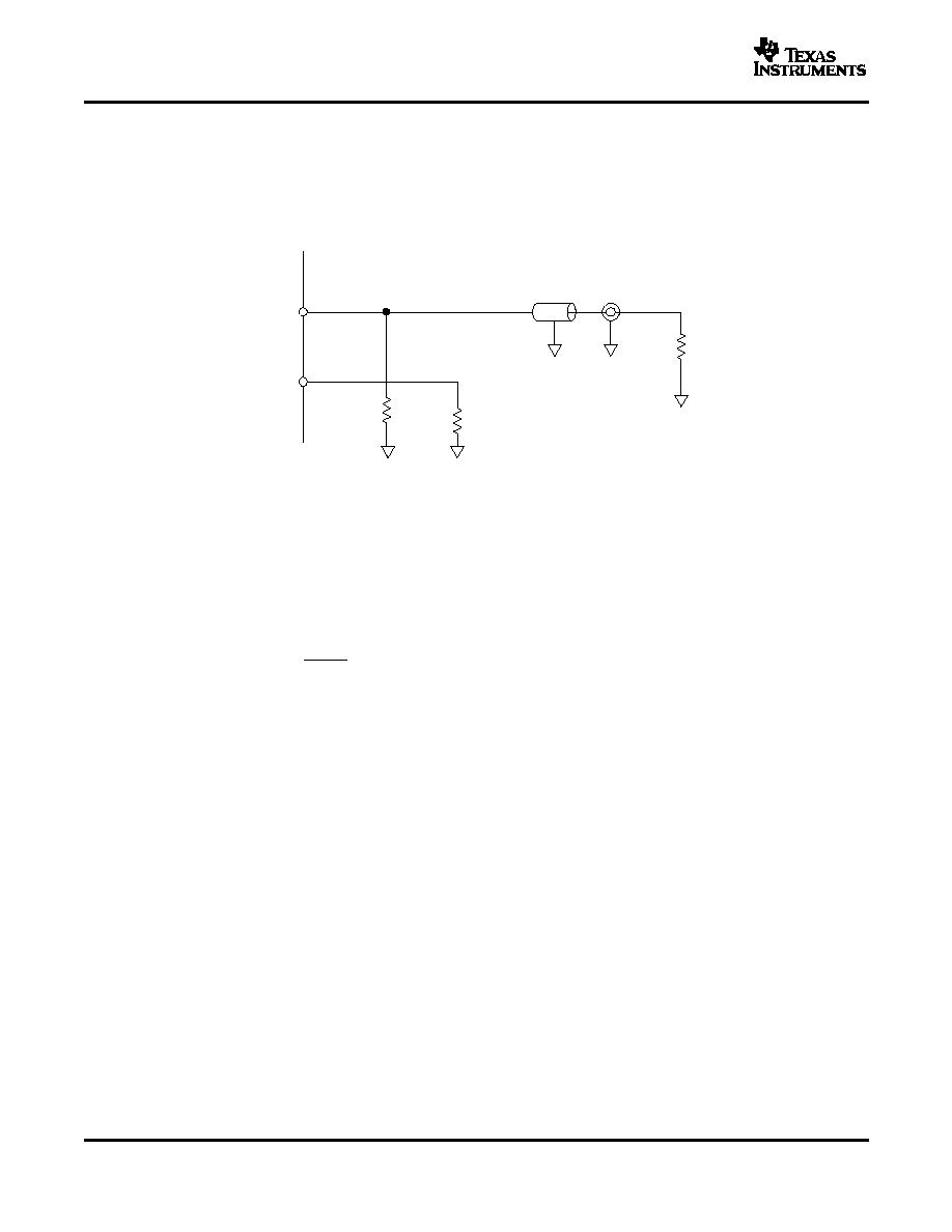
Differential With Transformer
IOUT1
1:1
IOUT2
50
50
R
LOAD
50
100
AGND
IOUT1
4:1
IOUT2
100
100
R
LOAD
50
AGND
DAC5662
SLAS425 ≠ JULY 2004
APPLICATION INFORMATION (continued)
The single-ended configuration may be considered for applications requiring a unipolar output voltage.
Connecting a resistor from either one of the outputs to ground converts the output current into a
ground-referenced voltage signal. To improve on the dc linearity by maintaining a virtual ground, an I-to-V or
op-amp configuration may be considered.
Using an RF transformer provides a convenient way of converting the differential output signal into a
single-ended signal while achieving excellent dynamic performance. The appropriate transformer should be
carefully selected based on the output frequency spectrum and impedance requirements.
The differential transformer configuration has the benefit of significantly reducing common-mode signals, thus
improving the dynamic performance over a wide range of frequencies. Furthermore, by selecting a suitable
impedance ratio (winding ratio) the transformer can be used to provide optimum impedance matching while
controlling the compliance voltage for the converter outputs.
Figure 21 and Figure 22 show 50-
doubly terminated transformer configurations with 1:1 and 4:1 impedance
ratios, respectively. Note that the center tap of the primary input of the transformer has to be grounded to enable
a dc-current flow. Applying a 20-mA full-scale output current would lead to a 0.5-Vpp output for a 1:1 transformer
and a 1-Vpp output for a 4:1 transformer. In general, the 1:1 transformer configuration will have slightly better
output distortion, but the 4:1 transformer will have 6 dB higher output power.
Figure 21. Driving a Doubly Terminated 50-
Cable Using a 1:1 Impedance Ratio Transformer
Figure 22. Driving a Doubly Terminated 50-
Cable Using a 4:1 Impedance Ratio Transformer
17
www.ti.com
Single-Ended Configuration
IOUT1
IOUT2
50
25
R
LOAD
50
AGND
Reference Operation
Internal Reference
I
OUTFS
+
32
I
REF
+
32
V
REF
R
SET
(9)
External Reference
DAC5662
SLAS425 ≠ JULY 2004
APPLICATION INFORMATION (continued)
Figure 23 shows the single-ended output configuration, where the output current I
OUT1
flows into an equivalent
load resistance of 25
. Node IOUT2 should be connected to AGND or terminated with a resistor of 25
to
AGND. The nominal resistor load of 25
gives a differential output swing of 1 Vpp when applying a 20-mA
full-scale output current.
Figure 23. Driving a Doubly Terminated 50-
Cable Using a Single-Ended Output
The DAC5662 has an on-chip reference circuit which comprises a 1.2-V bandgap reference and two control
amplifiers, one for each DAC. The full-scale output current, IOUTFS, of the DAC5662 is determined by the
reference voltage, VREF, and the value of resistor RSET. IOUTFS can be calculated by:
The reference control amplifier operates as a V-to-I converter producing a reference current, IREF, which is
determined by the ratio of VREF and RSET (see Equation 9). The full-scale output current, IOUTFS, results from
multiplying IREF by a fixed factor of 32.
Using the internal reference, a 2-k
resistor value results in a full-scale output of approximately 20 mA. Resistors
with a tolerance of 1% or better should be considered. Selecting higher values, the output current can be
adjusted from 20 mA down to 2 mA. Operating the DAC5662 at lower than 20-mA output currents may be
desirable for reasons of reducing the total power consumption, improving the distortion performance, or
observing the output compliance voltage limitations for a given load condition.
It is recommended to bypass the EXTIO pin with a ceramic chip capacitor of 0.1 µF or more. The control
amplifier is internally compensated and its small signal bandwidth is approximately 300 kHz.
The internal reference can be disabled by simply applying an external reference voltage into the EXTIO pin,
which in this case functions as an input. The use of an external reference may be considered for applications that
require higher accuracy and drift performance or to add the ability of dynamic gain control.
While a 0.1-µF capacitor is recommended to be used with the internal reference, it is optional for the external
reference operation. The reference input, EXTIO, has a high input impedance (1 M
) and can easily be driven
by various sources. Note that the voltage range of the external reference should stay within the compliance
range of the reference input.
18

www.ti.com
Gain Setting Option
Sleep Mode
DAC5662
SLAS425 ≠ JULY 2004
APPLICATION INFORMATION (continued)
The full-scale output current on the DAC5662 can be set two ways: either for each of the two DAC channels
independently or for both channels simultaneously. For the independent gain set mode, the GSET pin (pin 42)
must be low (i.e. connected to AGND). In this mode, two external resistors are required -- one RSET connected
to the BIASJ_A pin (pin 44) and the other to the BIASJ_B pin (pin 41). In this configuration, the user has the
flexibility to set and adjust the full-scale output current for each DAC independently, allowing for the
compensation of possible gain mismatches elsewhere within the transmit signal path.
Alternatively, bringing the GSET pin high (i.e. connected to AVDD), the DAC5662 switches into the simultaneous
gain set mode. Now the full-scale output current of both DAC channels is determined by only one external RSET
resistor connected to the BIASJ_A pin. The resistor at the BIASJ_2 pin may be removed, however this is not
required since this pin is not functional in this mode and the resistor has no effect on the gain equation.
The DAC5662 features a power-down function which can be used to reduce the total supply current to less than
3.5 mA over the specified supply range if no clock is present. Applying a logic high to the SLEEP pin initiates the
power-down mode, while a logic low enables normal operation. When left unconnected, an internal active
pulldown circuit enables the normal operation of the converter.
19
PACKAGING INFORMATION
Orderable Device
Status
(1)
Package
Type
Package
Drawing
Pins Package
Qty
Eco Plan
(2)
Lead/Ball Finish
MSL Peak Temp
(3)
DAC5662IPFB
ACTIVE
TQFP
PFB
48
250
Green (RoHS &
no Sb/Br)
CU NIPDAU
Level-2-260C-1 YEAR
DAC5662IPFBR
ACTIVE
TQFP
PFB
48
1000 Green (RoHS &
no Sb/Br)
CU NIPDAU
Level-2-260C-1 YEAR
DAC5662IPFBRG4
ACTIVE
TQFP
PFB
48
1000
None
Call TI
Call TI
(1)
The marketing status values are defined as follows:
ACTIVE: Product device recommended for new designs.
LIFEBUY: TI has announced that the device will be discontinued, and a lifetime-buy period is in effect.
NRND: Not recommended for new designs. Device is in production to support existing customers, but TI does not recommend using this part in
a new design.
PREVIEW: Device has been announced but is not in production. Samples may or may not be available.
OBSOLETE: TI has discontinued the production of the device.
(2)
Eco Plan - May not be currently available - please check
http://www.ti.com/productcontent
for the latest availability information and additional
product content details.
None: Not yet available Lead (Pb-Free).
Pb-Free (RoHS): TI's terms "Lead-Free" or "Pb-Free" mean semiconductor products that are compatible with the current RoHS requirements
for all 6 substances, including the requirement that lead not exceed 0.1% by weight in homogeneous materials. Where designed to be soldered
at high temperatures, TI Pb-Free products are suitable for use in specified lead-free processes.
Green (RoHS & no Sb/Br): TI defines "Green" to mean "Pb-Free" and in addition, uses package materials that do not contain halogens,
including bromine (Br) or antimony (Sb) above 0.1% of total product weight.
(3)
MSL, Peak Temp. -- The Moisture Sensitivity Level rating according to the JEDECindustry standard classifications, and peak solder
temperature.
Important Information and Disclaimer:The information provided on this page represents TI's knowledge and belief as of the date that it is
provided. TI bases its knowledge and belief on information provided by third parties, and makes no representation or warranty as to the
accuracy of such information. Efforts are underway to better integrate information from third parties. TI has taken and continues to take
reasonable steps to provide representative and accurate information but may not have conducted destructive testing or chemical analysis on
incoming materials and chemicals. TI and TI suppliers consider certain information to be proprietary, and thus CAS numbers and other limited
information may not be available for release.
In no event shall TI's liability arising out of such information exceed the total purchase price of the TI part(s) at issue in this document sold by TI
to Customer on an annual basis.
PACKAGE OPTION ADDENDUM
www.ti.com
11-Mar-2005
Addendum-Page 1
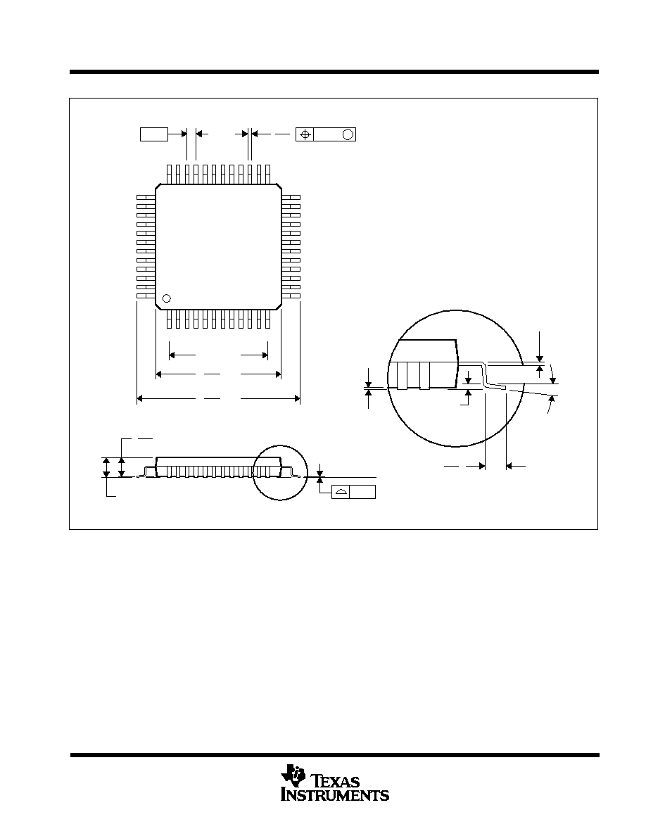
MECHANICAL DATA
MTQF019A ≠ JANUARY 1995 ≠ REVISED JANUARY 1998
POST OFFICE BOX 655303
∑
DALLAS, TEXAS 75265
PFB (S-PQFP-G48)
PLASTIC QUAD FLATPACK
4073176 / B 10/96
Gage Plane
0,13 NOM
0,25
0,45
0,75
Seating Plane
0,05 MIN
0,17
0,27
24
25
13
12
SQ
36
37
7,20
6,80
48
1
5,50 TYP
SQ
8,80
9,20
1,05
0,95
1,20 MAX
0,08
0,50
M
0,08
0
∞
≠ 7
∞
NOTES: A. All linear dimensions are in millimeters.
B. This drawing is subject to change without notice.
C. Falls within JEDEC MS-026

IMPORTANT NOTICE
Texas Instruments Incorporated and its subsidiaries (TI) reserve the right to make corrections, modifications,
enhancements, improvements, and other changes to its products and services at any time and to discontinue
any product or service without notice. Customers should obtain the latest relevant information before placing
orders and should verify that such information is current and complete. All products are sold subject to TI's terms
and conditions of sale supplied at the time of order acknowledgment.
TI warrants performance of its hardware products to the specifications applicable at the time of sale in
accordance with TI's standard warranty. Testing and other quality control techniques are used to the extent TI
deems necessary to support this warranty. Except where mandated by government requirements, testing of all
parameters of each product is not necessarily performed.
TI assumes no liability for applications assistance or customer product design. Customers are responsible for
their products and applications using TI components. To minimize the risks associated with customer products
and applications, customers should provide adequate design and operating safeguards.
TI does not warrant or represent that any license, either express or implied, is granted under any TI patent right,
copyright, mask work right, or other TI intellectual property right relating to any combination, machine, or process
in which TI products or services are used. Information published by TI regarding third-party products or services
does not constitute a license from TI to use such products or services or a warranty or endorsement thereof.
Use of such information may require a license from a third party under the patents or other intellectual property
of the third party, or a license from TI under the patents or other intellectual property of TI.
Reproduction of information in TI data books or data sheets is permissible only if reproduction is without
alteration and is accompanied by all associated warranties, conditions, limitations, and notices. Reproduction
of this information with alteration is an unfair and deceptive business practice. TI is not responsible or liable for
such altered documentation.
Resale of TI products or services with statements different from or beyond the parameters stated by TI for that
product or service voids all express and any implied warranties for the associated TI product or service and
is an unfair and deceptive business practice. TI is not responsible or liable for any such statements.
Following are URLs where you can obtain information on other Texas Instruments products and application
solutions:
Products
Applications
Amplifiers
amplifier.ti.com
Audio
www.ti.com/audio
Data Converters
dataconverter.ti.com
Automotive
www.ti.com/automotive
DSP
dsp.ti.com
Broadband
www.ti.com/broadband
Interface
interface.ti.com
Digital Control
www.ti.com/digitalcontrol
Logic
logic.ti.com
Military
www.ti.com/military
Power Mgmt
power.ti.com
Optical Networking
www.ti.com/opticalnetwork
Microcontrollers
microcontroller.ti.com
Security
www.ti.com/security
Telephony
www.ti.com/telephony
Video & Imaging
www.ti.com/video
Wireless
www.ti.com/wireless
Mailing Address:
Texas Instruments
Post Office Box 655303 Dallas, Texas 75265
Copyright
2005, Texas Instruments Incorporated