Document Outline
- FEATURES
- APPLICATIONS
- DESCRIPTION
- DEVICE INFORMATION
- functional block diagram
- Terminal Functions
- detailed description
- digital inputs
- clock input and timing
- supply inputs
- DAC transfer function
- reference operation
- analog current outputs
- sleep mode
- absolute maximum ratings over operating free-air temperature (unless ot\
herwise noted)
- recommended operating conditions
- ELECTRICAL SPECIFICATIONS
- electrical characteristics over recommended operating free-air temperatu\
re range, AV DD = 3.3 V,
DV DD = 3.3 V, I O(FS) = 20
- ˛ˇ
- electrical characteristics over recommended operating free-air temperatu\
re range, AV DD = 3.3 V,
DV DD = 3.3 V (unless other
- electrical characteristics over recommended operating free-air temperatu\
re range, AV DD = 3.3 V,
DV DD = 3.3 V, I O(FS) = 20
- LVDS input minimum and maximum input threshold and logical bit equivalen\
t
- TYPICAL CHARACTERISTICS
- DEFINITIONS
- definitions of specifications and terminology
- DAC5675 evaluation board
- MECHANICAL DATA
- PHP (S-PQFP-G48) PowerPAD PLASTIC QUAD FLATPACK
- IMPORTANT NOTICE

DAC5675
SLAS352B ≠ DECEMBER 2001 ≠ REVISED JUNE 2002
14-BIT, 400-MSPS
DIGITAL-TO-ANALOG CONVERTER
1
www.ti.com
FEATURES
D
400-MSPS Update Rate
D
LVDS-Compatible Input Interface
D
Spurious Free Dynamic Range (SFDR) to
Nyquist
≠ 69 dBc at 70-MHz IF, 400 MSPS
D
W-CDMA Adjacent Channel Power Ratio
ACPR
≠ 73 dBc at 30.72-MHz IF, 122.88 MSPS
≠ 71 dBc at 61.44-MHz IF, 245.76 MSPS
D
Differential Scalable Current Outputs: 2 mA to
20 mA
D
On-Chip 1.2-V Reference
D
Single 3.3-V Supply Operation
D
Power Dissipation: 820 at f
clk
= 400 MSPS,
f
out
= 70 MHz
D
Package: 48-Pin HTQFP PowerPad
,
T
JA
= 28.8
∞
C/W
APPLICATIONS
D
Cellular Base Transceiver Station Transmit
Channel
≠ CDMA: WCDMA, CDMA2000, IS≠95
≠ TDMA: GSM, IS≠136, EDGE/GPRS
≠ Supports Single-Carrier and Multicarrier
Applications
D
Test and Measurement: Arbitrary Waveform
Generation
D
Direct Digital Synthesis (DDS)
D
Cable Modem Headend
DESCRIPTION
The DAC5675 is a 14-bit resolution high
-
speed
digital-to-analog converter. The DAC5675 is designed
for high-speed digital data transmission in wired and
wireless communication systems, high-frequency
direct-digital synthesis (DDS), and waveform
reconstruction in test and measurement applications.
The DAC5675 has excellent spurious free dynamic
range (SFDR) at high intermediate frequencies, which
makes the DAC5675 well suited for multicarrier
transmission in TDMA and CDMA based cellular base
transceiver stations BTS.
The DAC5675 operates from a single-supply voltage of
3.3 V. Power dissipation is 820 mW at f
clk
= 400 MSPS,
f
out
= 70 MHz. The DAC5675 provides a nominal
full-scale differential current output of 20 mA,
supporting both single-ended and differential
applications. The output current can be directly fed to
the load with no additional external output buffer
required. The output is referred to the analog supply
voltage AVDD.
The DAC5675 is manufactured on Texas Instruments
advanced high-speed mixed-signal BiCMOS process.
The DAC5675 comprises a LVDS (low-voltage
differential signaling) interface. LVDS features a low
differential voltage swing with a low constant power
consumption across frequency, allowing for high speed
data transmission with low noise levels, i.e., low
electromagnetic interference (EMI). LVDS is typically
implemented in low-voltage digital CMOS processes,
making it the ideal technology for high-speed interfacing
between the DAC5675 and high-speed low-voltage
CMOS ASICs or FPGAs. The DAC5675 current-
source-array architecture supports update rates of up to
400 MSPS. On-chip edge-triggered input latches
provide for minimum setup and hold times thereby
relaxing interface timing.
PRODUCTION DATA information is current as of publication date.
Products conform to specifications per the terms of Texas Instruments
standard warranty. Production processing does not necessarily include
testing of all parameters.
PowerPAD is a trademark of Texas Instruments.
Copyright
2002, Texas Instruments Incorporated
Please be aware that an important notice concerning availability, standard warranty, and use in critical applications of
Texas Instruments semiconductor products and disclaimers thereto appears at the end of this data sheet.

DAC5675
SLAS352B ≠ DECEMBER 2001 ≠ REVISED JUNE 2002
2
www.ti.com
DESCRIPTION (continued)
The DAC5675 has been specifically designed for a differential transformer coupled output with a 50-
doubly
terminated load. With the 20-mA full-scale output current, both a 4:1 impedance ratio (resulting in an output
power of 4 dBm) and 1:1 impedance ratio transformer (-2 dBm) is supported. The last configuration is preferred
for optimum performance at high output frequencies and update rates. The output voltage compliance ranges
from 2.15 V to AVDD + 0.03 V.
An accurate on-chip 1.2-V temperature compensated bandgap reference and control amplifier allows the user
to adjust this output current from 20 mA down to 2 mA. This provides 20-dB gain range control capabilities.
Alternatively, an external reference voltage may be applied. The DAC5675 features a SLEEP mode, which
reduces the standby power to approximately 150 mW.
The DAC5675 is available in a 48-pin HTQPP thermally enhanced PowerPad package. This package increases
thermal efficiency in a standard size IC package. The device is characterized for operation over the industrial
temperature range of ≠40
∞
C to 85
∞
C.
14 15
D0B
D0A
D1B
D1A
D2B
D2A
D3B
D3A
D4B
D4A
D5B
D5A
36
35
34
33
32
31
30
29
28
27
26
25
16
1
2
3
4
5
6
7
8
9
10
11
12
D13A
D13B
D12A
D12B
D11A
D11B
D10A
D10B
D9A
D9B
D8A
D8B
17 18 19 20
47 46 45 44 43
48
42
40 39 38
41
21 22 23 24
37
13
PHP PACKAGE
(TOP VIEW)
A
VDD
AGND
AGND
A
VDD
IOUT2
IOUT1
A
VDD
AGND
EXTIO
BIASJ
DLLOFF
SLEEP
D7A
D7B
DVDD
DGND
DVDD
DGND
AGND
A
VDD
CLKC
CLK
D6A
D6B
AVAILABLE OPTIONS
T
PACKAGED DEVICE
TA
48-HTQFP PowerPAD PLASTIC QUAD FLATPACK
40
∞
C to 85
∞
C
DAC5675IPHP
≠ 40
∞
C to 85
∞
C
DAC5675IPHPR

DAC5675
SLAS352B ≠ DECEMBER 2001 ≠ REVISED JUNE 2002
3
www.ti.com
functional block diagram
EXTIO
Current
Source
Array
BIASJ
≠
+
Control Amp
SLEEP
Output
Current
Switches
DAC
Latch
+
Drivers
LVDS
Input
Interface
Input
Latches
D[13:0]B
14
14
Decoder
Bandgap
Reference
1.2 V
CLK
CLKC
+
≠
IBIAS
IOUT1
IOUT2
AVDD(4x)
AGND(4x)
DLL
DLLOFF
DAC5675
D[13:0]A
DVDD(2x)
DGND(2x)

DAC5675
SLAS352B ≠ DECEMBER 2001 ≠ REVISED JUNE 2002
4
www.ti.com
Terminal Functions
TERMINAL
I/O
DESCRIPTION
NAME
NO.
I/O
DESCRIPTION
AGND
19, 41, 46, 47
I
Analog negative supply voltage (ground)
AVDD
20, 42, 45, 48
I
Analog positive supply voltage
BIASJ
39
O
Full-scale output current bias
CLK
22
I
External clock input
CLKC
21
I
Complementary external clock input
D[13..0]A
1, 3, 5, 7, 9, 11,
13, 23, 25, 27,
29, 31, 33, 35
I
LVDS positive input, data bits 0 through 13
D13A is most significant data bit (MSB)
D0A is least significant data bit (MSB)
D[13..0]B
2, 4, 6, 8, 10, 12,
14, 24, 26, 28,
30, 32, 34, 36
I
LVDS negative input, data bits 0 through 13
D13B is most significant data bit (MSB)
D0B is least significant data bit (MSB)
DGND
16, 18
I
Digital negative supply voltage (ground)
DLLOFF
38
I
High DLL off / Low = DLL on
DVDD
15, 17
I
Digital positive supply voltage
EXTIO
40
I/O
Internal reference output or external reference input. Requires a 0.1-
µ
F decoupling capacitor to AGND
when used as reference output.
IOUT1
43
O
DAC current output. Full scale when all input bits are set 1. Connect reference side of DAC load
resistors to AVDD
IOUT2
44
O
DAC complementary current output. Full scale when all input bits are 0. Connect reference side of DAC
load resistors to AVDD
SLEEP
37
I
Asynchronous hardware power down input. Active high. Internally pulldown

DAC5675
SLAS352B ≠ DECEMBER 2001 ≠ REVISED JUNE 2002
5
www.ti.com
detailed description
Figure 1 shows a simplified block diagram of the current steering DAC5675. The DAC5675 consists of a
segmented array of non-transistor current sources, capable of delivering a full-scale output current up to 20 mA.
Differential current switches direct the current of each current source to either one of the complementary output
nodes IOUT1 or IOUT2. The complementary current output thus enables differential operation, canceling out
common mode noise sources (digital feed-through, on-chip and PCB noise), dc offsets, even order distortion
components, thereby doubling signal output power.
The full-scale output current is set using an external resistor (R
BIAS
) in combination with an on-chip bandgap
voltage reference source (1.2 V) and control amplifier. The current (I
BIAS
) through resistor R
BIAS
is mirrored
internally to provide a full-scale output current equal to 16 times I
BIAS
. The full-scale current is adjustable from
20 mA down to 2 mA by using the appropriate bias resistor value.
EXTIO
Current
Source
Array
BIASJ
≠
+
Control Amp
SLEEP
Output
Current
Switches
DAC
Latch
+
Drivers
LVDS
Input
Interface
Input
Latches
D[13:0]B
14
14
Decoder
Bandgap
Reference
1.2 V
CLK
CLKC
+
≠
IBIAS
IOUT1
IOUT2
AVDD(4x)
AGND(4x)
DLL
DLLOFF
DAC5675
D[13:0]A
DVDD(2x)
DGND(2x)
50
100
3.3 V
(AVDD)
50
3.3 V
(AVDD)
RLOAD
50
Output
1:1
3.3 V
(AVDD)
RT
200
1:4
Clock
Input
RBIAS
1 k
1 k
0.1
µ
F
CEXT
0.1
µ
F
3.3 V
3.3 V
Figure 1. Application Schematic

DAC5675
SLAS352B ≠ DECEMBER 2001 ≠ REVISED JUNE 2002
6
www.ti.com
detailed description (continued)
digital inputs
The DAC5675 comprises a low voltage differential signaling (LVDS) bus input interface. The LVDS features a
low differential voltage swing with low constant power consumption (~4 mA per complementary data input)
across frequency. The differential characteristic of LVDS allows for high-speed data transmission with low
electromagnetic interference (EMI) levels. The LVDS input minimum and maximum input threshold table lists
the LVDS input levels. Figure 2 shows the equivalent complementary digital input interface for the DAC5675,
valid for pins D[13..0]A and D[13..0]B. Note that the LVDS interface features internal 110-
resistors for proper
termination. Figure 3 shows the LVDS input timing measurement circuit and waveforms. A common mode level
of 1.2 V and a differential input swing of 0.8 V is applied to the inputs.
Internal
Digital In
D[13:0]A
D[13:0]B
AGND
AVDD
Internal
Digital In
D[13:0]A
D[13:0]B
DAC5675
DAC5675
100-
Termination
Resistor
Figure 2. LVDS Digital Equivalent Input
VB
VA
VA,B
1.4 V
1 V
0.4 V
≠0.4 V
0 V
Logical Bit
Equivalent
0
1
AGND
AVDD
DAC5675
V
COM
+
V
A
)
V
B
2
VB
VA
VA,B
Figure 3. LVDS Timing Test Circuit and Input Test Levels

DAC5675
SLAS352B ≠ DECEMBER 2001 ≠ REVISED JUNE 2002
7
www.ti.com
digital inputs (continued)
Figure 4 shows a schematic of the equivalent CMOS/TTL-compatible digital inputs of the DAC5675, valid for
pins SLEEP and DLLOFF.
Digital Input
Internal
Digital In
DVDD
DGND
DAC5675
Figure 4. CMOS/TTL Digital Equivalent Input
clock input and timing
The DAC5675 comprises a delay locked loop DLL for internal clock alignment. Enabling the DLL is controlled
by pin DLLOFF. The DLL should be enabled for update rates in excess of 100 MSPS. The DLL works only to
maximize setup and hold times of the digital input and does not affect the analog output of the DAC. Figure 5
shows the clock and data input timing diagram. The DAC5675 features a differential clock input. Internal
edge-triggered flip-flops latch the input word on the rising edge of the positive clock input CLK (falling edge of
the negative/complementary clock input CLKC). The DAC core is updated with the data word on the following
rising edge of the positive clock input CLK (falling edge of CLKC). This results in a conversion latency of one
clock cycle. The DAC5675 provides for minimum setup and hold times (>0.25 ns), allowing for noncritical
external interface timing. The clock duty cycle can be chosen arbitrarily under the timing constraints listed in
the electrical characteristics section. However, a 50% duty cycle gives the optimum dynamic performance.
The DAC5675 clock input can be driven by a differential sine wave. The ac coupling, in combination with internal
biasing ensures that the sine wave input is centered at the optimum common-mode voltage that is required for
the internal clock buffer. The DAC5675 clock input can also be driven single-ended, this is shown in Figure 6.
The best SFDR performance is typically achieved by driving the inputs differentially.

DAC5675
SLAS352B ≠ DECEMBER 2001 ≠ REVISED JUNE 2002
8
www.ti.com
clock input and timing (continued)
CLK
D[13:0]A
DAC Output
IOUT1/IOUT2
0.1%
0.1%
50%
Valid Data
50%
50%
50%
50%
50%
90%
10%
CLKC
D[13:0]B
tsu(D)
th(D)
td(D) = 1/fCLK
tw(L)
ts(DAC)
tpd
tr(IOUT)
tw(H)
Figure 5. Timing Diagram
AVDD
CLK
Internal
Digital In
CLKC
AGND
R1
1 k
DAC5675
R1
1 k
R2
2 k
R2
2 k
RT
200
CLK
1:4
CLKC
Termination Resistor
Swing Limitation
DAC5675
Optional, May Be Bypassed
CAC
0.1
µ
F
Figure 6. Clock Equivalent Input

DAC5675
SLAS352B ≠ DECEMBER 2001 ≠ REVISED JUNE 2002
9
www.ti.com
clock input and timing (continued)
Figure 7 shows the equivalent schematic of the differential clock input buffer. The input nodes are internally
self-biased enabling ac coupling of the clock inputs. Figure 8 shows the preferred configuration for driving the
DAC5675.
Ropt
22
Node CLKC
Internally Biased
DAC5675
TTL/CMOS Source
0.01
µ
F
CLK
CLKC
Figure 7. Driving the DAC5675 With a Single-Ended TTL/CMOS Clock Source
RT
50
DAC5675
CAC
0.01
µ
F
CAC
0.01
µ
F
RT
50
VTT
Differential
ECL
or
(LV)PECL
Source
+
≠
CLK
CLKC
Figure 8. Driving the DAC5675 With a Differential ECL/PECL Clock Source
RT
50
DAC5675
CAC
0.01
µ
F
CAC
0.01
µ
F
RT
50
VTT
Single-Ended
ECL
or
(LV)PECL
Source
ECL/PECL
Gate
CLK
CLKC
Figure 9. Driving the DAC5675 With a Single-Ended ECL/PECL Clock Source

DAC5675
SLAS352B ≠ DECEMBER 2001 ≠ REVISED JUNE 2002
10
www.ti.com
detailed description (continued)
supply inputs
The DAC5675 comprises separate analog and digital supplies, i.e., AV
DD
and DV
DD
respectively. These supply
inputs can be set independently from 3.6 V down to 3.15 V.
DAC transfer function
The DAC5675 delivers complementary output currents IOUT1 and IOUT2. The DAC supports straight binary
coding, with D13 being the MSB and D0 the LSB (For ease of notation we denote D13..D10 as the logical bit
equivalent of the complementary LVDS inputs D[13..0]A and D[13..0]B). Output current IOUT1 equals the
approximate full-scale output current when all input bits are set high, i.e., the binary input word has the decimal
representation 16383. Full-scale output current flows through terminal IOUT2 when all input bits are set low
(mode 0, straight binary input). The relation between IOUT1 and IOUT2 can thus be expressed as:
IOUT1 = IO
(FS)
≠ IOUT2
where IO
(FS)
is the full-scale output current. The output currents can be expressed as:
IOUT1
+
I
O(FS)
CODE
16384
IOUT2
+
I
O(FS)
(16383≠CODE)
16384
where CODE is the decimal representation of the DAC data input word. Output currents IOUT1 and IOUT2 drive
resistor loads R
L
or a transformer with equivalent input load resistance R
L
. This would translate into
single-ended voltages VOUT1 and VOUT2 at terminal IOUT1 and IOUT2, respectively, of:
VOUT1
+
IOUT1
R
L
+
CODE
16384
I
O(FS)
R
L
VOUT2
+
IOUT2
R
L
+
(16383≠CODE)
16384
I
O(FS)
R
L
The differential output voltage VOUT
(DIFF)
can thus be expressed as:
VOUT
(DIFF)
+
VOUT1
*
VOUT2
+
(2CODE
*
16383)
16384
I
O(FS)
R
L
The latter equation shows that applying the differential output results in doubling of the signal power delivered
to the load. Since the output currents IOUT1 and IOUT2 are complementary, they become additive when
processed differentially. Note that care should be taken not to exceed the compliance voltages at node IOUT1
and IOUT2, which leads to increased signal distortion.

DAC5675
SLAS352B ≠ DECEMBER 2001 ≠ REVISED JUNE 2002
11
www.ti.com
detailed description (continued)
reference operation
The DAC5675 comprises a bandgap reference and control amplifier for biasing the full-scale output current. The
full-scale output current is set by applying an external resistor R
BIAS
. The bias current I
BIAS
through resistor
R
BIAS
is defined by the on-chip bandgap reference voltage and control amplifier. The full-scale output current
equals 16 times this bias current. The full-scale output current IO
(FS)
is thus expressed as:
I
O(FS)
+
16
I
BIAS
+
16
V
EXTIO
R
BIAS
where V
EXTIO
is the voltage at terminal EXTIO. The bandgap reference voltage delivers an accurate voltage
of 1.2 V. This reference can be override by applying a external voltage to terminal EXTIO. The bandgap
reference can additionally be used for external reference operation. In that case, an external buffer with high
impedance input should be applied in order to limit the bandgap load current to a maximum of 100 nA. The
capacitor C
EXT
may be omitted. Terminal EXTIO serves as either a input or output node. The full-scale output
current is adjustable from 20 mA down to 2 mA by varying resistor R
BIAS
.
analog current outputs
Figure 10 shows a simplified schematic of the current source array output with corresponding switches.
Differential non switches direct the current of each individual PMOS current source to either the positive output
node IOUT1 or its complementary negative output node IOUT2. The output impedance is determined by the
stack of the current sources and differential switches, and is >300 k
in parallel with an output capacitance of
5 pF.
The external output resistors are referred to the positive supply AVDD.
Current Source Array
IOUT2
3.3 V
(AVDD)
RLOAD
S(1)
S(1)C
S(2)
S(2)C
S(N)
S(N)C
AGND
DAC5675
IOUT1
RLOAD
Figure 10. Equivalent Analog Current Output

DAC5675
SLAS352B ≠ DECEMBER 2001 ≠ REVISED JUNE 2002
12
www.ti.com
analog current outputs (continued)
The DAC5675 can easily be configured to drive a doubly terminated 50-
cable using a properly selected
transformer. Figure 11 and Figure 12 show the 1:1 and 4:1 impedance ratio configuration. These configurations
provide maximum rejection of common-mode noise sources and even order distortion components, thereby
doubling the DAC's power to the output. The center tap on the primary side of the transformer is terminated to
AVDD, enabling a dc current flow for both IOUT1 and IOUT2. Note that the ac performance of the DAC5675
is optimum and specified using a 1:1 differential transformer coupled output.
IOUT1
1:1
IOUT2
DAC5675
3.3 V
(AVDD)
50
50
3.3 V
(AVDD)
3.3 V
(AVDD)
RLOAD
50
100
Figure 11. Driving a Doubly Terminated 50-
Cable Using a 1:1 Impedance Ratio Transformer
4:1
DAC5675
3.3 V
(AVDD)
100
100
3.3 V
(AVDD)
3.3 V
(AVDD)
RLOAD
50
IOUT1
IOUT2
15
Figure 12. Driving a Doubly Terminated 50-
Cable Using a 4:1 Impedance Ratio Transformer

DAC5675
SLAS352B ≠ DECEMBER 2001 ≠ REVISED JUNE 2002
13
www.ti.com
analog current outputs (continued)
Figure 13(a) shows the typical differential output configuration with two external matched resistor loads. The
nominal resistor load of 25
gives a differential output swing of 1 V
PP
(0.5-V
PP
single-ended) when applying
a 20-mA full-scale output current. The output impedance of the DAC5675 slightly depends on the output voltage
at nodes IOUT1 and IOUT2. Consequently, for optimum dc-integral nonlinearity, the configuration of
Figure 13(b) should be chosen. In this current/voltage (I-V) configuration, terminal IOUT1 is kept at AVDD by
the inverting operational amplifier. The complementary output should be connected to AVDD to provide a
dc-current path for the current sources switched to IOUT1. The amplifier's maximum output swing and the DACs
full-scale output current determine the value of the feedback resistor (R
FB
). The capacitor (C
FB
) filters the steep
edges of the DAC5675 current output, thereby reducing the operational amplifier's slew-rate requirements. In
this configuration, the op amp should operate at a supply voltage higher than the resistors output reference
voltage AVDD due to its positive and negative output swing around AVDD. Node IOUT1 should be selected if
a single-ended unipolar output is desired.
DAC5675
3.3 V
(AVDD)
25
25
3.3 V
(AVDD)
VOUT1
VOUT2
Optional, For
Single-Ended
Output Referred
to AVDD
DAC5675
3.3 V
(AVDD)
+
≠
VOUT
200
Cfb
IOUT1
IOUT2
IOUT1
IOUT2
(a) Unbuffered Differential and
Single-Ended Resistor and Buffered
(b) Buffered Single-Ended Output Configuration
Figure 13. Output Configurations
sleep mode
The DAC5675 features a power-down mode that turns off the output current and reduces the supply current
to approximately 45 mA. The power-down mode is activated by applying a logic level 1 to the SLEEP pin (e.g.,
by connecting the SLEEP pin to the AVDD pin). The SLEEP pin must be connected. Power-up and power-down
activation times depend on the value of the external capacitor at node SLEEP. For a nominal capacitor value
of 0.1-
µ
F, powerdown takes less than 5
µ
s and approximately 3 ms to power back up.

DAC5675
SLAS352B ≠ DECEMBER 2001 ≠ REVISED JUNE 2002
14
www.ti.com
absolute maximum ratings over operating free-air temperature (unless otherwise noted)
Supply voltage range:
AV
DD
≠0.3 V to 3.6 V
. . . . . . . . . . . . . . . . . . . . . . . . . . . . . . . . . . . . . . . . . . . . . . . . . . . . . . . . . .
DV
DD
ß
≠0.3 V to 3.6 V
. . . . . . . . . . . . . . . . . . . . . . . . . . . . . . . . . . . . . . . . . . . . . . . . . . . . . . . . . .
AV
DD
to DV
DD
≠3.6 V to 3.6 V
. . . . . . . . . . . . . . . . . . . . . . . . . . . . . . . . . . . . . . . . . . . . . . . . . . .
Voltage between AGND and DGND
≠0.3 V to 0.5 V
. . . . . . . . . . . . . . . . . . . . . . . . . . . . . . . . . . . . . . . . . . . . . . . . . . . . . . .
CLK, CLKC, SLEEP
ß
≠0.3 V to DVDD + 0.3 V
. . . . . . . . . . . . . . . . . . . . . . . . . . . . . . . . . . . . . . . . . . . . . . . . . . . . . . . . . . .
Digital input D[13..0]A, D[13..0]B
ß
≠0.3 V to DVDD + 0.3 V
. . . . . . . . . . . . . . . . . . . . . . . . . . . . . . . . . . . . . . . . . . . . . . . .
IOUT1, IOUT2
≠1.0 V to AVDD + 0.3 V
. . . . . . . . . . . . . . . . . . . . . . . . . . . . . . . . . . . . . . . . . . . . . . . . . . . . . . . . . . . . . . . .
EXTIO, BIASJ
≠0.3 V to AVDD + 0.3 V
. . . . . . . . . . . . . . . . . . . . . . . . . . . . . . . . . . . . . . . . . . . . . . . . . . . . . . . . . . . . . . . .
Peak input current (any input)
20 mA
. . . . . . . . . . . . . . . . . . . . . . . . . . . . . . . . . . . . . . . . . . . . . . . . . . . . . . . . . . . . . . . . . . .
Peak total input current (all inputs)
≠30 mA
. . . . . . . . . . . . . . . . . . . . . . . . . . . . . . . . . . . . . . . . . . . . . . . . . . . . . . . . . . . . . .
Operating free-air temperature range, T
A
(DAC5675I)
≠40
∞
C to 85
∞
C
. . . . . . . . . . . . . . . . . . . . . . . . . . . . . . . . . . . . . . .
Storage temperature range
≠65
∞
C to 150
∞
C
. . . . . . . . . . . . . . . . . . . . . . . . . . . . . . . . . . . . . . . . . . . . . . . . . . . . . . . . . . . . .
Lead temperature 1,6 mm (1/16 inch) from the case for 10 seconds
260
∞
C
. . . . . . . . . . . . . . . . . . . . . . . . . . . . . . . . . .
Stresses beyond those listed under "absolute maximum ratings" may cause permanent damage to the device. These are stress ratings only, and
functional operation of the device at these or any other conditions beyond those indicated under "recommended operating conditions" is not
implied. Exposure to absolute-maximum-rated conditions for extended periods may affect device reliability.
Measured with respect to AGND
ß Measured with respect to DGND
recommended operating conditions
MIN
TYP
MAX
UNIT
Output update rate
DLL disabled, DLLOFF = 1
100
MSPS
Output update rate
DLL enabled, DLLOFF = 0
100
400
Analog supply voltage, AVDD
3.15
3.3
3.6
V
Digital supply voltage, DVDD
3.15
3.3
3.6
V
Input reference voltage, V(EXTIO)
0.6
1.2
1.25
V
Full-scale output current, IO(FS)
2
20
mA
Output compliance range
AVDD = 3.15 to 3.45 V, IO(FS) = 20 mA
AVDD≠1
AVDD+0.3
V
Clock differential Input voltage,
|
CLK≠CLKC
|
0.4
0.8
V
Clock pulse width high, tw(H)
1.25
ns
Clock pulse width low, tw(L)
1.25
ns
Clock duty cycle
40%
60%
Operating free-air temperature, TA
≠40
85
∞
C

DAC5675
SLAS352B ≠ DECEMBER 2001 ≠ REVISED JUNE 2002
15
www.ti.com
electrical characteristics over recommended operating free-air temperature range, AV
DD
= 3.3 V,
DV
DD
= 3.3 V, I
O(FS)
= 20 mA (unless otherwise noted)
dc specifications
PARAMETER
TEST CONDITIONS
MIN
TYP
MAX
UNIT
Resolution
14
Bit
DC Accuracy (see Note 1)
INL
Integral nonlinearity
T
to T
≠4
±
2
4
LSB
DNL
Differential nonlinearity
TMIN to TMAX
≠2
±
1.5
2
LSB
Monotonicity
Monotonic 12-b level
Analog Output
Offset error
0.02
%FSR
Gain error
Without internal reference
≠10
10
%FSR
Gain error
With internal reference
≠10
10
%FSR
Output resistance
300
k
Output capacitance
5
pF
Reference Output
V(EXTIO)
Reference voltage
1.17
1.23
1.29
V
Reference output current (see Note 2)
100
nA
Reference Input
Input resistance
1
M
Small signal bandwidth
1.4
MHz
Input capacitance
100
pF
Temperature Coefficients
Offset drift
0
ppm of
FSR/
∞
C
Gain drift
Without internal reference
±
50
ppm of
Gain drift
With internal reference
±
100
m of
FSR/
∞
C
V(EXTIO)
Reference voltage drift
±
50
ppm/
∞
C
Power Supply
I(AVDD)
Analog supply current (see Note 3)
175
mA
I(DVDD)
Digital supply current (see Note 3)
100
mA
I(AVDD)
Sleep mode supply current
Sleep mode
45
mA
PD
Power dissipation (see Note 4)
AVDD = 3.3 V, DVDD = 3.3 V
820
900
mW
APSRR
Analog and digital power supply rejection ratio
AV
3 15 V to 3 45 V
≠0.5
0.5
%FSm
DPSSR
Analog and digital power supply rejection ratio
AVDD = 3.15 V to 3.45 V
≠0.5
0.5
%FSm
WR/V
NOTES:
1. Measured differential at IOUT1 and IOUT2. 2.5
to AVDD
2. Use an external buffer amplifier with high impedance input to drive any external load.
3. Measured at fCLK = 400 MSPS and f
OUT
= 70 MHz
4. Measured for 50-
RL at IOUT1 and IOUT2, fCLK = 400 MSPS and fOUT = 70 MHz.

DAC5675
SLAS352B ≠ DECEMBER 2001 ≠ REVISED JUNE 2002
16
www.ti.com
electrical characteristics over recommended operating free-air temperature range, AV
DD
= 3.3 V,
DV
DD
= 3.3 V, I
O(FS)
= 20 mA, differential transformer coupled output, 50-
doubly terminated load
(unless otherwise noted)
ac specifications
PARAMETER
TEST CONDITIONS
MIN
TYP
MAX
UNIT
Analog Output
ts(DAC)
Output settling time to 0.1%
Mid-scale transition (code 8191≠8192)
5
ns
tpd
Output propagation delay
1
ns
tr(IOUT)
Output rise time 10% to 90%
2
ns
tf(IOUT)
Output fall time 90% to 10%
2
ns
Output noise
IOUTFS = 20 mA
55
pA/
Hz
IOUTFS = 2 mA
30
pA/
Hz
AC Linearity
fCLK = 100 MSPS, fOUT = 20 MHz,
TA = 25
∞
C
72
fCLK = 160 MSPS, fOUT = 41 MHz,
TA = 25
∞
C
67
THD
Total harmonic distortion
fCLK = 200 MSPS, fOUT = 70 MHz,
TA = 25
∞
C
63
dBc
THD
Total harmonic distortion
fCLK = 400 MSPS, fOUT = 20 MHz, TMIN to TMAX
72
dBc
fCLK = 400 MSPS, fOUT = 70 MHz,
TA = 25
∞
C
64
fCLK = 400 MSPS, fOUT = 140 MHz,
TA = 25
∞
C
58
fCLK = 100 MSPS, fOUT = 20 MHz,
TA = 25
∞
C
77
fCLK = 160 MSPS, fOUT = 41 MHz,
TA = 25
∞
C
70
SFDR
Spurious free dynamic range to
fCLK = 200 MSPS, fOUT = 70 MHz,
TA = 25
∞
C
70
dBc
SFDR
S urious free dynamic range to
Nyquist
fCLK = 400 MSPS, fOUT = 20 MHz, TMIN to TMAX
73
dBc
fCLK = 400 MSPS, fOUT = 70 MHz,
TA = 25
∞
C
69
fCLK = 400 MSPS, fOUT = 140 MHz,
TA = 25
∞
C
58
fCLK = 100 MSPS, fOUT = 20 MHz,
TA = 25
∞
C
88
fCLK = 160 MSPS, fOUT = 41 MHz,
TA = 25
∞
C
83
SFDR
Spurious free dynamic range within
fCLK = 200 MSPS, fOUT = 70 MHz,
TA = 25
∞
C
80
dBc
SFDR
S urious free dynamic range within
a window, 5-MHz span
fCLK = 400 MSPS, fOUT = 20 MHz, TMIN to TMAX
88
dBc
fCLK = 400 MSPS, fOUT = 70 MHz,
TA = 25
∞
C
80
fCLK = 400 MSPS, fOUT = 140 MHz,
TA = 25
∞
C
73
fCLK = 122.88 MSPS, IF = 30.72 MHz, TA = 25
∞
C
(See Figure 14)
73
dB
ACPR
Adjacent channel power ratio
WCDMA with 3.84 MHz BW, 5-MHz
channel spacing
{
fCLK = 245.76 MSPS, IF = 61.44 MHz, TA = 25
∞
C
(See Figure 15)
71
dB
channel spacing
{
fCLK = 399.32 MSPS, IF = 153.36 MHz,TA = 25
∞
C
(See Figure 17)
68
dB
Two-tone intermodulation to
fCLK = 400 MSPS, fOUT1 = 70 MHz,
fOUT2 = 71 MHz,
TA = 25
∞
C
67
dBc
IMD
Two tone intermodulation to
Nyquist (each tone at ≠6 dBFS)
fCLK = 400 MSPS, fOUT1 = 140 MHz,
fOUT2 = 141 MHz, TA = 25
∞
C
63
dBc
IMD
Four-tone intermodulation, 15-MHz
span missing center tone (each
fCLK = 156 MSPS, fOUT = 15.6, 15.8, 16.2,
16.4 MHz
72
dBc
span, missing center tone (each
tone at ≠16 dBFS)
fCLK = 400 MSPS, fOUT = 68.1, 69.3, 71.2,
72 MHz
74
dBc
Spectrum analyzer (ACPR) performance taken into account for the calculation of the DAC5675 ACPR performance.

DAC5675
SLAS352B ≠ DECEMBER 2001 ≠ REVISED JUNE 2002
17
www.ti.com
electrical characteristics over recommended operating free-air temperature range, AV
DD
= 3.3 V,
DV
DD
= 3.3 V (unless otherwise noted)
digital specifications
PARAMETER
TEST CONDITIONS
MIN
TYP
MAX
UNIT
LVDS Interface: nodes D[13..0]A, D[13..0]B
VITH+
Positive-going differential input voltage threshold
See LVDS min/max threshold
100
mV
VITH≠
Negative-going differential input voltage threshold
See LVDS min/max threshold
voltages table
≠100
mV
ZT
Internal termination impedance
90
132
CI
Input capacitance
2
pF
CMOS interface: node SLEEP
VIH
High-level input voltage
2
3.3
V
VIL
Low-level input voltage
0
0.8
V
IIH
High-level input current
≠10
10
µ
A
IIL
Low-level input current
≠10
10
µ
A
Input capacitance
2
pF
Clock interface: node CLK, CLKC
Input resistance
Node CLK, CLKC
670
Input capacitance
Node CLK, CLKC
2
pF
Input resistance
Differential
1.3
k
Input capacitance
Differential
1
pF
Timing
tsu
Input setup time
1.5
ns
th
Input hold time
0.25
ns
tLPH
Input latch pulse high time
2
ns
tDD
Digital delay time
1
clk
DAC5675
SLAS352B ≠ DECEMBER 2001 ≠ REVISED JUNE 2002
18
www.ti.com
electrical characteristics over recommended operating free-air temperature range, AV
DD
= 3.3 V,
DV
DD
= 3.3 V, I
O(FS)
= 20 mA (unless otherwise noted)
LVDS input minimum and maximum input threshold and logical bit equivalent
APPLIED
VOLTAGES
RESULTING
DIFFERENTIAL
INPUT VOLTAGE
RESULTING
COMMON-MODE
INPUT VOLTAGE
LOGICAL
BIT BINARY
EQUIVALENT
COMMENT
VA [V]
VB [V]
VA,B [mV]
VCOM [V]
1.25
1.15
200
1.2
1
1.15
1.25
≠200
1.2
0
2.4
2.3
200
2.35
1
Operation with minimum differential voltage (
±
200 mV)
applied to the complementary inputs versus common
2.3
2.4
≠200
2.35
0
applied to the complementary inputs versus common
mode range
0.1
0
200
0.05
1
mode range
0
0.1
≠200
0.05
0
1.5
0.9
600
1.2
1
0.9
1.5
≠600
1.2
0
2.4
1.8
600
2.1
1
Operation with maximum differential voltage (
±
600 mV)
applied to the complementary inputs versus common
1.8
2.4
≠600
2.1
0
applied to the complementary inputs versus common
mode range
0.6
0
600
0.3
1
mode range
0
0.6
≠600
0.3
0
Specifications subject to change

DAC5675
SLAS352B ≠ DECEMBER 2001 ≠ REVISED JUNE 2002
19
www.ti.com
TYPICAL CHARACTERISTICS
Figure 14
f ≠ Frequency ≠ MHz
≠140
≠120
≠100
≠80
≠60
≠40
≠20
0
23
26
29
32
35
38
VCC = 3.3 V
fS = 122.88 MSPS
fcarrier = 30.72 MHz
IOUTFS = 20 mA
ACPR = 73 dB
Power
≠
dBm
POWER
vs
FREQUENCY
Figure 15
f ≠ Frequency ≠ MHz
≠140
≠120
≠100
≠80
≠60
≠40
≠20
0
54
57
60
63
66
69
VCC = 3.3 V
fS = 245.76 MSPS
fcarrier = 61.44 MHz
IOUTFS = 20 mA
ACPR = 71 dB
Power
≠
dBm
POWER
vs
FREQUENCY
Figure 16
f ≠ Frequency ≠ MHz
66
67
68
69
70
71
72
73
74
75
0
20
40
60
80
100
120
140
160
180
VCC = 3.3 V
IOUTFS = 20 mA
ACPR
≠
dB
ACPR
vs
FREQUENCY
245.76 MSPS
399.36 MSPS
Figure 17
f ≠ Frequency ≠ MHz
≠140
≠120
≠100
≠80
≠60
≠40
≠20
0
146
149
152
155
158
161
VCC = 3.3 V
fS = 399.36 kHz
fcarrier = 153.6 MHz
IOUTFS = 20 mA
ACPR = 68 dB
Power
≠
dBm
POWER
vs
FREQUENCY

DAC5675
SLAS352B ≠ DECEMBER 2001 ≠ REVISED JUNE 2002
20
www.ti.com
TYPICAL CHARACTERISTICS
Figure 18
f ≠ Frequency ≠ MHz
≠110
≠100
≠90
≠80
≠70
≠60
≠50
≠40
≠30
≠20
72
76
80
84
88
92
96
100
104
108
VCC = 3.3 V
fS = 368.64 MSPS
IOUTfS = 20 mA
Power
≠
dBm
POWER
vs
FREQUENCY
Figure 19
f ≠ Frequency ≠ MHz
≠110
≠100
≠90
≠80
≠70
≠60
≠50
≠40
≠30
≠20
42
45
48
51
54
57
60
63
66
69
72
75
VCC = 3.3 V
fS = 245.76 MSPS
IOUTfS = 20 mA
Power
≠
dBm
POWER
vs
FREQUENCY
Figure 20
Duty Cycle ≠ %
30
35
40
45
50
55
60
65
70
75
80
30
35
40
45
50
55
60
65
70
VCC = 3.3 V
fS = 245.76 MSPS
IOUTfS = 20 mA
ACPR
≠
Adjacent Channel Power Ratio
≠
dB
ADJACENT CHANNEL POWER RATIO
vs
DUTY CYCLE
Figure 21
f ≠ Frequency ≠ MHz
≠110
≠100
≠90
≠80
≠70
≠60
≠50
≠40
≠30
≠20
≠10
95
97
99
101
103
105
107
109
VCC = 3.3 V
fS = 100 MSPS
IOUTfS = 20 mA
Power
≠
dBm
POWER
vs
FREQUENCY

DAC5675
SLAS352B ≠ DECEMBER 2001 ≠ REVISED JUNE 2002
21
www.ti.com
TYPICAL CHARACTERISTICS
≠2.0
≠1.5
≠1.0
≠0.5
0.0
0.5
1.0
1.5
2.0
0
2000
4000
6000
8000
10000
12000
14000
16000
INTEGRAL NONLINEARITY
vs
INPUT CODE
Input Code
INL
≠
Integral Nonlinearity
≠
LSB
VCC = 3.3 V
IOUTFS = 20 mA
Figure 22
≠1.5
≠1.0
≠0.5
0.0
0.5
1.0
1.5
0
2000
4000
6000
8000
10000
12000
14000
16000
DIFFERENTIAL NONLINEARITY
vs
INPUT CODE
Input Code
DNL
≠
Differential Nonlinearity
≠
LSB
VCC = 3.3 V
IOUTFS = 20 mA
Figure 23

DAC5675
SLAS352B ≠ DECEMBER 2001 ≠ REVISED JUNE 2002
22
www.ti.com
TYPICAL CHARACTERISTICS
Figure 24
fO ≠ Output Frequency ≠ MHz
62
64
66
68
70
72
74
76
78
80
82
5
10 15 20 25 30 35 40 45 50 55 60 65 70
VCC = 3.3 V
fS = 200 MSPS
IOUTfS = 20 mA
SFDR
≠
Spurious-Free Dynamic Range
≠
dBc
SPURIOUS-FREE DYNAMIC RANGE
vs
OUTPUT FREQUENCY
0 dBfS
≠3 dBfS
≠6 dBfS
Figure 25
fO ≠ Output Frequency ≠ MHz
60
62
64
66
68
70
72
74
76
78
80
10
20
30
40
50
60
70
80
90 100 110 120
VCC = 3.3 V
fS = 400 MSPS
IOUTfS = 20 mA
SFDR
≠
Spurious-Free Dynamic Range
≠
dBc
SPURIOUS-FREE DYNAMIC RANGE
vs
OUTPUT FREQUENCY
0 dBfS
≠3 dBfS
≠6 dBfS
Figure 26
fS ≠ Sampling Frequency ≠ MSPS
500
550
600
650
700
750
800
50
100
150
200
250
300
350
400
450
500
VCC = 3.3 V
IOUTfS = 20 mA
Dissipation Power
≠
mW
POWER DISSIPATION
vs
SAMPLING FREQUENCY
Figure 27
fI ≠ Input Frequency ≠ MHz
60
61
62
63
64
65
66
67
68
69
70
71
72
10
20
30
40
50
60
70
80
VCC = 3.3 V
fS = 200 MSPS
IOUTfS = 20 mA
IMD
≠
Intermodulation
≠
dBc
INTERMODULATION
vs
INPUT FREQUENCY

DAC5675
SLAS352B ≠ DECEMBER 2001 ≠ REVISED JUNE 2002
23
www.ti.com
TYPICAL CHARACTERISTICS
f ≠ Frequency ≠ MHz
≠110
≠100
≠90
≠80
≠70
≠60
≠50
≠40
≠30
≠20
≠10
123.0
124.0
125.0
126.0
127.0
VCC = 3.3 V
fS = 390 MSPS
IOUTfS = 20 mA
Power
≠
dBm
POWER
vs
FREQUENCY
Figure 28

DAC5675
SLAS352B ≠ DECEMBER 2001 ≠ REVISED JUNE 2002
24
www.ti.com
DEFINITIONS
definitions of specifications and terminology
Gain error is defined as the percentage error in the ratio between the measured full-scale output current and
the value of 16 x V
(EXTIO)
/R
BIAS
. A V
(EXTIO)
of 1.25 V is used to measure the gain error with external reference
voltage applied. With internal reference, this error includes the deviation of V
(EXTIO)
(internal bandgap reference
voltage) from the typical value of 1.25 V.
Offset error is defined as the percentage error in the ratio of the differential output current (IOUT1≠IOUT2) and
the half of the full-scale output current for input code 8192.
THD is the ratio of the rms sum of the first six harmonic components to the rms value of the fundamental output
signal.
SNR is the ratio of the rms value of the fundamental output signal to the rms sum of all other spectral components
below the Nyquist frequency, including noise, but excluding the first six harmonics and dc.
SINAD is the ratio of the rms value of the fundamental output signal to the rms sum of all other spectral
components below the Nyquist frequency, including noise and harmonics, but excluding dc.
ACPR or adjacent channel power ratio is defined for a 3.84 Mcps 3GPP W≠CDMA input signal measured in
a 3.9-MHz bandwidth at a 5-MHz offset from the carrier with a 12-dB peak-to-average ratio.
APSSR or analog power supply ratio is the percentage variation of full-scale output current versus a 5%
variation of the analog power supply AVDD from the nominal. This is a dc measurement.
DPSSR or digital power supply ratio is the percentage variation of full-scale output current versus a 5% variation
of the digital power supply DVDD from the nominal. This is a dc measurement.

DAC5675
SLAS352B ≠ DECEMBER 2001 ≠ REVISED JUNE 2002
25
www.ti.com
DAC5675 evaluation board
An EVM (evaluation module) board for the DAC5675 digital-to-analog converter is available for evaluation. This
board allows the user the flexibility to operate the DAC5675 in various configurations. The digital inputs are
designed to be driven either directly from various pattern generators and or from LVDS bus drivers.
DAC5675
SLAS352B ≠ DECEMBER 2001 ≠ REVISED JUNE 2002
26
www.ti.com
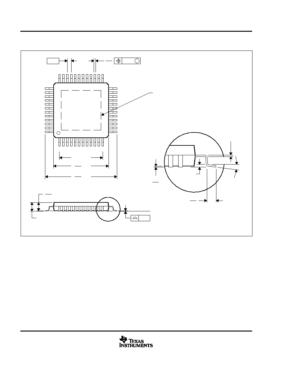
MECHANICAL DATA
PHP (S-PQFP-G48)
PowerPAD
PLASTIC QUAD FLATPACK
Thermal Pad
(see Note D)
Gage Plane
0,13 NOM
0,25
0,45
0,75
Seating Plane
4146927/A 01/98
0,17
0,27
24
25
13
12
SQ
36
37
7,20
6,80
48
1
5,50 TYP
SQ
8,80
9,20
1,05
0,95
1,20 MAX
0,50
M
0,08
0,08
0
∞
≠ 7
∞
0,05
0,15
NOTES: A. All linear dimensions are in millimeters.
B. This drawing is subject to change without notice.
C. Body dimensions do not include mold flash or protrusion.
D. The package thermal performance may be enhanced by bonding the thermal pad to an external thermal plane.
This pad is electrically and thermally connected to the backside of the die and possibly selected leads.
E. Falls within JEDEC MS-026
PowerPAD is a trademark of Texas Instruments Incorporated.

IMPORTANT NOTICE
Texas Instruments Incorporated and its subsidiaries (TI) reserve the right to make corrections, modifications,
enhancements, improvements, and other changes to its products and services at any time and to discontinue
any product or service without notice. Customers should obtain the latest relevant information before placing
orders and should verify that such information is current and complete. All products are sold subject to TI's terms
and conditions of sale supplied at the time of order acknowledgment.
TI warrants performance of its hardware products to the specifications applicable at the time of sale in
accordance with TI's standard warranty. Testing and other quality control techniques are used to the extent TI
deems necessary to support this warranty. Except where mandated by government requirements, testing of all
parameters of each product is not necessarily performed.
TI assumes no liability for applications assistance or customer product design. Customers are responsible for
their products and applications using TI components. To minimize the risks associated with customer products
and applications, customers should provide adequate design and operating safeguards.
TI does not warrant or represent that any license, either express or implied, is granted under any TI patent right,
copyright, mask work right, or other TI intellectual property right relating to any combination, machine, or process
in which TI products or services are used. Information published by TI regarding third≠party products or services
does not constitute a license from TI to use such products or services or a warranty or endorsement thereof.
Use of such information may require a license from a third party under the patents or other intellectual property
of the third party, or a license from TI under the patents or other intellectual property of TI.
Reproduction of information in TI data books or data sheets is permissible only if reproduction is without
alteration and is accompanied by all associated warranties, conditions, limitations, and notices. Reproduction
of this information with alteration is an unfair and deceptive business practice. TI is not responsible or liable for
such altered documentation.
Resale of TI products or services with statements different from or beyond the parameters stated by TI for that
product or service voids all express and any implied warranties for the associated TI product or service and
is an unfair and deceptive business practice. TI is not responsible or liable for any such statements.
Mailing Address:
Texas Instruments
Post Office Box 655303
Dallas, Texas 75265
Copyright
2002, Texas Instruments Incorporated