 | –≠–ª–µ–∫—Ç—Ä–æ–Ω–Ω—ã–π –∫–æ–º–ø–æ–Ω–µ–Ω—Ç: DAC56U | –°–∫–∞—á–∞—Ç—å:  PDF PDF  ZIP ZIP |
Æ
DAC56
1
49%
FPO
Monolithic 16-Bit Resolution
DIGITAL-TO-ANALOG CONVERTER
DAC56
FEATURES
q
COMPLETE D/A CONVERTER:
Internal Voltage Reference
±
3V Output Operational Amplifier
Pinout Allows I
OUT
(
±
1.0mA) Option
No external components required
q
0.012% LINEARITY ERROR MAX
q
12-BIT MONOTONICITY GUARANTEED
OVER 0
∞
C TO +70
∞
C
q
±
5V TO
±
12V POWER SUPPLY
q
SETTLING TIME: V
OUT
= 1.5
µ
s;
I
OUT
= 350ns
q
SERIAL DATA INPUT: Binary Two's
Complement
q
16-PIN PLASTIC DIP AND SOIC
DESCRIPTION
The DAC56 is a complete 16-bit monolithic D/A
converter. Completely self-contained with a stable,
low noise, internal zener voltage reference; high-speed
current switches; a resistor ladder network; and a low
noise output operational amplifier all on a single
monolithic chip. The DAC56 operates over a wide
power supply range from
±
5V to
±
12V.
Differential linearity error (DLE) is guaranteed to
meet specifications without external adjustment. How-
ever, provisions for an externally adjustable circuit
controlling the MSB error, the differential linearity
error at bipolar zero, makes the DLE at BPZ essen-
tially zero and provides for high system performance.
The I/V amplifier stage includes an output current
limiting circuit to protect both amplifier and load from
excessive current. This assures the user of high system
reliability.
A high-speed interface is capable of clocking in data
at a rate of 10MHz max, and its interface logic con-
tains a serial data clock (input), serial data (input) and
latch-enable (input). Serial data is clocked MSB first
into a 16-bit register and then latched into a 16-bit
parallel register.
The DAC56 is packaged in a 16-pin plastic DIP and
16-pin SOIC.
R
F
Output
Reference
16-Bit
I
OUT
DAC
16-Bit Input Latch
16-Bit Serial-to-Parallel Conversion
Clock LE Data
APPLICATIONS
q
PROCESS CONTROL
q
ATE PIN ELECTRONICS LEVEL SETTING
q
CLOSED-LOOP SERVO-CONTROL
q
AUTO-CALIBRATION CIRCUIT FOR A/D
BOARDS
q
UP-GRADE REPLACEMENT FOR
MULTIPLYING D/A
q
X-Y PLOTTER
q
DSP PROCESSOR BOARDS
PDS-1231A
Æ
International Airport Industrial Park ∑ Mailing Address: PO Box 11400, Tucson, AZ 85734 ∑ Street Address: 6730 S. Tucson Blvd., Tucson, AZ 85706 ∑ Tel: (520) 746-1111 ∑ Twx: 910-952-1111
Internet: http://www.burr-brown.com/ ∑ FAXLine: (800) 548-6133 (US/Canada Only) ∑ Cable: BBRCORP ∑ Telex: 066-6491 ∑ FAX: (520) 889-1510 ∑ Immediate Product Info: (800) 548-6132
DAC56
DAC56
SBAS031

Æ
DAC56
2
SPECIFICATIONS
ELECTRICAL
All specifications at +25
∞
C, and power supply voltage of
±
5V, unless otherwise noted.
DAC56
PARAMETER
CONDITIONS
MIN
TYP
MAX
UNITS
DIGITAL INPUT
Resolution
16
Bits
Digital Input Level:
(1)
V
IH
+2.4
+V
L
V
V
IL
0
+0.8
V
I
IH
∑ V
I
= +2.7V
+1
µ
A
I
IL
∑ V
I
= +0.4V
≠50
µ
A
Input Clock Frequency
10
MHz
ACCURACY
Integral Linearity Error
±
0.012
% of FSR
(3)
Differential Linearity Error
±
0.024
% of FSR
Gain Error
±
1.5
% of FSR
Bipolar Zero Error
±
0.5
% of FSR
Monotonicity
0
∞
C to +70
∞
C
12
Bits
TEMPERATURE DRIFT
0
∞
C to +70
∞
C
Gain Drift
±
60
ppm of FSR/
∞
C
Bipolar Zero Drift
±
20
ppm of FSR/
∞
C
Linearity Drift
±
0.012
% of FSR
Differential Linearity Drift
±
0.024
% of FSR
POWER SUPPLY SENSITIVITY
±
V
S
=
±
V
L
=
±
5VDC
Gain
±
0.0045
% of FSR/%V
Bipolar Zero
±
0.0015
% of FSR/%V
SETTLING TIME
to
±
0.006% of FSR
Voltage Output
6V Step
1.5
µ
s
1LSB
1
µ
s
Current Output
1mA Step
10 to 100
Load
350
ns
1k
Load
(3)
350
ns
Slew Rate
12
V/
µ
s
ANALOG OUTPUT
Voltage Output Configuration
Bipolar Range
±
2.66
±
3.0
±
3.34
V
Output Current
±
8
mA
Output Impedance
0.1
Short Circuit Duration
Indefinite to Common
Current Output Configuration
Bipolar Range
±
1
mA
Output Impedance
1.2
k
WARMUP TIME
1
min
POWER SUPPLY REQUIREMENTS
(4)
Supply Voltage
+V
S
and +V
L
+4.75
+5.00
+13.2
V
≠V
S
and ≠V
L
≠4.75
≠5.00
≠13.2
V
Supply Drain (No Load)
+V (+V
S
and +V
L
= +5V)
+10
+17
mA
≠V (≠V
S
and ≠V
L
= ≠5V)
≠25
≠35
mA
+V (+V
S
and +V
L
= +12V)
+12
mA
≠V (≠V
S
and ≠V
L
= ≠12V)
≠27
mA
Power Dissipation
V
S
and V
L
=
±
5V
175
260
mW
V
S
and V
L
=
±
12V
468
mW
TEMPERATURE RANGE
Specification
0
70
∞
C
Storage
≠60
100
∞
C
NOTES: (1) Logic input levels are TTL-/CMOS-compatible. (2) FSR means full-scale range and is equivalent to 6V (
±
3V) for DAC56 in the V
OUT
mode. (3) Measured
with an active clamp to provide a low impedance for approximately 200ns. (4) All specifications assume +V
S
connected to +V
L
and ≠V
S
connected to ≠V
L
. If supplies
are connected separately, ≠V
L
must not be more negative than ≠V
S
to assure proper operation. No similar restriction applies to the value of +V
L
with respect to +V
S
.

Æ
DAC56
3
PIN CONFIGURATION
PIN
NAME
FUNCTION
1
≠V
S
Analog Negative Supply
2
LCOM
Logic Common
3
+V
L
Logic Positive Supply
4
NC
No Connection
5
CLK
Clock Input
6
LE
Latch Enable Input
7
DATA
Serial Data Input
8
≠V
L
Logic Negative Supply
9
V
OUT
Voltage Output
10
R
F
Feedback Resistor
11
SJ
Summing Junction
12
ACOM
Analog Common
13
I
OUT
Current Output
14
MSB ADJ
MSB Adjustment Terminal
15
TRIM
MSB Trim-pot Terminal
16
+V
S
Analog Positive Supply
PIN ASSIGNMENTS
ABSOLUTE MAXIMUM RATINGS
DC Supply Voltage .......................................................................
±
15VDC
Input Logic Voltage ........................................................... ≠1V to +V
S
/+V
L
Power Dissipation .......................................................................... 850mW
Operating Temperature ................................................... ≠25
∞
C to +70
∞
C
Storage Temperature ..................................................... ≠80
∞
C to +100
∞
C
Lead Temperature (soldering, 10s) ............................................... +300
∞
C
The information provided herein is believed to be reliable; however, BURR-BROWN assumes no responsibility for inaccuracies or omissions. BURR-BROWN assumes
no responsibility for the use of this information, and all use of such information shall be entirely at the user's own risk. Prices and specifications are subject to change
without notice. No patent rights or licenses to any of the circuits described herein are implied or granted to any third party. BURR-BROWN does not authorize or warrant
any BURR-BROWN product for use in life support devices and/or systems.
ELECTROSTATIC
DISCHARGE SENSITIVITY
Electrostatic discharge can cause damage ranging from per-
formance degradation to complete device failure. Burr-
Brown Corporation recommends that all integrated circuits
be handled and stored using appropriate ESD protection
methods.
PACKAGE INFORMATION
PACKAGE DRAWING
PRODUCT
PACKAGE
NUMBER
(1)
DAC56P
16-Pin Plastic DIP
180
DAC56U
16-Pin SOIC
211
NOTE: (1) For detailed drawing and dimension table, please see end of data
sheet, or Appendix C of Burr-Brown IC Data Book.
16-Bit
DAC Latch
16-Bit Serial
to Parallel
Conversion
Control
Logic and
Level
Shifting
Circuit
1
2
3
4
5
6
7
8
16
15
14
13
12
11
10
9
16-Bit
I
OUT
DAC
≠5V
+5V
≠5V
1µF
1µF
1µF
LCOM
≠V
S
+V
L
NC
CLK
LE
Data
≠V
L
+V
S
SJ
R
F
V
OUT
(±3.0V)
TRIM
MSB ADJ
I
OUT
Analog
Output
1µF
+5V
ACOM
NOTES:
= Analog Common
= Logic Common
Æ
DAC56
4
OPERATING INSTRUCTIONS
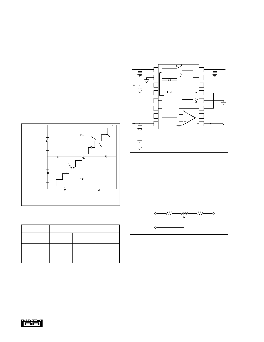
The accuracy of a D/A converter is described by the transfer
function as shown in Figure 1. Digital input to analog output
converter relationships are shown in Table I. The errors in
the D/A converter are combinations of analog errors due to
the linear circuitry, matching and tracking properties of the
ladder and scaling networks, power supply rejection, and
reference errors. In summary, these errors consist of initial
errors including gain, offset, linearity, differential linearity,
and power supply sensitivity. Gain drift over temperature
rotates the line (Figure 1) about the bipolar zero point and
offset drift shifts the line left or right over the operating
temperature range. Most of the offset and gain drift is due to
the drift of the internal reference zener diode with tempera-
ture or time.
The converter is designed so that these drifts are in opposite
directions. This way the bipolar zero voltage is virtually
unaffected by variations in the reference voltage.
DIGITAL INPUT CODES
The DAC56 accepts serial input data (MSB first) in Binary
Two's Complement form--Refer to Table I for input/output
relationships.
POWER SUPPLY CONNECTIONS
Power supply decoupling capacitors should be added as
shown in the Connection Diagram (Figure 2), for optimum
performance and noise rejection.
These capacitors (1
µ
F tantalum recommended) should be
connected as close as possible to the converter.
FIGURE 2. Connection Diagram.
MSB ERROR ADJUSTMENT (OPTIONAL)
Differential linearity error at all codes of the DAC56 is
guaranteed to meet specifications without an external adjust-
ment. However, if adjustment of the differential linearity
error at bipolar zero is desired, it can be trimmed essentially
to zero using the circuit as shown in Figure 3.
FIGURE 3. MSB Adjustment Circuit.
After allowing ample warm-up time (5 to 10 minutes) to
assure stable operation, select the input code FFFF
H
. Mea-
sure the output voltage using a 6-1/2 digit voltmeter and
record the measurement. Change the digital input code to
0000
H
. Adjust the 100k
potentiometer (TCR of 100ppm
per
∞
C or less is recommended) to make the output voltage
read 1LSB more than the voltage reading of the previous
code (ex. 1LSB = 92
µ
V at FSR = 6V).
If the MSB adjustment circuit is not used, pins 14 and 15
should be left open.
FIGURE 1. Input vs Output for an Ideal Bipolar D/A
Converter.
DIGITAL INPUT
ANALOG OUTPUT
Binary Two's
Voltage (V),
Current (mA),
Complement (BTC)
DAC Output
V
OUT
Mode
I
OUT
Mode
7FFF
H
+ Full Scale
+2.999908
≠0.999970
8000
H
≠ Full Scale
≠3.000000
+1.000000
0000
H
Bipolar Zero
0.000000
0.000000
FFFF
H
Zero ≠1LSB
≠0.000092
+0.030500
µ
A
TABLE I. Digital Input to Analog Output Relationship.
470k
200k
100k
(1)
Trim 15
MSB Adjust 14
1 ≠V
S
NOTE: (1) 10-15 turns.
Gain
Drift
Offset
Drift
Bipolar
Zero
0111...1111
1000...0000
Analog Input
Digital Output
(+FSR/2) ≠1LSB
≠FSR/2
All Bits
On
* See Table I for digital code definitions.
16-Bit
DAC Latch
16-Bit Serial
to Parallel
Conversion
Control
Logic and
Level
Shifting
Circuit
1
2
3
4
5
6
7
8
16
15
14
13
12
11
10
9
16-Bit
I
OUT
DAC
≠5V
+5V
≠5V
1µF
1µF
1µF
LCOM
≠V
S
+V
L
NC
CLK
LE
Data
≠V
L
+V
S
SJ
R
F
V
OUT
(±3.0V)
TRIM
MSB ADJ
I
OUT
Analog
Output
1µF
+5V
ACOM
NOTES:
= Analog Common
= Logic Common

Æ
DAC56
5
FIGURE 4. Input Timing Diagram.
INPUT TIMING CONSIDERATIONS
Figures 4 and 5 refer to the input timing required to interface
the inputs of DAC56 to a serial input data stream. Serial data
is accepted in Binary Two's Complement with the MSB being
loaded first. Data is clocked in on positive going clock (CLK,
pin 5) edges and is latched into the DAC input register on
negative going latch enable (LE, pin 6) edges.
The latch enable input must be high for at least one clock cycle
before going low, and then must be held low for at least one
clock cycle. The last 16 data bits clocked into the serial input
register are those that are transferred to the DAC input register
when latch enable goes low. In other words, when more than
16 clock cycles occur between a latch enable, only the data
present during the last 16 clocks will be transferred to the
DAC input register.
Figure 4 gives the general input format required for the
DAC56. Figure 5 shows the specific relationships between the
various signals and their timing constraints.
FIGURE 5. Input Timing Relationships.
MSB
DATA
> 40ns
> One Clock Cycle
LE
> One Clock Cycle
CLK
> 40ns
> 5ns
> 100ns
LSB
>15ns >15ns
> 40ns
> 15ns
DATA
LE
2
(2)
CLK
(3)
MSB
LSB
MSB
(4)
(1)
NOTES: (1) If clock is stopped between input of 16-bit data words, latch enable (LE) must remain low until after the first clock of the next 16-bit data
word stream. (2) Data format is binary two's complement (BTC). Individual data bits are clocked in on the corresponding positive clock edge. (3) Latch
enable (LE) must remain low at least one clock cycle after going negative. (4) Latch enable (LE) must be high for at least one clock cycle before going
negative.
1
16
15
14
13
12
11
10
9
8
7
6
5
4
3
2
1

PACKAGING INFORMATION
ORDERABLE DEVICE
STATUS(1)
PACKAGE TYPE
PACKAGE DRAWING
PINS
PACKAGE QTY
DAC56P
OBSOLETE
PDIP
N
16
DAC56U
OBSOLETE
CDIP SB
JVF
16
DAC56U/1K
OBSOLETE
CDIP SB
JVF
16
(1) The marketing status values are defined as follows:
ACTIVE: Product device recommended for new designs.
LIFEBUY: TI has announced that the device will be discontinued, and a lifetime-buy period is in effect.
NRND: Not recommended for new designs. Device is in production to support existing customers, but TI does not recommend using this part in
a new design.
PREVIEW: Device has been announced but is not in production. Samples may or may not be available.
OBSOLETE: TI has discontinued the production of the device.
PACKAGE OPTION ADDENDUM
www.ti.com
3-Oct-2003

IMPORTANT NOTICE
Texas Instruments Incorporated and its subsidiaries (TI) reserve the right to make corrections, modifications,
enhancements, improvements, and other changes to its products and services at any time and to discontinue
any product or service without notice. Customers should obtain the latest relevant information before placing
orders and should verify that such information is current and complete. All products are sold subject to TI's terms
and conditions of sale supplied at the time of order acknowledgment.
TI warrants performance of its hardware products to the specifications applicable at the time of sale in
accordance with TI's standard warranty. Testing and other quality control techniques are used to the extent TI
deems necessary to support this warranty. Except where mandated by government requirements, testing of all
parameters of each product is not necessarily performed.
TI assumes no liability for applications assistance or customer product design. Customers are responsible for
their products and applications using TI components. To minimize the risks associated with customer products
and applications, customers should provide adequate design and operating safeguards.
TI does not warrant or represent that any license, either express or implied, is granted under any TI patent right,
copyright, mask work right, or other TI intellectual property right relating to any combination, machine, or process
in which TI products or services are used. Information published by TI regarding third-party products or services
does not constitute a license from TI to use such products or services or a warranty or endorsement thereof.
Use of such information may require a license from a third party under the patents or other intellectual property
of the third party, or a license from TI under the patents or other intellectual property of TI.
Reproduction of information in TI data books or data sheets is permissible only if reproduction is without
alteration and is accompanied by all associated warranties, conditions, limitations, and notices. Reproduction
of this information with alteration is an unfair and deceptive business practice. TI is not responsible or liable for
such altered documentation.
Resale of TI products or services with statements different from or beyond the parameters stated by TI for that
product or service voids all express and any implied warranties for the associated TI product or service and
is an unfair and deceptive business practice. TI is not responsible or liable for any such statements.
Following are URLs where you can obtain information on other Texas Instruments products and application
solutions:
Products
Applications
Amplifiers
amplifier.ti.com
Audio
www.ti.com/audio
Data Converters
dataconverter.ti.com
Automotive
www.ti.com/automotive
DSP
dsp.ti.com
Broadband
www.ti.com/broadband
Interface
interface.ti.com
Digital Control
www.ti.com/digitalcontrol
Logic
logic.ti.com
Military
www.ti.com/military
Power Mgmt
power.ti.com
Optical Networking
www.ti.com/opticalnetwork
Microcontrollers
microcontroller.ti.com
Security
www.ti.com/security
Telephony
www.ti.com/telephony
Video & Imaging
www.ti.com/video
Wireless
www.ti.com/wireless
Mailing Address:
Texas Instruments
Post Office Box 655303 Dallas, Texas 75265
Copyright
2003, Texas Instruments Incorporated