APPLICATIONS
q
PORTABLE BATTERY-POWERED
INSTRUMENTS
q
DIGITAL GAIN AND OFFSET
ADJUSTMENT
q
PROGRAMMABLE VOLTAGE AND
CURRENT SOURCES
Low-Power, Rail-to-Rail Output, 12-Bit Serial Input
DIGITAL-TO-ANALOG CONVERTER
DESCRIPTION
The DAC7512 is a low-power, single, 12-bit buffered voltage
output Digital-to-Analog Converter (DAC). Its on-chip preci-
sion output amplifier allows rail-to-rail output swing to be
achieved. The DAC7512 uses a versatile three-wire serial
interface that operates at clock rates up to 30MHz and is
compatible with standard SPI
TM
, QSPI
TM
, Microwire
TM
, and
DSP interfaces.
The reference for the DAC7512 is derived from the power
supply, resulting in the widest dynamic output range possible.
The DAC7512 incorporates a power-on reset circuit that
ensures that the DAC output powers up at 0V and remains
there until a valid write takes place in the device. The
DAC7512 contains a power-down feature, accessed over the
serial interface, that can reduce the current consumption of
the device to 50nA at 5V.
The low power consumption of this part in normal operation
makes it ideally suited to portable battery-operated equip-
ment. The power consumption is 0.7mW at 5V reducing to
1�W in power-down mode.
The DAC7512 is available in a SOT23-6 package and an
MSOP-8 package.
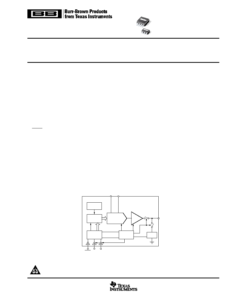
DAC7512
DAC7512
FEATURES
q
microPOWER OPERATION: 135�A at 5V
q
POWER-DOWN: 200nA at 5V, 50nA at 3V
q
POWER SUPPLY: +2.7V to +5.5V
q
TESTED MONOTONIC BY DESIGN
q
POWER-ON RESET TO 0V
q
THREE POWER-DOWN FUNCTIONS
q
LOW POWER SERIAL INTERFACE WITH
SCHMITT-TRIGGERED INPUTS
q
ON-CHIP OUTPUT BUFFER AMPLIFIER,
RAIL-TO-RAIL OPERATION
q
SYNC INTERRUPT FACILITY
q
SOT23-6 AND MSOP-8 PACKAGES
Power-On
Reset
DAC
Register
REF (+) REF (�)
12-Bit
DAC
Output
Buffer
Input
Control
Logic
Power-Down
Control Logic
Resistor
Network
SYNC SCLK D
IN
V
DD
GND
V
OUT
SPI and QSPI are registered trademarks of Motorola.
Microwire is a registered trademark of National Semiconductor.
DAC7512
SBAS156B � JULY 2002
www.ti.com
PRODUCTION DATA information is current as of publication date.
Products conform to specifications per the terms of Texas Instruments
standard warranty. Production processing does not necessarily include
testing of all parameters.
Copyright � 2002, Texas Instruments Incorporated
Please be aware that an important notice concerning availability, standard warranty, and use in critical applications of
Texas Instruments semiconductor products and disclaimers thereto appears at the end of this data sheet.
DAC7512
2
SBAS156B
www.ti.com
V
DD
to GND ........................................................................... �0.3V to +6V
Digital Input Voltage to GND .................................. �0.3V to +V
DD
+ 0.3V
V
OUT
to GND ........................................................... �0.3V to +V
DD
+ 0.3V
Operating Temperature Range ..................................... �40�C to +105�C
Storage Temperature Range ......................................... �65�C to +150�C
Junction Temperature Range (T
J
max) ......................................... +150�C
SOT23 Package:
Power Dissipation .................................................. (T
J
max -- T
A
)/
JA
JA
Thermal Impedance ......................................................... 240�C/W
Lead Temperature, Soldering:
Vapor Phase (60s) ............................................................... +215�C
Infrared (15s) ........................................................................ +220�C
MSOP Package:
Power Dissipation ........................................................ (T
J
max -- T
A
)/
JA
JA
Thermal Impedance ......................................................... 206�C/W
JC
Thermal Impedance ........................................................... 44�C/W
Lead Temperature, Soldering:
Vapor Phase (60s) ............................................................... +215�C
Infrared (15s) ........................................................................ +220�C
NOTE: (1) Stresses above those listed under "Absolute Maximum Ratings"
may cause permanent damage to the device. Exposure to absolute maximum
conditions for extended periods may affect device reliability.
ELECTROSTATIC
DISCHARGE SENSITIVITY
This integrated circuit can be damaged by ESD. Texas Instru-
ments recommends that all integrated circuits be handled with
appropriate precautions. Failure to observe proper handling
and installation procedures can cause damage.
ESD damage can range from subtle performance degradation
to complete device failure. Precision integrated circuits may be
more susceptible to damage because very small parametric
changes could cause the device not to meet its published
specifications.
ABSOLUTE MAXIMUM RATINGS
(1)
PACKAGE/ORDERING INFORMATION
MINIMUM
RELATIVE
DIFFERENTIAL
SPECIFIED
ACCURACY
NONLINEARITY
PACKAGE
TEMPERATURE
PACKAGE
ORDERING
TRANSPORT
PRODUCT
(LSB)
(LSB)
PACKAGE-LEAD
DESIGNATOR
(1)
RANGE
MARKING
NUMBER
(1)
MEDIA, QUANTITY
DAC7512E
�8
�1
MSOP-8
DGK
�40�C to +105�C
D12E
DAC7512E/250
Tape and Reel, 250
"
"
"
"
"
"
"
DAC7512E/2K5
Tape and Reel, 2500
DAC7512N
�8
�1
SOT23-6
DBV
�40�C to +105�C
D12N
DAC7512N/250
Tape and Reel, 250
"
"
"
"
"
"
"
DAC7512N/3K
Tape and Reel, 3000
NOTES: (1) For the most current specifications and package information, refer to our web site at www.ti.com. (2) Models with a slash (/) are available only in Tape
and Reel in the quantities indicated (e.g., /2K5 indicates 2500 devices per reel). Ordering 2500 pieces of "DAC7512E/2K5" will get a single 2500-piece Tape and Reel.
PIN
NAME
DESCRIPTION
1
V
OUT
Analog output voltage from DAC. The output ampli-
fier has rail-to-rail operation.
2
GND
Ground reference point for all circuitry on the part.
3
V
DD
Power Supply Input, +2.7V to 5.5V.
4
D
IN
Serial Data Input. Data is clocked into the 16-bit
input shift register on the falling edge of the serial
clock input.
5
SCLK
Serial Clock Input. Data can be transferred at rates
up to 30MHz.
6
SYNC
Level triggered control input (active LOW). This is
the frame sychronization signal for the input data.
When SYNC goes LOW, it enables the input shift
register and data is transferred in on the falling
edges of the following clocks. The DAC is updated
following the 16th clock cycle unless SYNC is taken
HIGH before this edge, in which case the rising
edge of SYNC acts as an interrupt and the write
sequence is ignored by the DAC7512.
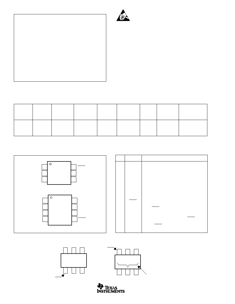
PIN DESCRIPTION (SOT23-6)
PIN CONFIGURATIONS
Top View
SOT23-6
MSOP-8
V
DD
NC
NC
V
OUT
GND
D
IN
SCLK
SYNC
1
2
3
4
8
7
6
5
DAC7512
NC = No Internal Connection
V
OUT
GND
V
DD
SYNC
SCLK
D
IN
1
2
3
6
5
4
DAC7512
DAC7512N LOT TRACE LOCATION
Pin 1
D12N
Top View
Pin 1
YMLL
Bottom View
Lot Trace Code

DAC7512
3
SBAS156B
www.ti.com
PARAMETER
CONDITIONS
MIN
TYP
MAX
UNITS
STATIC PERFORMANCE
(1)
Resolution
12
Bits
Relative Accuracy
�8
LSB
Differential Nonlinearity
Tested Monotonic by Design
�1
LSB
Zero Code Error
All Zeroes Loaded to DAC Register
+5
+20
mV
Full-Scale Error
All Ones Loaded to DAC Register
�0.15
�1.25
% of FSR
Gain Error
�1.25
% of FSR
Zero Code Error Drift
�20
�V/�C
Gain Temperature Coefficient
�5
ppm of FSR/�C
OUTPUT CHARACTERISTICS
(2)
Output Voltage Range
0
V
DD
V
Output Voltage Settling Time
1/4 Scale to 3/4 Scale Change
(400
H
to C00
H
)
8
10
�s
R
L
= 2k
; 0pF < C
L
< 200pF
R
L
= 2k
; C
L
= 500pF
12
�s
Slew Rate
1
V/�s
Capacitive Load Stability
R
L
= �
470
pF
R
L
= 2k
1000
pF
Code Change Glitch Impulse
1LSB Change Around Major Carry
20
nV-s
Digital Feedthrough
0.5
nV-s
DC Output Impedance
1
Short-Circuit Current
V
DD
= +5V
50
mA
V
DD
= +3V
20
mA
Power-Up Time
Coming Out of Power-Down Mode
V
DD
= +5V
2.5
�s
Coming Out of Power-Down Mode
V
DD
= +3V
5
�s
LOGIC INPUTS
(2)
Input Current
�1
�A
V
IN
L, Input Low Voltage
V
DD
= +5V
0.8
V
V
IN
L, Input Low Voltage
V
DD
= +3V
0.6
V
V
IN
H, Input High Voltage
V
DD
= +5V
2.4
V
V
IN
H, Input High Voltage
V
DD
= +3V
2.1
V
Pin Capacitance
3
pF
POWER REQUIREMENTS
V
DD
2.7
5.5
V
I
DD
(normal mode)
DAC Active and Excluding Load Current
V
DD
= +3.6V to +5.5V
V
IH
= V
DD
and V
IL
= GND
135
200
�A
V
DD
= +2.7V to +3.6V
V
IH
= V
DD
and V
IL
= GND
115
160
�A
I
DD
(all power-down modes)
V
DD
= +3.6V to +5.5V
V
IH
= V
DD
and V
IL
= GND
0.2
1
�A
V
DD
= +2.7V to +3.6V
V
IH
= V
DD
and V
IL
= GND
0.05
1
�A
POWER EFFICIENCY
I
OUT
/I
DD
I
LOAD
= 2mA. V
DD
= +5V
93
%
TEMPERATURE RANGE
Specified Performance
�40
+105
�C
NOTES: (1) Linearity calculated using a reduced code range of 48 to 4047; output unloaded. (2) Guaranteed by design and characterization, not production tested.
ELECTRICAL CHARACTERISTICS
V
DD
= +2.7V to +5.5V; R
L
= 2k� to GND; C
L
= 200pF to GND.
DAC7512E, N
DAC7512
4
SBAS156B
www.ti.com
PARAMETER
DESCRIPTION
CONDITIONS
MIN
TYP
MAX
UNITS
t
1
(3)
SCLK Cycle Time
V
DD
= 2.7V to 3.6V
50
ns
V
DD
= 3.6V to 5.5V
33
ns
t
2
SCLK HIGH Time
V
DD
= 2.7V to 3.6V
13
ns
V
DD
= 3.6V to 5.5V
13
ns
t
3
SCLK LOW Time
V
DD
= 2.7V to 3.6V
22.5
ns
V
DD
= 3.6V to 5.5V
13
ns
t
4
SYNC to SCLK Rising
Edge Setup Time
V
DD
= 2.7V to 3.6V
0
ns
V
DD
= 3.6V to 5.5V
0
ns
t
5
Data Setup Time
V
DD
= 2.7V to 3.6V
5
ns
V
DD
= 3.6V to 5.5V
5
ns
t
6
Data Hold Time
V
DD
= 2.7V to 3.6V
4.5
ns
V
DD
= 3.6V to 5.5V
4.5
ns
t
7
SCLK Falling Edge to
SYNC Rising Edge
V
DD
= 2.7V to 3.6V
0
ns
V
DD
= 3.6V to 5.5V
0
ns
t
8
Minimum SYNC HIGH Time
V
DD
= 2.7V to 3.6V
50
ns
V
DD
= 3.6V to 5.5V
33
ns
NOTES: (1) All input signals are specified with t
R
= t
F
= 5ns (10% to 90% of V
DD
) and timed from a voltage level of (V
IL
+ V
IH
)/2. (2) See Serial Write Operation timing
diagram, below. (3) Maximum SCLK frequency is 30MHz at V
DD
= +3.6V to +5.5V and 20MHz at V
DD
= +2.7V to +3.6V.
TIMING CHARACTERISTICS
(1, 2)
V
DD
= +2.7V to +5.5V; all specifications �40�C to +105�C, unless otherwise noted.
DAC7512E, N
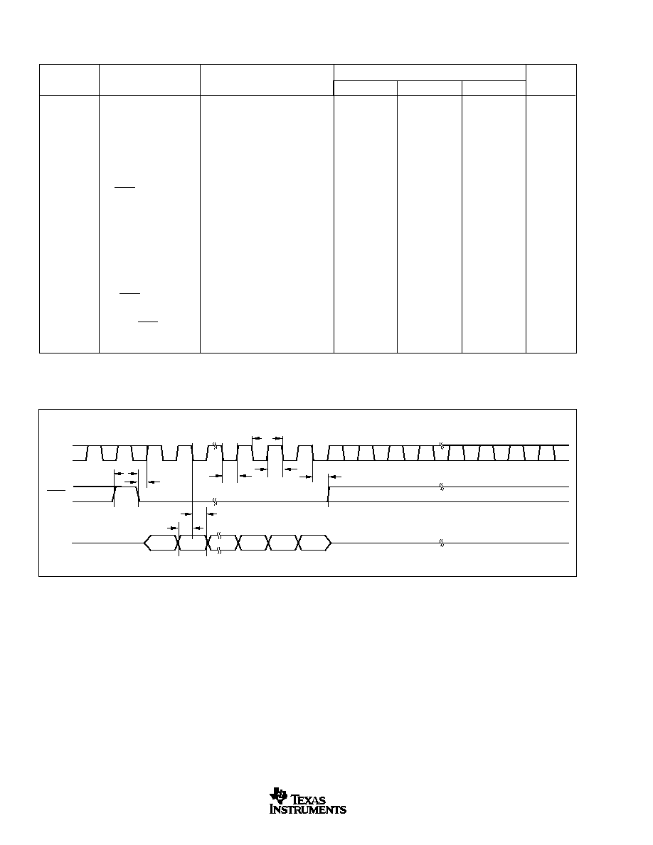
SERIAL WRITE OPERATION
SCLK
SYNC
D
IN
DB15
DB0
t
8
t
3
t
2
t
7
t
4
t
5
t
6
t
1
DAC7512
5
SBAS156B
www.ti.com
TYPICAL CHARACTERISTICS: V
DD
= +5V
At T
A
= +25�C, +V
DD
= +5V, unless otherwise noted.
ZERO-SCALE ERROR vs TEMPERATURE
�40
Error (mV)
Temperature (
�
C)
0
40
80
120
30
20
10
0
�10
�20
�30
FULL-SCALE ERROR vs TEMPERATURE
�40
Error (mV)
Temperature (
�
C)
0
40
80
120
30
20
10
0
�10
�20
�30
TYPICAL TOTAL UNADJUSTED ERROR
0
TUE (LSBs)
CODE
200
H
400
H
600
H
800
H
A00
H
C00
H
E00
H
FFF
H
16
8
0
�8
�16
16.0
12.0
8.0
4.0
0.0
�4.0
�8.0
�12.0
�16.0
LE (LSB)
LINEARITY ERROR AND
DIFFERENTIAL LINEARITY ERROR vs CODE
(�40
�
C)
0
200
H
400
H
600
H
800
H
CODE
A00
H
C00
H
E00
H
FFF
H
1.0
0.5
0.0
�0.5
�1.0
DLE (LSB)
16.0
12.0
8.0
4.0
0.0
�4.0
�8.0
�12.0
�16.0
LE (LSB)
LINEARITY ERROR AND
DIFFERENTIAL LINEARITY ERROR vs CODE
(+25
�
C)
0
200
H
400
H
600
H
800
H
CODE
A00
H
C00
H
E00
H
FFF
H
1.0
0.5
0.0
�0.5
�1.0
DLE (LSB)
16.0
12.0
8.0
4.0
0.0
�4.0
�8.0
�12.0
�16.0
LE (LSB)
LINEARITY ERROR AND
DIFFERENTIAL LINEARITY ERROR vs CODE
(+105
�
C)
0
200
H
400
H
600
H
800
H
CODE
A00
H
C00
H
E00
H
FFF
H
1.0
0.5
0.0
�0.5
�1.0
DLE (LSB)

DAC7512
6
SBAS156B
www.ti.com
TYPICAL CHARACTERISTICS: V
DD
= +5V
(Cont.)
At T
A
= +25�C, +V
DD
= +5V, unless otherwise noted.
SOURCE AND SINK CURRENT CAPABILITY
0
V
OUT
(V)
I
SOURCE/SINK
(mA)
5
10
15
5
4
3
2
1
0
DAC Loaded with FFF
H
DAC Loaded with 000
H
SUPPLY CURRENT vs CODE
0
I
DD
(
�
A)
CODE
200
H
400
H
600
H
800
H
A00
H
C00
H
E00
H
FFF
H
500
400
300
200
100
0
SUPPLY CURRENT vs TEMPERATURE
�40
I
DD
(
�
A)
Temperature (
�
C)
0
40
80
120
300
250
200
150
100
50
0
SUPPLY CURRENT vs SUPPLY VOLTAGE
2.7
I
DD
(
�
A)
V
DD
(V)
3.2
3.7
4.2
4.7
5.2
5.7
300
250
200
150
100
50
0
I
DD
HISTOGRAM
Frequency
I
DD
(
�
A)
3000
2500
2000
1500
1000
500
0
50
60
70
80
90
100
110
120
130
140
150
160
170
180
190
POWER-DOWN CURRENT vs SUPPLY VOLTAGE
2.7
I
DD
(nA)
V
DD
(V)
3.2
3.7
4.2
4.7
5.2
5.7
100
90
80
70
60
50
40
30
20
10
0
+25
�
C
�40
�
C
+105
�
C

DAC7512
7
SBAS156B
www.ti.com
TYPICAL CHARACTERISTICS: V
DD
= +5V
(Cont.)
At T
A
= +25�C, +V
DD
= +5V, unless otherwise noted.
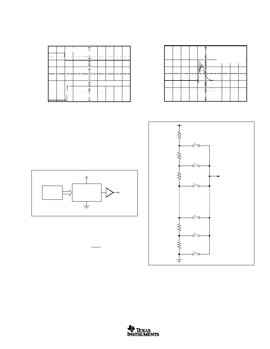
POWER-ON RESET TO 0V
Time (20
�
s/div)
Loaded with 2k
to V
DD
.
V
DD
(1V/div)
V
OUT
(1V/div)
HALF-SCALE SETTLING TIME
Time (1
�
s/div)
CLK (5V/div)
V
OUT
(1V/div)
Half-Scale Code Change
C00
H
to 400
H
Output Loaded with
2k
and 200pF to GND
HALF-SCALE SETTLING TIME
Time (1
�
s/div)
CLK (5V/div)
V
OUT
(1V/div)
Half-Scale Code Change
400
H
to C00
H
Output Loaded with
2k
and 200pF to GND
FULL-SCALE SETTLING TIME
Time (1
�
s/div)
CLK (5V/div)
V
OUT
(1V/div)
Full-Scale Code Change
FFF
H
to 000
H
Output Loaded with
2k
and 200pF to GND
FULL-SCALE SETTLING TIME
CLK (5V/div)
V
OUT
(1V/div)
Time (1
�
s/div)
Full-Scale Code Change
000
H
to FFF
H
Output Loaded with
2k
and 200pF to GND
SUPPLY CURRENT vs LOGIC INPUT VOLTAGE
0
I
DD
(
�
A)
V
LOGIC
(V)
1
2
3
4
5
2500
2000
1500
1000
500
0

DAC7512
8
SBAS156B
www.ti.com
TYPICAL TOTAL UNADJUSTED ERROR
0
TUE (LSBs)
CODE
200
H
400
H
600
H
800
H
A00
H
C00
H
E00
H
FFF
H
16
8
0
�8
�16
16.0
12.0
8.0
4.0
0.0
�4.0
�8.0
�12.0
�16.0
LE (LSB)
LINEARITY ERROR AND
DIFFERENTIAL LINEARITY ERROR vs CODE
(�40
�
C)
0
200
H
400
H
600
H
800
H
CODE
A00
H
C00
H
E00
H
FFF
H
1.0
0.5
0.0
�0.5
�1.0
DLE (LSB)
16.0
12.0
8.0
4.0
0.0
�4.0
�8.0
�12.0
�16.0
LE (LSB)
LINEARITY ERROR AND
DIFFERENTIAL LINEARITY ERROR vs CODE
(+25
�
C)
0
200
H
400
H
600
H
800
H
CODE
A00
H
C00
H
E00
H
FFF
H
1.0
0.5
0.0
�0.5
�1.0
DLE (LSB)
16
12
8
4
0
�4
�8
�12
�16
LE (LSB)
LINEARITY ERROR AND
DIFFERENTIAL LINEARITY ERROR vs CODE
(+105
�
C)
000
H
200
H
400
H
600
H
800
H
CODE
A00
H
C00
H
E00
H
FFF
H
1.0
0.5
0
�0.5
�1.0
DLE (LSB)
TYPICAL CHARACTERISTICS: V
DD
= +5V
(Cont.)
At T
A
= +25�C, +V
DD
= +5V, unless otherwise noted.
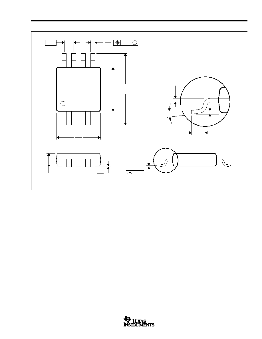
EXITING POWER-DOWN
(800
H
Loaded)
Time (5
�
s/div)
CLK (5V/div)
V
OUT
(1V/div)
CODE CHANGE GLITCH
Time (0.5
�
s/div)
Loaded with 2k
and 200pF to GND.
Code Change:
800
H
to 7FF
H
.
V
OUT
(20mV/div)
TYPICAL CHARACTERISTICS: V
DD
= +2.7V
At T
A
= +25�C, +V
DD
= +2.7V, unless otherwise noted.

DAC7512
9
SBAS156B
www.ti.com
TYPICAL CHARACTERISTICS: V
DD
= +2.7V
(Cont.)
At T
A
= +25�C, +V
DD
= +2.7V, unless otherwise noted.
FULL-SCALE ERROR vs TEMPERATURE
�40
Error (mV)
Temperature (
�
C)
0
40
80
120
30
20
10
0
�10
�20
�30
ZERO-SCALE ERROR vs TEMPERATURE
�40
Error (mV)
Temperature (
�
C)
0
40
80
120
30
20
10
0
�10
�20
�30
SOURCE AND SINK CURRENT CAPABILITY
0
V
OUT
(V)
I
SOURCE/SINK
(mA)
5
10
15
3
2
1
0
DAC Loaded with FFF
H
DAC Loaded with 000
H
V
DD
= +3V
500
400
300
200
100
0
SUPPLY CURRENT vs CODE
0
I
DD
(
�
A)
CODE
200
H
400
H
600
H
800
H
A00
H
C00
H
E00
H
FFF
H
SUPPLY CURRENT vs TEMPERATURE
�40
I
DD
(
�
A)
Temperature (
�
C)
0
40
80
120
300
250
200
150
100
50
0
I
DD
HISTOGRAM
Frequency
I
DD
(
�
A)
3000
2500
2000
1500
1000
500
0
50
60
70
80
90
100
110
120
130
140
150
160
170
180
190
V
REF
tied to V
DD
.

DAC7512
10
SBAS156B
www.ti.com
FULL-SCALE SETTLING TIME
Time (1
�
s/div)
CLK (2.7V/div)
V
OUT
(1V/div)
Full-Scale Code Change
FFF
H
to 000
H
Output Loaded with
2k
and 200pF to GND
HALF-SCALE SETTLING TIME
Time (1
�
s/div)
CLK (2.7V/div)
V
OUT
(1V/div)
Half-Scale Code Change
400
H
to C00
H
Output Loaded with
2k
and 200pF to GND
HALF-SCALE SETTLING TIME
Time (1
�
s/div)
CLK (2.7V/div)
V
OUT
(1V/div)
Half-Scale Code Change
C00
H
to 400
H
Output Loaded with
2k
and 200pF to GND
POWER-ON RESET to 0V
Time (20
�
s/div)
TYPICAL CHARACTERISTICS: V
DD
= +2.7V
(Cont.)
At T
A
= +25�C, +V
DD
= +2.7V, unless otherwise noted.
SUPPLY CURRENT vs LOGIC INPUT VOLTAGE
0
I
DD
(
�
A)
V
LOGIC
(V)
1
2
3
4
5
2500
2000
1500
1000
500
0
FULL-SCALE SETTLING TIME
Time (1
�
s/div)
CLK (2.7V/div)
V
OUT
(1V/div)
Full-Scale Code Change
000
H
to FFF
H
Output Loaded with
2k
and 200pF to GND
DAC7512
11
SBAS156B
www.ti.com
TYPICAL CHARACTERISTICS: V
DD
= +2.7V
(Cont.)
At T
A
= +25�C, +V
DD
= +2.7V, unless otherwise noted.
EXITING POWER-DOWN
(800
H
Loaded)
Time (5
�
s/div)
CLK (2.7V/div)
V
OUT
(1V/div)
CODE CHANGE GLITCH
Time (0.5
�
s/div)
Loaded with 2k
and 200pF to GND.
Code Change:
800
H
to 7FF
H
.
V
OUT
(20mV/div)
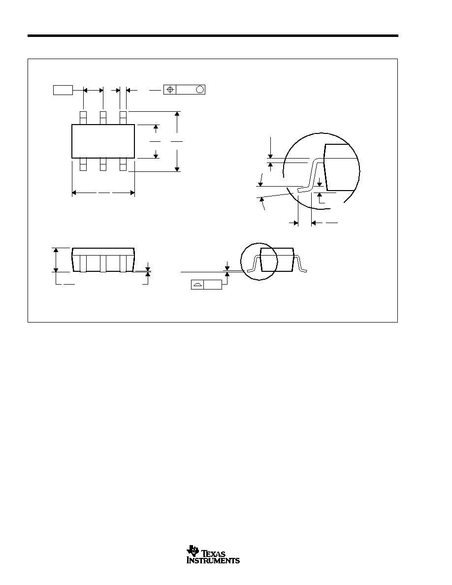
THEORY OF OPERATION
DAC SECTION
The DAC7512 is fabricated using a CMOS process. The
architecture consists of a string DAC followed by an output
buffer amplifier. Since there is no reference input pin, the
power supply (V
DD
) acts as the reference. Figure 1 shows a
block diagram of the DAC architecture.
OUTPUT AMPLIFIER
The output buffer amplifier is capable of generating rail-to-
rail voltages on its output which gives an output range of
0V to V
DD
. It is capable of driving a load of 2k
in parallel
with 1000pF to GND. The source and sink capabilities of the
output amplifier can be seen in the typical characteristics.
The slew rate is 1V/�s with a half-scale settling time of 8�s
with the output unloaded.
FIGURE 1. DAC7512 Architecture.
DAC Register
REF (+)
Resistor
String
REF(�)
Output
Amplifier
GND
V
DD
V
OUT
The input coding to the DAC7512 is straight binary, so the
ideal output voltage is given by:
V
OUT
=
V
DD
�
D
4096
where D = decimal equivalent of the binary code that is
loaded to the DAC register; it can range from 0 to 4095.
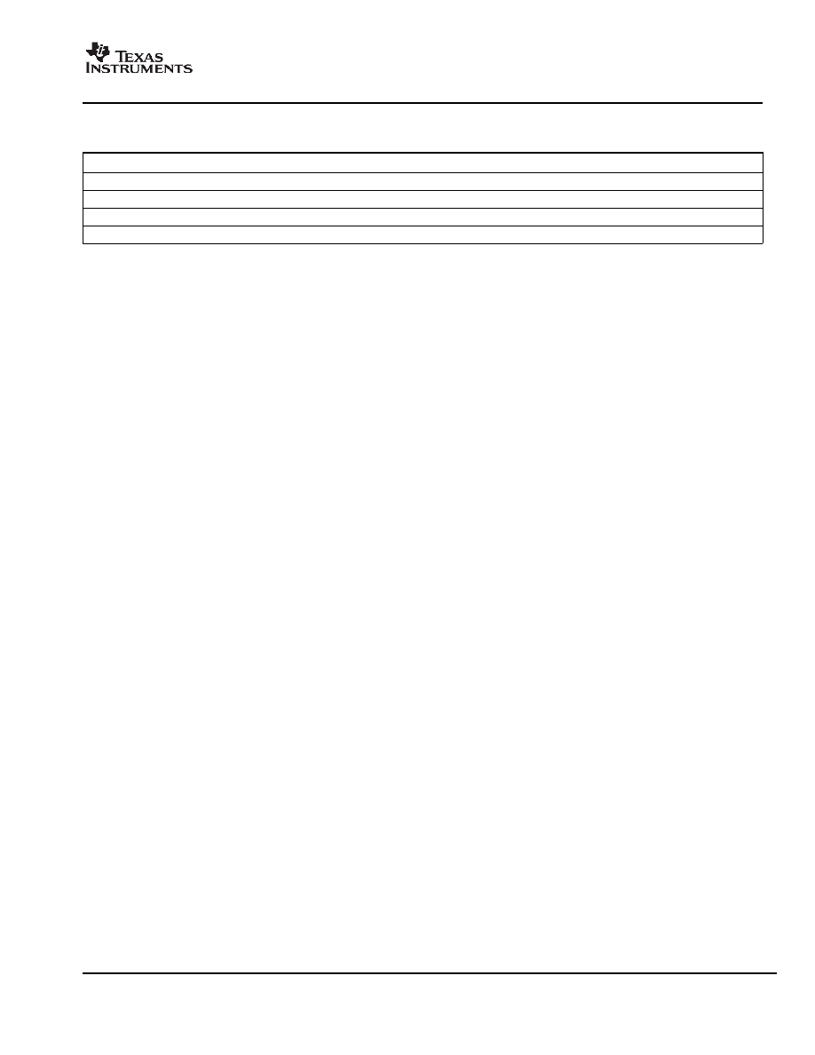
RESISTOR STRING
The resistor string section is shown in Figure 2. It is simply
a string of resistors, each of value R. The code loaded into
the DAC register determines at which node on the string the
voltage is tapped off to be fed into the output amplifier by
closing one of the switches connecting the string to the
amplifier. It is tested monotonic because it is a string of
resistors.
FIGURE 2. Resistor String.
To Output
Amplifier
R
R
R
R
R

DAC7512
12
SBAS156B
www.ti.com
DB13
DB12
OPERATING MODE
0
0
Normal Operation
Power-Down Modes:
0
1
Output 1k
to GND
1
0
Output 100k
to GND
1
1
High-Z
TABLE I. Modes of Operation for the DAC7512.
FIGURE 4. SYNC Interrupt Facility.
CLK
SYNC
D
IN
Invalid Write Sequence:
SYNC HIGH before 16th Falling Edge
Valid Write Sequence: Output Updates
on the 16th Falling Edge
DB15
DB0
DB15
DB0
SERIAL INTERFACE
The DAC7512 has a three-wire serial interface (SYNC,
SCLK, and D
IN
), which is compatible with SPI, QSPI, and
Microwire interface standards as well as most Digital Signal
Processors (DSPs). See the Serial Write Operation timing
diagram for an example of a typical write sequence.
The write sequence begins by bringing the SYNC line LOW.
Data from the D
IN
line is clocked into the 16-bit shift register
on the falling edge of SCLK. The serial clock frequency can
be as high as 30MHz, making the DAC7512 compatible with
high-speed DSPs. On the 16th falling edge of the serial
clock, the last data bit is clocked in and the programmed
function is executed (i.e., a change in DAC register contents
and/or a change in the mode of operation).
At this point, the SYNC line may be kept LOW or brought
HIGH. In either case, it must be brought HIGH for a minimum
of 33ns before the next write sequence so that a falling edge
of SYNC can initiate the next write sequence. Since the
SYNC buffer draws more current when the SYNC signal is
HIGH than it does when it is LOW, SYNC should be idled
LOW between write sequences for lowest power operation of
the part. As mentioned above, however, it must be brought
HIGH again just before the next write sequence.
INPUT SHIFT REGISTER
The input shift register is 16 bits wide, as shown in Figure 3.
The first two bits are "don't cares". The next two bits (PD1
and PD0) are control bits that control which mode of opera-
tion the part is in (normal mode or one of three power-down
modes). There is a more complete description of the various
modes in the Power-Down Modes section. The next 12 bits
are the data bits. These are transferred to the DAC register
on the 16th falling edge of SCLK.
SYNC INTERRUPT
In a normal write sequence, the SYNC line is kept LOW for
at least 16 falling edges of SCLK and the DAC is updated on
the 16th falling edge. However, if SYNC is brought HIGH
before the 16th falling edge, this acts as an interrupt to the
write sequence. The shift register is reset and the write
sequence is seen as invalid. Neither an update of the DAC
register contents or a change in the operating mode occurs,
as shown in Figure 4.
POWER-ON RESET
The DAC7512 contains a power-on reset circuit that controls
the output voltage during power-up. On power-up, the DAC
register is filled with zeros and the output voltage is 0V; it
remains there until a valid write sequence is made to the
DAC. This is useful in applications where it is important to
know the state of the output of the DAC while it is in the
process of powering up.
POWER-DOWN MODES
The DAC7512 contains four separate modes of operation.
These modes are programmable by setting two bits (PD1
and PD0) in the control register. Table I shows how the state
of the bits corresponds to the mode of operation of the
device.
DB15
DB0
X
X
PD1
PD0
D11
D10
D9
D8
D7
D6
D5
D4
D3
D2
D1
D0
FIGURE 3. Data Input Register.
When both bits are set to 0, the part works normally with its
normal power consumption of 135�A at 5V. However, for the
three power-down modes, the supply current falls to 200nA
at 5V (50nA at 3V). Not only does the supply current fall, but
the output stage is also internally switched from the output of
the amplifier to a resistor network of known values. This has
the advantage that the output impedance of the part is known
while the part is in power-down mode. There are three
different options. The output is connected internally to GND
through a 1k
resistor, a 100k
resistor, or it is left open-
circuited (High-Z). See Figure 5 for the output stage.

DAC7512
13
SBAS156B
www.ti.com
FIGURE 5. Output Stage During Power-Down.
Resistor
String DAC
Amplifier
Power-down
Circuitry
Resistor
Network
V
OUT
All linear circuitry is shut down when the power-down mode
is activated. However, the contents of the DAC register are
unaffected when in power-down. The time to exit power-
down is typically 2.5�s for V
DD
= 5V and 5�s for V
DD
= 3V.
See the Typical Characteristics for more information.
MICROPROCESSOR
INTERFACING
DAC7512 TO 8051 INTERFACE
Figure 6 shows a serial interface between the DAC7512 and
a typical 8051-type microcontroller. The setup for the inter-
face is as follows: TXD of the 8051 drives SCLK of the
DAC7512, while RXD drives the serial data line of the part.
The SYNC signal is derived from a bit programmable pin on
the port. In this case, port line P3.3 is used. When data is to
be transmitted to the DAC7512, P3.3 is taken LOW. The
8051 transmits data only in 8-bit bytes; thus only eight falling
clock edges occur in the transmit cycle. To load data to the
DAC, P3.3 is left LOW after the first eight bits are transmitted,
and a second write cycle is initiated to transmit the second
byte of data. P3.3 is taken HIGH following the completion of
this cycle. The 8051 outputs the serial data in a format which
has the LSB first. The DAC7512 requires its data with the
MSB as the first bit received. The 8051 transmit routine must
therefore take this into account, and "mirror" the data as
needed.
FIGURE 6. DAC7512 to 80C51/80L51 Interface.
80C51/80L51
(1)
P3.3
TXD
RXD
DAC7512
(1)
SYNC
SCLK
D
IN
NOTE: (1) Additional pins omitted for clarity.
FIGURE 7. DAC7512 to Microwire Interface.
SYNC
SCLK
D
IN
Microwire
TM
CS
SK
SO
DAC7513
(1)
NOTE: (1) Additional pins omitted for clarity.
Microwire is a registered trademark of National Semiconductor.
DAC7512 TO 68HC11 INTERFACE
Figure 8 shows a serial interface between the DAC7512 and
the 68HC11 microcontroller. SCK of the 68HC11 drives the
SCLK of the DAC7512, while the MOSI output drives the
serial data line of the DAC. The SYNC signal is derived from
a port line (PC7), similar to what was done for the 8051.
FIGURE 8. DAC7512 to 68HC11 Interface.
68HC11
(1)
PC7
SCK
MOSI
SYNC
SCLK
D
IN
DAC7513
(1)
NOTE: (1) Additional pins omitted for clarity.
The 68HC11 should be configured so that its CPOL bit is a
0 and its CPHA bit is a 1. This configuration causes data
appearing on the MOSI output is valid on the falling edge of
SCK. When data is being transmitted to the DAC, the SYNC
line is taken LOW (PC7). Serial data from the 68HC11 is
transmitted in 8-bit bytes with only eight falling clock edges
occurring in the transmit cycle. Data is transmitted MSB first.
In order to load data to the DAC7512, PC7 is left LOW after
the first eight bits are transferred, and a second serial write
operation is performed to the DAC and PC7 is taken HIGH
at the end of this procedure.
APPLICATIONS
USING REF02 AS A POWER
SUPPLY FOR THE DAC7512
Due to the extremely low supply current required by the
DAC7512, an alternative option is to use a REF02 +5V
precision voltage reference to supply the required voltage to
the part, see Figure 9. This is especially useful if the power
supply is too noisy or if the system supply voltages are at
some value other than 5V. The REF02 will output a steady
supply voltage for the DAC7512. If the REF02 is used, the
current it needs to supply to the DAC7512 is 135�A. This is
with no load on the output of the DAC. When the DAC output
DAC7512 TO MICROWIRE
TM
INTERFACE
Figure 7 shows an interface between the DAC7512 and any
Microwire compatible device. Serial data is shifted out on the
falling edge of the serial clock and is clocked into the
DAC7512 on the rising edge of the SK signal.

DAC7512
14
SBAS156B
www.ti.com
FIGURE 10. Bipolar Operation with the DAC7512.
FIGURE 9. REF02 as Power Supply to DAC7512.
REF02
DAC7512
Three-Wire
Serial
Interface
+5V
135
�
A
V
OUT
= 0V to 5V
SYNC
SCLK
D
IN
+15
This is an output voltage range of �5V with 000
H
correspond-
ing to a �5V output and FFF
H
corresponding to a +5V output.
LAYOUT
A precision analog component requires careful layout, ad-
equate bypassing, and clean, well-regulated power supplies.
As the DAC7512 offers single-supply operation, it will often
be used in close proximity with digital logic, microcontrollers,
microprocessors, and digital signal processors. The more
digital logic present in the design and the higher the switch-
ing speed, the more difficult it will be to achieve good
performance from the converter.
Due to the single ground pin of the DAC7512, all return
currents, including digital and analog return currents, must
flow through the GND pin. Ideally, GND would be connected
directly to an analog ground plane. This plane would be
separate from the ground connection for the digital compo-
nents until they were connected at the power entry point of
the system.
The power applied to V
DD
should be well regulated and low
noise. Switching power supplies and DC/DC converters will
often have high-frequency glitches or spikes riding on the
output voltage. In addition, digital components can create
similar high-frequency spikes as their internal logic switches
states. This noise can easily couple into the DAC output
voltage through various paths between the power connec-
tions and analog output. This is particularly true for the
DAC7512, as the power supply is also the reference voltage
for the DAC.
As with the GND connection, V
DD
should be connected to a
+5V power supply plane or trace that is separate from the
connection for digital logic until they are connected at the
power entry point. In addition, the 1�F to 10�F and 0.1�F
bypass capacitors are strongly recommended. In some situ-
ations, additional bypassing may be required, such as a
100�F electrolytic capacitor or even a "Pi" filter made up of
inductors and capacitors--all designed to essentially low-
pass filter the +5V supply, removing the high-frequency noise.
is loaded, the REF02 also needs to supply the current to the
load. The total current required (with a 5k
load on the DAC
output) is:
135�A + (5V/5k
) = 1.14mA
The load regulation of the REF02 is typically 0.005%/mA,
which results in an error of 285�V for the 1.14mA current
drawn from it. This corresponds to a 0.2LSB error.
BIPOLAR OPERATION USING THE DAC7512
The DAC7512 has been designed for single-supply operation
but a bipolar output range is also possible using the circuit in
Figure 10. The circuit shown will give an output voltage range
of �5V. Rail-to-rail operation at the amplifier output is achiev-
able using an OPA340 as the output amplifier.
The output voltage for any input code can be calculated as
follows:
V
O
=
V
�
D
4096
�
R
1
+
R
2
R
1
� V
DD
�
R
2
R
1
where D represents the input code in decimal (0 - 4095).
With V
DD
= 5V, R
1
= R
2
= 10k
:
V
O
=
10
�
D
4096
� 5V
DAC7512
V
DD
V
OUT
R
1
10k
R
2
10k
Three-Wire
Serial
Interface
5V
10 F
0.1 F
--5V
�5V
+5V
OPA703
DAC7512
15
SBAS156B
www.ti.com
PACKAGE DRAWINGS
MPDS028B � JUNE 1997 � REVISED SEPTEMBER 2001
DGK (R-PDSO-G8)
PLASTIC SMALL-OUTLINE PACKAGE
0,69
0,41
0,25
0,15 NOM
Gage Plane
4073329/C 08/01
4,98
0,25
5
3,05
4,78
2,95
8
4
3,05
2,95
1
0,38
1,07 MAX
Seating Plane
0,65
M
0,08
0
�
� 6
�
0,10
0,15
0,05
NOTES: A. All linear dimensions are in millimeters.
B. This drawing is subject to change without notice.
C. Body dimensions do not include mold flash or protrusion.
D. Falls within JEDEC MO-187
DAC7512
16
SBAS156B
www.ti.com
PACKAGE DRAWINGS
(Cont.)
MPDS026D FEBRUARY 1997 REVISED FEBRUARY 2002
DBV (R-PDSO-G6)
PLASTIC SMALL-OUTLINE
0,10
M
0,20
0,95
0
�
8
�
0,25
0,55
0,35
Gage Plane
0,15 NOM
4073253-5/G 01/02
2,60
3,00
0,50
0,25
1,50
1,70
4
6
3
1
2,80
3,00
1,45
0,95
0,05 MIN
Seating Plane
6X
NOTES: A. All linear dimensions are in millimeters.
B. This drawing is subject to change without notice.
C. Body dimensions do not include mold flash or protrusion.
D. Leads 1, 2, 3 may be wider than leads 4, 5, 6 for package orientation.
PACKAGING INFORMATION
ORDERABLE DEVICE
STATUS(1)
PACKAGE TYPE
PACKAGE DRAWING
PINS
PACKAGE QTY
DAC7512E/250
ACTIVE
VSSOP
DGK
8
250
DAC7512E/2K5
ACTIVE
VSSOP
DGK
8
2500
DAC7512N/250
ACTIVE
SOP
DBV
6
250
DAC7512N/3K
ACTIVE
SOP
DBV
6
1
(1) The marketing status values are defined as follows:
ACTIVE: Product device recommended for new designs.
LIFEBUY: TI has announced that the device will be discontinued, and a lifetime-buy period is in effect.
NRND: Not recommended for new designs. Device is in production to support existing customers, but TI does not recommend using this part in
a new design.
PREVIEW: Device has been announced but is not in production. Samples may or may not be available.
OBSOLETE: TI has discontinued the production of the device.
PACKAGE OPTION ADDENDUM
www.ti.com
13-Oct-2003

IMPORTANT NOTICE
Texas Instruments Incorporated and its subsidiaries (TI) reserve the right to make corrections, modifications,
enhancements, improvements, and other changes to its products and services at any time and to discontinue
any product or service without notice. Customers should obtain the latest relevant information before placing
orders and should verify that such information is current and complete. All products are sold subject to TI's terms
and conditions of sale supplied at the time of order acknowledgment.
TI warrants performance of its hardware products to the specifications applicable at the time of sale in
accordance with TI's standard warranty. Testing and other quality control techniques are used to the extent TI
deems necessary to support this warranty. Except where mandated by government requirements, testing of all
parameters of each product is not necessarily performed.
TI assumes no liability for applications assistance or customer product design. Customers are responsible for
their products and applications using TI components. To minimize the risks associated with customer products
and applications, customers should provide adequate design and operating safeguards.
TI does not warrant or represent that any license, either express or implied, is granted under any TI patent right,
copyright, mask work right, or other TI intellectual property right relating to any combination, machine, or process
in which TI products or services are used. Information published by TI regarding third-party products or services
does not constitute a license from TI to use such products or services or a warranty or endorsement thereof.
Use of such information may require a license from a third party under the patents or other intellectual property
of the third party, or a license from TI under the patents or other intellectual property of TI.
Reproduction of information in TI data books or data sheets is permissible only if reproduction is without
alteration and is accompanied by all associated warranties, conditions, limitations, and notices. Reproduction
of this information with alteration is an unfair and deceptive business practice. TI is not responsible or liable for
such altered documentation.
Resale of TI products or services with statements different from or beyond the parameters stated by TI for that
product or service voids all express and any implied warranties for the associated TI product or service and
is an unfair and deceptive business practice. TI is not responsible or liable for any such statements.
Following are URLs where you can obtain information on other Texas Instruments products and application
solutions:
Products
Applications
Amplifiers
amplifier.ti.com
Audio
www.ti.com/audio
Data Converters
dataconverter.ti.com
Automotive
www.ti.com/automotive
DSP
dsp.ti.com
Broadband
www.ti.com/broadband
Interface
interface.ti.com
Digital Control
www.ti.com/digitalcontrol
Logic
logic.ti.com
Military
www.ti.com/military
Power Mgmt
power.ti.com
Optical Networking
www.ti.com/opticalnetwork
Microcontrollers
microcontroller.ti.com
Security
www.ti.com/security
Telephony
www.ti.com/telephony
Video & Imaging
www.ti.com/video
Wireless
www.ti.com/wireless
Mailing Address:
Texas Instruments
Post Office Box 655303 Dallas, Texas 75265
Copyright
2003, Texas Instruments Incorporated