
Low Cost 12-Bit CMOS
Four-Quadrant Multiplying
DIGITAL-TO-ANALOG CONVERTER
FEATURES
q
FULL FOUR-QUADRANT
MULTIPLICATION
q
12-BIT END-POINT LINEARITY
q
DIFFERENTIAL LINEARITY
±
1/2LSB MAX
OVER TEMPERATURE
q
MONOTONICITY GUARANTEED OVER
TEMPERATURE
q
TTL-/CMOS-COMPATIBLE
q
SINGLE +5V TO +15V SUPPLY
q
LATCH-UP RESISTANT
q
7521/7541/7541A REPLACEMENT
q
PACKAGES: Plastic DIP, Plastic SOIC
q
LOW COST
DESCRIPTION
The Burr-Brown DAC7541A is a low cost 12-bit,
four-quadrant multiplying digital-to-analog converter.
Laser-trimmed thin-film resistors on a monolithic
CMOS circuit provide true 12-bit integral and differ-
ential linearity over the full specified temperature
range.
DAC7541A is a direct, improved pin-for-pin replace-
ment for 7521, 7541, and 7541A industry standard
parts. In addition to a standard 18-pin plastic package,
the DAC7541A is also available in a surface-mount
plastic 18-pin SOIC.
10k
10k
20k
20k
10k
20k
10k
20k
10k
20k
I
OUT 2
Bit 11
Bit 3
Bit 2
Bit 1
(MSB)
V
REF
Bit 12
(LSB)
20k
I
OUT 1
R
FB
SPDT NMOS
Switches
Digital Inputs (DTL-/TTL-/CMOS-compatible)
Logic: A switch is closed to I
OUT 1
for its digital input in a "HIGH" state.
Switches shown for digital inputs "HIGH".
DAC7541A
Æ
International Airport Industrial Park ∑ Mailing Address: PO Box 11400 ∑ Tucson, AZ 85734 ∑ Street Address: 6730 S. Tucson Blvd. ∑ Tucson, AZ 85706
Tel: (520) 746-1111 ∑ Twx: 910-952-1111 ∑ Cable: BBRCORP ∑ Telex: 066-6491 ∑ FAX: (520) 889-1510 ∑ Immediate Product Info: (800) 548-6132
©
1987 Burr-Brown Corporation
PDS-639C
Printed in U.S.A. September, 1993
SBAS147
2
Æ
DAC7541A
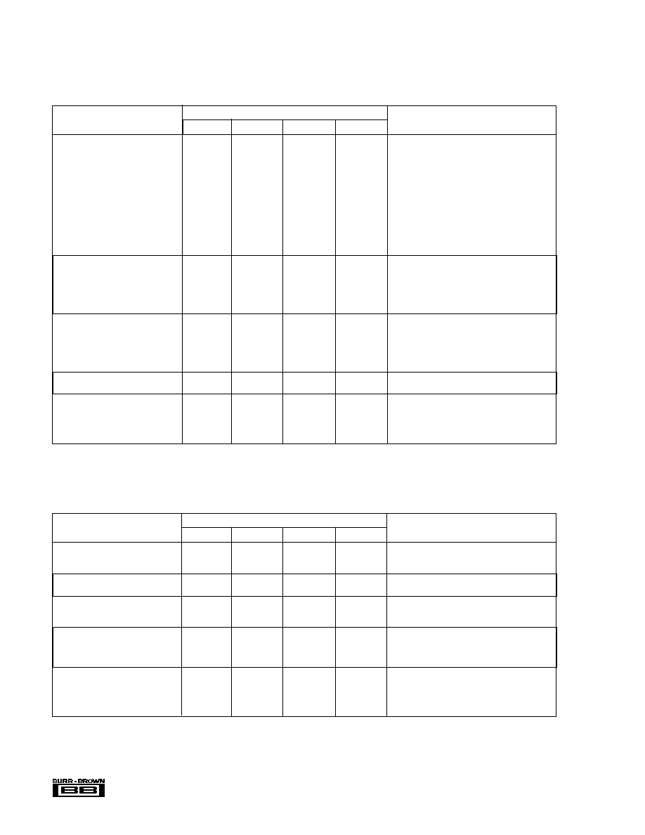
PARAMETER
GRADE
T
A
= +25
∞
C
T
A
= T
MAX
, T
MIN
(1)
UNITS
TEST CONDITIONS/COMMENTS
PROPAGATION DELAY
(from Digital Input change to 90% of
Out
1
Load = 100
, C
EXT
= 13pF.
final Analog Output)
All
100
--
ns typ
Digital Inputs = 0V to V
DD
or V
DD
to 0V.
DIGITAL-TO-ANALOG GLITCH
V
REF
= 0V, all digital inputs 0V to V
DD
or V
DD
to
IMPULSE
All
1000
--
nV-s typ
0V. Measured using OPA606 as output amplifier.
MULTIPLYING FEEDTHROUGH
ERROR
(V
REF
to Out
1
)
All
1.0
--
mVp-p max
V
REF
=
±
10V, 10kHz sine wave.
OUTPUT CURRENT SETTLING TIME
All
0.6
--
µ
s typ
To 0.01% of Full Scale Range.
Out
1
Load = 100
, C
EXT
= 13pF.
All
1.0
--
µ
s max
Digital Inputs: 0V to V
DD
or V
DD
to 0V.
OUTPUT CAPACITANCE
C
OUT 1
(Pin 1)
All
100
100
pF max
Digital Inputs = V
IH
C
OUT 2
(Pin 2)
All
60
60
pF max
Digital Inputs = V
IH
C
OUT 1
(Pin 1)
All
70
70
pF max
Digital Inputs = V
IL
C
OUT 2
(Pin 2)
All
100
100
pF max
Digital Inputs = V
IL
PARAMETER
GRADE
T
A
= +25
∞
C
T
A
= T
MAX
, T
MIN
(1)
UNITS
TEST CONDITIONS/COMMENTS
ACCURACY
Resolution
All
12
12
Bits
Relative Accuracy
J
±
1
±
1
LSB max
±
1LSB =
±
0.024% of FSR.
K
±
1/2
±
1/2
LSB max
±
1/2LSB =
±
0.012% of FSR.
Differential Non-linearity
J
±
1
±
1
LSB max
All grades guaranteed monotonic to 12 bits,
K
±
1/2
±
1/2
LSB max
T
MIN
to T
MAX
.
Gain Error
J
±
6
±
8
LSB max
Measured using internal R
FB
and includes effect
K
±
1
±
3
LSB max
of leakage current and gain T.C.
Gain error can be trimmed to zero.
Gain Temperature Coefficient
(
Gain/
Temperature)
ALL
5
ppm/
∞
C max
Typical value is 2ppm/
∞
C.
Output Leakage Current: Out
1
(Pin 1)
J, K
±
5
±
10
nA max
All digital inputs = 0V.
Out
2
(Pin 2)
J, K
±
5
±
10
nA max
All digital inputs = V
DD
.
REFERENCE INPUT
Voltage (Pin 17 to GND)
All
≠10/+10
≠10/+10
V min/max
Input Resistance (Pin 17 to GND)
All
7-18
7-18
k
min/max
Typical input resistance = 11k
.
Typical input resistance temperature coefficient is
≠50ppm/
∞
C.
DIGITAL INPUTS
V
IN
(Input HIGH Voltage)
All
2.4
2.4
V min
V
IL
(Input LOW Voltage)
All
0.8
0.8
V max
I
IN
(Input Current)
All
±
1
±
1
µ
A max
Logic inputs are MOS gates.
I
IN
typ (25
∞
C) = 1nA
C
IN
(Input Capacitance)
(2)
All
8
8
pF max
V
IN
= 0V
POWER SUPPLY REJECTION
Gain/
V
DD
All
±
0.01
±
0.02
% per % max
V
DD
= +11.4V to +16V
POWER SUPPLY
V
DD
Range
All
+5 to +16
+5 to +16
V min to
Accuracy is not guaranteed over this range.
V max
I
DD
All
2
2
mA max
All digital inputs V
IL
or V
IN
.
All
100
500
µ
A max
All digital inputs 0V or V
DD
.
SPECIFICATIONS
ELECTRICAL
At +25
∞
C, +V
DD
= +12V or +15V, V
REF
= +10V, V
PIN 1
= V
PIN 2
= 0V, unless otherwise specified.
NOTES: (1) Temperature ranges are: = 0
∞
C to + 70
∞
C for JP, KP, JU and KU versions. (2) Guaranteed by design but not production tested.
DAC7541A
AC PERFORMANCE CHARACTERISTICS
These characteristics are included for design guidance only and are not production tested.
V
DD
= +15V, V
REF
= +10V except where stated, V
PIN 1
= V
PIN 2
= 0V, output amp is OPA606 except where stated.
DAC7541A
NOTE: (1) Temperature ranges are: = 0
∞
C to + 70
∞
C for JP, KP, JU and KU versions.

3
Æ
DAC7541A
TEMPERATURE
RELATIVE
MODEL
PACKAGE
RANGE
ACCURACY (LSB)
GAIN ERROR (LSB)
DAC7541AJP
Plastic DIP
0
∞
C to +70
∞
C
±
1
±
6
DAC7541AKP
Plastic DIP
0
∞
C to +70
∞
C
±
1/2
±
1
DAC7541AJU
Plastic SOIC
0
∞
C to +70
∞
C
±
1
±
6
DAC7541AKU
Plastic SOIC
0
∞
C to +70
∞
C
±
1/2
±
1
BURN-IN SCREENING OPTION
See text for details.
ABSOLUTE MAXIMUM RATINGS
(1)
PIN CONNECTIONS
V
DD
(Pin 16) to Ground ...................................................................... +17V
V
REF
(Pin 17) to Ground ..................................................................... +25V
V
RPB
(Pin 18) to Ground .....................................................................
±
25V
Digital Input Voltage (pins 4-15) to Ground ............................... ≠0.4V, V
DD
V
PIN 1
, V
PIN 2
to Ground ............................................................. ≠0.4V, V
DD
Power Dissipation (any Package):
To +75
∞
C ..................................................................................... 450mW
Derates above +75
∞
C .............................................................. ≠6mW/
∞
C
Lead Temperature (soldering, 10s) ................................................ +300
∞
C
Storage Temperature: Plastic Package ......................................... +125
∞
C
NOTE: (1) Stresses above those listed above may cause permanent damage to
the device. This is a stress rating only and functional operation of the device at
these or any other condition above those indicated in the operational sections of
this specification is not implied. Exposure to absolute maximum rating conditions
for extended periods may affect device reliability.
The information provided herein is believed to be reliable; however, BURR-BROWN assumes no responsibility for inaccuracies or omissions. BURR-BROWN
assumes no responsibility for the use of this information, and all use of such information shall be entirely at the user's own risk. Prices and specifications are subject
to change without notice. No patent rights or licenses to any of the circuits described herein are implied or granted to any third party. BURR-BROWN does not
authorize or warrant any BURR-BROWN product for use in life support devices and/or systems.
Top View
DIP/SOIC
ELECTROSTATIC
DISCHARGE SENSITIVITY
The DAC7541A is an ESD (electrostatic discharge) sensi-
tive device. The digital control inputs have a special FET
structure, which turns on when the input exceeds the supply
by 18V, to minimize ESD damage. However, permanent
damage may occur on unconnected devices subject to high
energy electrostatic fields. When not in use, devices must be
stored in conductive foam or shunts. The protective foam
should be discharged to the destination socket before
devices are removed.
BURN-IN SCREENING
Burn-in screening is an option available for the models in the
Ordering Information table. Burn-in duration is 160 hours at
the indicated temperature (or equivalent combination of time
and temperature).
All units are tested after burn-in to ensure that grade speci-
fications are met. To order burn-in, add "-BI" to the base
model number.
PACKAGE INFORMATION
PACKAGE DRAWING
MODEL
PACKAGE
NUMBER
(1)
DAC7541JP
Plastic DIP
218
DAC7541KP
Plastic DIP
218
DAC7541JU
Plastic SOIC
219
DAC7541KU
Plastic SOIC
219
DAC7541JP-BI
Plastic DIP
218
DAC7541KP-BI
Plastic DIP
218
NOTE: (1) For detailed drawing and dimension table, please see end of data
sheet, or Appendix D of Burr-Brown IC Data Book.
DAC7541A
1
2
3
4
5
6
7
8
9
18
17
16
15
14
13
12
11
10
I
OUT 1
I
OUT 2
GND
Bit 1 (MSB)
Bit 2
Bit 3
Bit 4
Bit 5
Bit 6
R
FB
V
REF
+V
DD
Bit 12
(LSB)
Bit 11
Bit 10
Bit 9
Bit 8
Bit 7
TEMPERATURE
RELATIVE
BURN-IN TEMP.
MODEL
PACKAGE
RANGE
ACCURACY (LSB)
(160 Hours)
(1)
DAC7541AJP-BI
Plastic DIP
0
∞
C to +70
∞
C
±
1
+85
∞
C
DAC7541AKP-BI
Plastic DIP
0
∞
C to +70
∞
C
±
1/2
+85
∞
C
ORDERING INFORMATION

4
Æ
DAC7541A
TYPICAL PERFORMANCE CURVES
T
A
= +25
∞
C, V
DD
= +15V, unless otherwise noted.
MECHANICAL INFORMATION
MILS (0.001")
MILLIMETERS
Die Size
104 x 105
±
5
2.64 x 2.67
±
0.13
Die Thickness
20
±
3
0.51
±
0.08
Min. Pad Size
4 x 4
0.10 x 0.10
Metalization
Aluminum
PAD
FUNCTION
1
I
OUT1
2
I
OUT2
3
GND
4
Bit 1 (MSB)
5
Bit 2
6
Bit 3
7
Bit 4
8
Bit 5
9
Bit 6
PAD
FUNCTION
10
Bit 7
11
Bit 8
12
Bit 9
13
Bit 10
14
Bit 11
15
Bit 12 (LSB)
16
+V
DD
17
V
REF
18
R
FEEDBACK
Substrate Bias: Isolated.
NC: No Connection.
DIE TOPOLOGY DAC7541A
0
GAIN ERROR vs SUPPLY VOLTAGE
Gain Error (LSB)
0
15
3
5/2
2
3/2
1
1/2
Supply Voltage (V)
5
10
0.001
Frequency (Hz)
FEEDTHROUGH ERROR vs FREQUENCY
Feedthrough (% FSR)
1M
1k
10k
100
100k
10
1
0.10
0.010
0
LINEARITY vs SUPPLY VOLTAGE
Linearity Error (LSB)
0
15
3/2
5/4
1
3/4
1/2
1/4
Supply Voltage (V)
5
10
0
SUPPLY CURRENT vs SUPPLY VOLTAGE
Supply Current (µA)
0
15
3/2
5/4
1
3/4
1/2
1/4
Supply Voltage (V)
5
10
V
IH
= +2.4V
V
IH
= V
DD

5
Æ
DAC7541A
DISCUSSION
OF SPECIFICATIONS
RELATIVE ACCURACY
This term (also known as linearity) describes the transfer
function of analog output to digital input code. The linearity
error describes the deviation from a straight line between
zero and full scale.
DIFFERENTIAL NONLINEARITY
Differential nonlinearity is the deviation from an ideal 1LSB
change in the output, from one adjacent output state to the
next. A differential nonlinearity specification of
±
1.0LSB
guarantees monotonicity.
GAIN ERROR
Gain error is the difference in measure of full-scale output
versus the ideal DAC output. The ideal output for the
DAC7541A is ≠(4095/4096)
X
(V
REF
). Gain error may be
adjusted to zero using external trims.
OUTPUT LEAKAGE CURRENT
The measure of current which appears at Out
1
with the DAC
loaded with all zeros, or at Out
2
with the DAC loaded with
all ones.
MULTIPLYING FEEDTHROUGH ERROR
This is the AC error output due to capacitive feedthrough
from V
REF
to Out
1
with the DAC loaded with all zeros. This
test is performed at 10kHz.
OUTPUT CURRENT SETTLING TIME
This is the time required for the output to settle to a tolerance
of
±
0.5LSB of final value from a change in code of all zeros
to all ones, or all ones to all zeros.
PROPAGATION DELAY
This is the measure of the delay of the internal circuitry and
is measured as the time from a digital code change to the
point at which the output reaches 90% of final value.
DIGITAL-TO-ANALOG GLITCH IMPULSE
This is the measure of the area of the glitch energy measured
in nV-seconds. Key contributions to glitch energy are digital
word-bit timing differences, internal circuitry timing differ-
ences, and charge injected from digital logic.
MONOTONICITY
Monotonicity assures that the analog output will increase or
stay the same for increasing digital input codes. The
DAC7541A is guaranteed monotonic to 12 bits.
POWER SUPPLY REJECTION
Power supply rejection is the measure of the sensitivity of
the output (full scale) to a change in the power supply
voltage.
FIGURE 1. Simplified DAC Circuit.
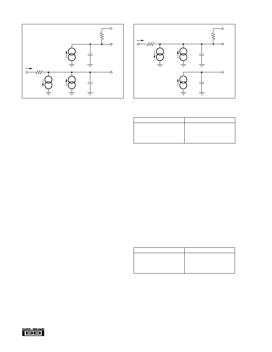
EQUIVALENT CIRCUIT ANALYSIS
Figures 2 and 3 show the equivalent circuits for all digital
inputs low and high, respectively. The reference current is
switched to I
OUT 2
when all inputs are low and I
OUT 1
when
inputs are high. The I
L
current source is the combination of
surface and junction leakages to the substrate; the
1/4096 current source represents the constant one-bit current
drain through the ladder terminal.
DYNAMIC PERFORMANCE
Output Impedance
The output resistance, as in the case of the output capaci-
tance, is also modulated by the digital input code. The
resistance looking back into the I
OUT 1
terminal may be
anywhere between 10k
(the feedback resistor alone when
all digital inputs are low) and 7.5k
(the feedback resistor
in parallel with approximately 30k
of the R-2R ladder
network resistance when any single bit logic is high). The
static accuracy and dynamic performance will be affected by
this modulation. The gain and phase stability of the output
CIRCUIT DESCRIPTION
The DAC7541A is a 12-bit multiplying D/A converter
consisting of a highly stable thin-film R-2R ladder network
and 12 pairs of current steering switches on a monolithic
chip. Most applications require the addition of a voltage or
current reference and an output operational amplifier.
A simplified circuit of the DAC7541A is shown in Figure 1.
The R-2R inverted ladder binarily divides the input currents
that are switched between I
OUT 1
and I
OUT 2
bus lines. This
switching allows a constant current to be maintained in each
ladder leg independent of the input code.
The input resistance at V
REF
(Figure 1) is always equal to
R
LDR
(R
LDR
is the R/2R ladder characteristic resistance and
is equal to value "R"). Since R
IN
at the V
REF
pin is constant,
the reference terminal can be driven by a reference voltage
or a reference current, AC or DC, of positive or negative
polarity.
Bit 12
(LSB)
10k
10k
20k
20k
10k
20k
20k
I
OUT 2
Bit 3
Bit 2
Bit 1
(MSB)
V
REF
20k
I
OUT 1
R
FB
Digital Inputs (DTL-/TTL-/CMOS-compatible)
Switches shown for digital inputs "HIGH".
S
2
S
1
S
3
S
12
6
Æ
DAC7541A
FIGURE 2. DAC7541A Equivalent Circuit (All inputs
LOW).
FIGURE 3. DAC7541A Equivalent Circuit (All inputs
HIGH).
1/4096
I
L
90pF
I
L
60pF
R = 10k
R
FB
I
OUT 1
I
OUT 2
I
REF
V
REF
R
10k
1/4096
I
L
90pF
I
L
55pF
R = 10k
R
FB
I
OUT 2
I
OUT 1
R
10k
I
REF
V
REF
amplifier, board layout, and power supply decoupling will
all affect the dynamic performance of the DAC7541A. The
use of a compensation capacitor may be required when high-
speed operational amplifiers are used. It may be connected
across the amplifier's feedback resistor to provide the nec-
essary phase compensation to critically dampen the output.
See Figures 4 and 6.
APPLICATIONS
OP AMP CONSIDERATIONS
The input bias current of the op amp flows through the
feedback resistor, creating an error voltage at the output of
the op amp. This will show up as an offset through all codes
of the transfer characteristics. A low bias current op amp
such as the OPA606 is recommended.
Low offset voltage and V
OS
drift are also important. The
output impedance of the DAC is modulated with the digital
code. This impedance change (approximately 10k
to 30k
)
is a change in closed-loop gain to the op amp. The result is
that V
OS
will be multiplied by a factor of one to two
depending on the code. This shows up as a linearity error.
Offset can be adjusted out using Figure 4. Gain may be
adjusted using Figure 5.
UNIPOLAR BINARY OPERATION
(Two-Quadrant Multiplication)
Figure 4 shows the analog circuit connections required for
unipolar binary (two-quadrant multiplication) operation. With
a DC reference voltage or current (positive or negative
polarity) applied at pin 17, the circuit is a unipolar D/A
converter. With an AC reference voltage or current, the
circuit provides two-quadrant multiplication (digitally con-
trolled attenuation). The input/output relationship is shown
in Table I.
BINARY INPUT
ANALOG OUTPUT
MSB
LSB
1111 1111 1111
≠V
REF
(4095/4096)
1000 0000 0000
≠V
REF
(2048/4096)
0000 0000 0001
≠V
REF
(1/4096)
0000 0000 0000
0V
TABLE I. Unipolar Codes.
C
1
phase compensation (10 to 25pF) in Figure 4 may be
required for stability when using high speed amplifiers. C
1
is used to cancel the pole formed by the DAC internal
feedback resistance and output capacitance at Out
1
.
R
1
in Figure 5 provides full scale trim capability--load the
DAC register to 1111 1111 1111, adjust R
1
for V
OUT
= ≠
V
REF
(4095/4096). Alternatively, full scale can be adjusted
by omitting R
1
and R
2
and trimming the reference voltage
magnitude.
BIPOLAR FOUR-QUADRANT OPERATION
Figure 6 shows the connections for bipolar four-quadrant
operation. Offset can be adjusted with the A
1
to A
2
summing
resistor, with the input code set to 1000 0000 0000. Gain
may be adjusted by varying the feedback resistor of A
2
. The
input/output relationship is shown in Table II.
BINARY INPUT
ANALOG OUTPUT
MSB
LSB
1111 1111 1111
+V
REF
(2047/2048)
1000 0000 0000
0V
0111 1111 1111
≠V
REF
(1/2048)
0000 0000 0000
≠V
REF
(2048/2048)
TABLE II. Bipolar Codes.

7
Æ
DAC7541A
FIGURE 4. Basic Connection With Op Amp V
OS
Adjust: Unipolar (two-quadrant) Multiplying Configuration.
FIGURE 5. Basic Connection With Gain Adjust (allows adjustment up or down).
FIGURE 6. Bipolar Four-Quadrant Multiplier.
16
R
F
DAC7541A
Out
1
C
1
B
1
V
REF
V
OUT
2
1
4
∑
5
∑
6
∑
7
∑
8
∑
9
∑
10
∑
11
∑
12
∑
13
∑
14
B
12
15
3
18
OPA604
17
+15V
Out
2
10k
+V
CC
V
OUT
= ≠V
REF
+ + + ∑ ∑ ∑ +
B
1
2
(
B
2
4
B
3
8
B
12
4096
)
≠10V
V
REF
+10V
4095
4096
0
V
OUT
≠ V
REF
Where: B
N
= 1 if the B
N
digital input is HIGH.
B
N
= 0 if the B
N
digital input is LOW.
MSB
Single-Point Ground
16
DAC7541A
B
1
V
REF
2
1
4
∑
5
∑
6
∑
7
∑
8
∑
9
∑
10
∑
11
∑
12
∑
13
∑
14
B
12
15
3
18
OPA604
17
+15V
10k
+V
CC
MSB
R
1
200
R
2
200k
OPA604
or
1/2 OPA2604
V
REF
47
DAC7541A
Bits 1-12
C
1
33pF
+V
DD
4...15
V
OUT
10k
20k
20k
2
1
16
18
17
OPA604
or
1/2 OPA2604
3
5k
V
OUT
= +V
REF
+ + + ∑ ∑ ∑ + ≠ 1
B
1
1
(
B
2
2
B
3
4
B
12
2048
)
A
1
A
2

8
Æ
DAC7541A
DIGITALLY CONTROLLED GAIN BLOCK
The DAC7541A may be used in a digitally controlled gain
block as shown in Figure 7. This circuit gives a range of gain
from one (all bits = one) to 4096 (LSB = one). The transfer
function is:
All bits off is an illegal state, as division by zero is impos-
sible (no op amp feedback). Also, errors increase as gain
increases, and errors are minimized at major carries (only
one bit on at a time).
V
OUT
=
+ + + ∑ ∑ ∑ +
B
1
2
B
3
8
B
2
4
B
12
4096
≠V
IN
(
)
FIGURE 7. Digitally Programmable Gain Block.
Bits 1 to 12
V
OUT
OPA604
DAC7541A
2
3
1
18
17
16
V
DD
V
IN

PACKAGING INFORMATION
ORDERABLE DEVICE
STATUS(1)
PACKAGE TYPE
PACKAGE DRAWING
PINS
PACKAGE QTY
DAC7541AJP
ACTIVE
PDIP
N
18
20
DAC7541AJU
ACTIVE
SOP
DTC
18
43
DAC7541AKP
ACTIVE
PDIP
N
18
20
DAC7541AKU
ACTIVE
SOP
DTC
18
43
DAC7541AKU/1K
ACTIVE
SOP
DTC
18
1000
(1) The marketing status values are defined as follows:
ACTIVE: Product device recommended for new designs.
LIFEBUY: TI has announced that the device will be discontinued, and a lifetime-buy period is in effect.
NRND: Not recommended for new designs. Device is in production to support existing customers, but TI does not recommend using this part in
a new design.
PREVIEW: Device has been announced but is not in production. Samples may or may not be available.
OBSOLETE: TI has discontinued the production of the device.
PACKAGE OPTION ADDENDUM
www.ti.com
3-Oct-2003

IMPORTANT NOTICE
Texas Instruments Incorporated and its subsidiaries (TI) reserve the right to make corrections, modifications,
enhancements, improvements, and other changes to its products and services at any time and to discontinue
any product or service without notice. Customers should obtain the latest relevant information before placing
orders and should verify that such information is current and complete. All products are sold subject to TI's terms
and conditions of sale supplied at the time of order acknowledgment.
TI warrants performance of its hardware products to the specifications applicable at the time of sale in
accordance with TI's standard warranty. Testing and other quality control techniques are used to the extent TI
deems necessary to support this warranty. Except where mandated by government requirements, testing of all
parameters of each product is not necessarily performed.
TI assumes no liability for applications assistance or customer product design. Customers are responsible for
their products and applications using TI components. To minimize the risks associated with customer products
and applications, customers should provide adequate design and operating safeguards.
TI does not warrant or represent that any license, either express or implied, is granted under any TI patent right,
copyright, mask work right, or other TI intellectual property right relating to any combination, machine, or process
in which TI products or services are used. Information published by TI regarding third-party products or services
does not constitute a license from TI to use such products or services or a warranty or endorsement thereof.
Use of such information may require a license from a third party under the patents or other intellectual property
of the third party, or a license from TI under the patents or other intellectual property of TI.
Reproduction of information in TI data books or data sheets is permissible only if reproduction is without
alteration and is accompanied by all associated warranties, conditions, limitations, and notices. Reproduction
of this information with alteration is an unfair and deceptive business practice. TI is not responsible or liable for
such altered documentation.
Resale of TI products or services with statements different from or beyond the parameters stated by TI for that
product or service voids all express and any implied warranties for the associated TI product or service and
is an unfair and deceptive business practice. TI is not responsible or liable for any such statements.
Following are URLs where you can obtain information on other Texas Instruments products and application
solutions:
Products
Applications
Amplifiers
amplifier.ti.com
Audio
www.ti.com/audio
Data Converters
dataconverter.ti.com
Automotive
www.ti.com/automotive
DSP
dsp.ti.com
Broadband
www.ti.com/broadband
Interface
interface.ti.com
Digital Control
www.ti.com/digitalcontrol
Logic
logic.ti.com
Military
www.ti.com/military
Power Mgmt
power.ti.com
Optical Networking
www.ti.com/opticalnetwork
Microcontrollers
microcontroller.ti.com
Security
www.ti.com/security
Telephony
www.ti.com/telephony
Video & Imaging
www.ti.com/video
Wireless
www.ti.com/wireless
Mailing Address:
Texas Instruments
Post Office Box 655303 Dallas, Texas 75265
Copyright
2003, Texas Instruments Incorporated