 | –≠–ª–µ–∫—Ç—Ä–æ–Ω–Ω—ã–π –∫–æ–º–ø–æ–Ω–µ–Ω—Ç: DAC7545LP | –°–∫–∞—á–∞—Ç—å:  PDF PDF  ZIP ZIP |

CMOS 12-Bit Multiplying
DIGITAL-TO-ANALOG CONVERTER
Microprocessor Compatible
FEATURES
q
FOUR-QUADRANT MULTIPLICATION
q
LOW-GAIN TC: 2ppm/
∞
C typ
q
MONOTONICITY ENSURED OVER TEMPERATURE
q
SINGLE 5V TO 15V SUPPLY
q
TTL/CMOS LOGIC COMPATIBLE
q
LOW OUTPUT LEAKAGE: 10nA max
q
LOW OUTPUT CAPACITANCE: 70pF max
q
DIRECT REPLACEMENT FOR THE AD7545,
PM-7545
DESCRIPTION
The DAC7545 is a low-cost, CMOS, 12-bit, four-quadrant
multiplying, digital-to-analog converter (DAC) with input data
latches. The input data is loaded into the DAC as a 12-bit
data word. The data flows through to the DAC when both the
chip select (CS ) and the write (WR) pins are at a logic low.
Laser-trimmed thin-film resistors and excellent CMOS volt-
age switches provide true 12-bit integral and differential
linearity. The device operates on a single +5V to +15V supply
and is available in an SO-20 package; devices are specified
over the commercial temperature range.
The DAC7545 is well suited for battery-powered or other low-
power applications because the power dissipation is less than
0.5mW when used with CMOS logic inputs and V
DD
= +5V.
12-Bit
Multiplying DAC
AGND
OUT 1
DB
11
-DB
0
(Pins 4-15)
WR
CS
17
Input
Data Latches
12
12
16
19
V
REF
20
R
FB
1
2
18
3
V
DD
DGND
SBAS150A ≠ AUGUST 1987 ≠ REVISED FEBRUARY 2003
www.ti.com
PRODUCTION DATA information is current as of publication date.
Products conform to specifications per the terms of Texas Instruments
standard warranty. Production processing does not necessarily include
testing of all parameters.
Copyright © 1987-2003, Texas Instruments Incorporated
Please be aware that an important notice concerning availability, standard warranty, and use in critical applications of
Texas Instruments semiconductor products and disclaimers thereto appears at the end of this data sheet.
DAC7545
DAC7
545
DAC7545
DAC7545
2
SBAS150A
www.ti.com
ABSOLUTE MAXIMUM RATINGS
(1)
T
A
= +25
∞
C, unless otherwise noted.
V
DD
to DGND ........................................................................... ≠0.3V, +17
Digital Input to DGND ............................................................... ≠0.3V, V
DD
V
RFB
, V
REF
, to DGND ........................................................................
±
25V
V
PIN 1
to DGND ........................................................................ ≠0.3V, V
DD
AGND to DGND ........................................................................ ≠0.3V, V
DD
Power Dissipation: Any Package to +75
∞
C .................................... 450mW
Derates above +75
∞
C by ................................ 6mW/
∞
C
Operating Temperature:
Commercial J, K, L, and GL ........................................... ≠40
∞
C to +85
∞
C
Storage Temperature ...................................................... ≠65
∞
C to +150
∞
C
Lead Temperature (soldering, 10s) ............................................... +300
∞
C
NOTE: (1) Stresses above those listed above may cause permanent damage to
the device. This is a stress rating only and functional operation of the device at
these or any other condition above those indicated in the operational sections of
this specification is not implied. Exposure to absolute maximum rating conditions
for extended periods may affect device reliability.
ELECTROSTATIC
DISCHARGE SENSITIVITY
This integrated circuit can be damaged by ESD. Texas Instru-
ments recommends that all integrated circuits be handled with
appropriate precautions. Failure to observe proper handling
and installation procedures can cause damage.
ESD damage can range from subtle performance degrada-
tion to complete device failure. Precision integrated circuits
may be more susceptible to damage because very small
parametric changes could cause the device not to meet its
published specifications.
SPECIFIED
RELATIVE
GAIN ERROR (LSB)
PACKAGE
TEMPERATURE
PACKAGE
ORDERING
TRANSPORT
PRODUCT
ACCURACY (LSB)
V
DD
= +5V
PACKAGE-LEAD DESIGNATOR
(1)
RANGE
MARKING
NUMBER
MEDIA, QUANTITY
DAC7545
±
2
±
20
SO-20
DW
≠40
∞
C to +85
∞
C
DAC7545JU
DAC7545JU
Rails, 38
"
±
1
±
10
"
"
"
DAC7545KU
DAC7545KU
Rails, 38
DAC7545
±
1/2
±
5
SO-20
DW
≠40
∞
C to +85
∞
C
DAC7545LU
DAC7545LU
Rails, 38
"
±
1/2
±
2
"
"
"
DAC7545GLU DAC7545GLU
Rails, 38
NOTE: (1) For the most current specifications and package information, refer to our web site at www.ti.com.
PACKAGE/ORDERING INFORMATION
PIN CONNECTIONS
DAC7545
1
2
3
4
5
6
7
8
9
10
20
19
18
17
16
15
14
13
12
11
OUT 1
AGND
DGND
(MSB) DB
11
DB
10
DB
9
DB
8
DB
7
DB
6
DB
5
R
FB
V
REF
V
DD
WR
CS
DB
0
(LSB)
DB
1
DB
2
DB
3
DB
4
Top View
SO
WRITE CYCLE TIMING DIAGRAM
Mode Selection
Write Mode
Hold Mode
CS and WR low, DAC responds
Either CS or WR high, data bus to
Data Bus (DB
0
-DB
11
) inputs.
(DB
0
-DB
11
) is locked out; DAC
holds last data present when
WR or CS assumed high state.
NOTES: V
DD
= +5V, t
R
= t
F
= 20ns. V
DD
= +15V, t
R
= t
F
= 40ns. All inputs signal
rise and fall times measured from 10% to 90% of V
DD
. Timing measurement
reference level is (V
IH
+ V
IL
)/2.
t
DS
t
DH
V
IH
V
IL
Data
Valid
V
DD
0
t
WR
t
CS
t
CH
V
DD
0
V
DD
0
Data In
(DB
0
-DB
11
)
WR
CS

DAC7545
3
SBAS150A
www.ti.com
ELECTRICAL CHARACTERISTICS
V
REF
= +10V, V
OUT 1
= 0V, and ACOM = DCOM, unless otherwise specified.
NOTES: (1) Temperature ranges--J, K, L, and GL: ≠40
∞
C to +85
∞
C. (2) This includes the effect of 5ppm max, gain TC. (3) Ensured but not tested. (4) DB
0
-DB
11
= 0V
to V
DD
or V
DD
to 0V. (5) Typical. (6) Minimum. (7) Logic inputs are MOS gates. Typical input current (+25
∞
C) is less than 1nA. (8) Sample tested at +25
∞
C to ensure
compliance.
DAC7545
V
DD
= +5V
V
DD
= +15V
PARAMETER
GRADE
T
A
= +25
∞
C
T
MAX
-T
MIN
(1)
T
A
= +25
∞
C
T
MAX
-T
MIN
(1)
UNITS TEST CONDITIONS/COMMENTS
STATIC PERFORMANCE
Resolution
All
12
12
12
12
Bits
Accuracy
J
±
2
±
2
±
2
±
2
LSB
K
±
1
±
1
±
1
±
1
LSB
L
±
1/2
±
1/2
±
1/2
±
1/2
LSB
GL
±
1/2
±
1/2
±
1/2
±
1/2
LSB
Differential Nonlinearity
J
±
4
±
4
±
4
±
4
LSB
10-Bit Monotonic, T
MIN
to T
MAX
K
±
1
±
1
±
1
±
1
LSB
10-Bit Monotonic, T
MIN
to T
MAX
L
±
1
±
1
±
1
±
1
LSB
12-Bit Monotonic, T
MIN
to T
MAX
GL
±
1
±
1
±
1
±
1
LSB
12-Bit Monotonic, T
MIN
to T
MAX
Gain Error (with internal R
FB
)
(2)
J
±
20
±
20
±
25
±
25
LSB
DAC register loaded with FFF
H
.
K
±
10
±
10
±
15
±
15
LSB
Gain error is adjustable using
L
±
5
±
6
±
10
±
10
LSB
the circuits in Figures 2 and 3.
GL
±
2
±
3
±
6
±
7
LSB
Gain Temperature Coefficient
(3)
(
Gain/
Temperature)
All
±
5
±
5
±
10
±
10
ppm/
∞
C Typical Value is 2ppm/
∞
C
for V
DD
= +5
DC Supply Rejection
(3)
(
Gain/
V
DD
)
All
0.015
0.03
0.01
0.02
%/%
V
DD
±
5%
Output Leakage Current at Out 1
J, K, L, GL
10
50
10
50
nA
DB
0
-DB
11
= 0V; WR, CS = 0V
DYNAMIC PERFORMANCE
Current Settling Time
(3)
All
2
2
2
2
µ
s
To 1/2 LSB. Out 1 Load = 100
DAC output measured from
falling edge of WR. CS = 0V.
Propagation Delay
(3)
(from digital input
All
change to 90% of final analog output)
300
250
ns
Out 1 Load = 100
. C
EXT
= 13pF
(4)
Glitch Energy
All
400
250
nV-s
(5)
V
REF
= ACOM
AC Feedback at I
OUT
1
All
5
5
5
5
mVp-p
(5)
V
REF
=
±
10V, 10kHz Sine Wave
REFERENCE INPUT
Input Resistance (pin 19 to AGND)
All
7
7
7
7
k
(6)
Input Resistance TC = 300ppm/
∞
C
(5)
25
25
25
25
k
AC OUTPUTS
Output Capacitance
(3)
: C
OUT 1
All
70
70
70
70
pF
DB
0
-DB
11
= 0V; WR, CS = 0V
C
OUT 2
All
200
200
200
200
pF
DB
0
-DB
11
= V
DD
; WR, CS = 0V
DIGITAL INPUTS
V
IH
(Input HIGH Voltage)
All
2.4
2.4
13.5
13.5
V
(6)
V
IL
(Input LOW Voltage)
All
0.8
0.8
1.5
1.5
V
I
IN
(Input Current)
(7)
All
±
1
±
10
±
1
±
10
µ
A
V
IN
= 0V or V
DD
Input Capacitance
(3)
: DB
0
-DB
11
All
5
5
5
5
pF
V
IN
= 0V
WR, CS
All
20
20
20
20
pF
V
IN
= 0V
SWITCHING CHARACTERISTICS
(8)
Chip Select to Write Setup Time, t
CS
All
280
380
180
200
ns
(6)
See Timing Diagram
200
270
120
150
ns
(5)
Chip Select to Write Hold Time, t
CH
All
0
0
0
0
ns
(6)
Write Pulse Width, t
WR
All
250
400
160
240
ns
(6)
t
CS
t
WR
, t
CH
0
175
280
100
170
ns
(5)
Data Setup Time, t
DS
All
140
210
90
120
ns
(6)
100
150
60
80
ns
(5)
Data Hold Time, t
DH
All
10
10
10
10
ns
(6)
POWER SUPPLY, I
DD
All
2
2
2
2
mA
All Digital Inputs V
IL
or V
IH
All
100
500
100
500
µ
A
All Digital Inputs 0V or V
DD
All
10
10
10
10
µ
A
(5)
All Digital Inputs 0V or V
DD

DAC7545
4
SBAS150A
www.ti.com
FIGURE 1. Simplified DAC Circuit of the DAC7545.
R
R
2R
2R
R
2R
R
2R
R
FB
2R
OUT 1
AGND
DB0
(LSB)
DB9
DB10
DB11
(MSB)
V
REF
MONOTONICITY
Monotonicity assures that the analog output will increase
or stay the same for increasing digital input codes. The
DAC7545 is ensured monotonic to 12 bits, except the
J grade is specified to be 10-bit monotonic.
POWER-SUPPLY REJECTION
Power-supply rejection is the measure of the sensitivity of the
output (full-scale) to a change in the power-supply voltage.
CIRCUIT DESCRIPTION
Figure 1 shows a simplified schematic of the DAC portion of
the DAC7545. The current from the V
REF
pin is switched from
OUT 1 to AGND by the FET switch. This circuit architecture
keeps the resistance at the reference pin constant and equal
to R
LDR
, so the reference can be provided by either a voltage
or current, AC or DC, positive or negative polarity, and have
a voltage range up to
±
20V even with V
DD
= 5V. The R
LDR
is
equal to R and is typically 11kW.
The output capacitance of the DAC7545 is code dependent
and varies from a minimum value (70pF) at code 000h to a
maximum (200pF) at code FFFh.
The input buffers are CMOS inverters, designed so that
when the DAC7545 is operated from a 5V supply (V
DD
), the
logic threshold is TTL-compatible. Being simple CMOS in-
verters, there is a range of operation where the inverters
operate in the linear region and thus draw more supply
current than normal. Minimizing this transition time through
the linear region and insuring that the digital inputs are
operated as close to the rails as possible will minimize the
supply drain current.
DISCUSSION OF
SPECIFICATIONS
RELATIVE ACCURACY
This term (also known as end point linearity) describes the
transfer function of analog output to digital input code.
Relative accuracy describes the deviation from a straight line
after zero and full-scale have been adjusted.
DIFFERENTIAL NONLINEARITY
Differential nonlinearity is the deviation from an ideal 1LSB
change in the output, for adjacent input code changes. A
differential nonlinearity specification of 1LSB ensures mono-
tonicity.
GAIN ERROR
Gain error is the difference in measure of full-scale output
versus the ideal DAC output; the ideal output for the DAC7545
is ≠(4095/4096)(V
REF
). Gain error can be adjusted to zero
using external trims, see the Applications section.
OUTPUT LEAKAGE CURRENT
The current that appears at OUT 1 with the DAC loaded with
all zeros.
MULTIPLYING FEEDTHROUGH ERROR
The AC output error due to capacitive feedthrough from V
REF
to OUT 1 with the DAC loaded with all zeros; this test is
performed using a 10kHz sine wave.
OUTPUT CURRENT SETTLING TIME
The time required for the output to settle within
±
0.5 LSB
of final value from a change in code of all zeros to all ones,
or all ones to all zeros.
PROPAGATION DELAY
The delay of the internal circuitry is measured as the time
from a digital code change to the point at which the
output reaches 90% of final value.
DIGITAL-TO-ANALOG GLITCH IMPULSE
The area of the glitch energy measured in nanovolt-seconds.
Key contributions to glitch energy are internal circuitry timing
differences and charge injected from digital
logic. The measurement is performed with V
REF
= GND,
an OPA600 as the output op amp, and G
1
(phase
compensation) = 0pF.

DAC7545
5
SBAS150A
www.ti.com
APPLICATIONS
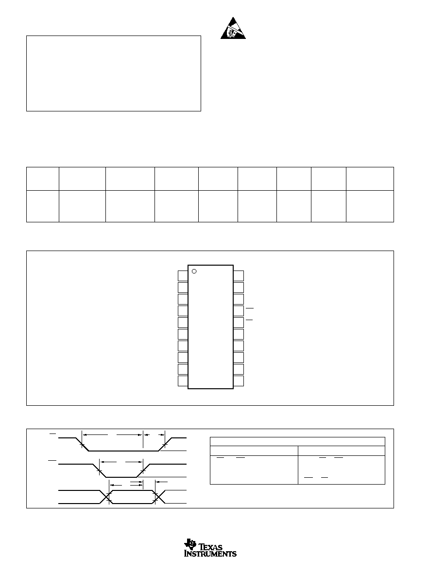
UNIPOLAR OPERATION
Figure 2 shows the DAC7545 connected for unipolar opera-
tion. The high-grade DAC7545 is specified for a 1LSB gain
error, so gain adjust is typically not needed; however, the
resistors shown are for adjusting full-scale errors. The value
of R
1
should be minimized to reduce the effects of mismatch-
ing temperature coefficients between the internal and exter-
nal resistors. A range of adjustment of 1.5 times the desired
range will be adequate. For example, for a DAC7545JP, the
gain error is specified to be
±
25LSB, therefore, a range of
adjustment of
±
37LSB will be adequate. Equation 1 results in
a value of 458W for the potentiometer (use 500
).
R
R
Gain Error
LADDER
1
4096
3
=
(
)
∑
(1)
FIGURE 2. Unipolar Binary Operation.
BINARY CODE
ANALOG OUTPUT
MSB
LSB
1111 1111 1111
≠V
IN
(4095/4096)
1000 0000 0000
≠V
IN
(2048/4096) = ≠1/2V
IN
0000 0000 0001
≠V
IN
(1/4096)
0000 0000 0000
0V
TABLE I. Unipolar Codes.
OPA604
V
IN
R
1
R
2
V
DD
R
FB
DAC7545 AGND
DGND
OUT 1
DB
0
-DB
11
C
1
33pF
+5V
V
OUT
V
REF
R
3
, R
4
, and R
5
must match within 0.01% and must be the
same type of resistors (preferably wire-wound or metal foil),
so that the temperature coefficients match; mismatch of R
3
value to R
4
causes both offset and full-scale error. Mismatch
of R
5
to R
4
and R
3
causes full-scale error.
FIGURE 3. Bipolar Operation (binary two's complement code).
OPA604
or
1/2 OPA2604
V
IN
R
1
R
2
V
DD
R
FB
DAC7545
AGND
DB
10
-DB
0
OUT 1
Data Input
C
1
33pF
+5V
DB
11
V
REF
V
OUT
R
3
10k
R
4
20k
R
5
20k
R
6
5k
10%
U
1
(see text)
12
11
Analog Common
2
1
18
20
19
4
OPA604
or
1/2 OPA2604
DATA INPUT
ANALOG OUTPUT
MSB
LSB
0111 1111 1111
+V
IN
(2047/2048)
0000 0000 0001
+V
IN
(1/2048)
0000 0000 0000
0V
1111 1111 1111
≠V
IN
(1/2048)
1000 0000 0000
≠V
IN
(2048/2048)
TABLE II. Binary Two's Complement Code Table for Circuit
of Figure 3.
tance. Eliminating this capacitor will result in excessive ringing
and an increase in glitch energy, therefore, this capacitor must
be as small as possible to minimize settling time.
The circuit of Figure 2 can be used with input voltages up to
±
20V as long as the output amplifier is biased to handle the
excursions. Table I represents the analog output for four
codes into the DAC for Figure 2.
BIPOLAR OPERATION
Figure 3 and Table II illustrate the recommended circuit and
code relationship for bipolar operation. The DAC function uses
offset binary code. The inverter, U
1
, on the MSB line converts
binary two's complement input code to offset binary code. If the
inversion is done in software, U
1
can be omitted.
The addition of R
1
will cause a negative gain error. To
compensate for this error, R
2
must be added. The value of R
2
should be one-third the value of R
1
.
The capacitor across the feedback resistor is used to compen-
sate for the phase shift due to stray capacitances of the circuit
board, the DAC output capacitance, and op amp input capaci-
DAC7545
6
SBAS150A
www.ti.com
FIGURE 5. 8-Bit Processor Interface.
DAC7545
CS
DB
0
DB
7
WR
DB
8
DB
11
Latch
CS
WR
4
4
8
Q
1
(2)
8-Bit Data Bus
Q
0
(1)
Address Bus
Address
Decode
CPU
WR
DB
7
DB
0
A
15
A
0
NOTES: (1) Q
0
= decoded address for DAC.
(2) Q
1
= decoded address for latch.
FIGURE 4. Digitally Controlled Gain Block.
R
FB
DAC7545
AGND
DGND
OUT
1
DB
0
-DB
11
V
IN
WR
V
OUT
CS
16
+5V
NOTE: There must be
at least 1LSB loaded in
the DAC or the amp will
saturate due to the lack
of feedback.
OPA111
17
18
19
V
OUT
=
≠V
IN
DB
11
+
2
DB
10
+
4
DB
9
+ ∑∑∑ +
8
DB
0
4096
20
DIGITALLY-CONTROLLED GAIN BLOCK
Figure 4 shows a circuit for a digitally-controlled gain block.
The feedback for the op amp is made up of the FET switch
and the R-2R ladder. The input resistor to the gain block is
the R
FB
of the DAC7545. As the FET switch is in the
feedback loop, a zero code into the DAC will result in the op
amp having no feedback, and a saturated op amp output.
APPLICATION HINTS
CMOS DACs, such as the DAC7545, exhibit a code-depen-
dent out resistance. The effect of this is a code-dependent
differential nonlinearity at the amplifier output that depends on
the offset voltage, V
OS
, of the amplifier. Thus linearity depends
upon the potential of OUT 1 and AGND being exactly equal to
each other. Usually the DAC is connected to an external op
amp with the noninverting input connected to AGND. The op
amp selected should have a low input bias current and low V
OS
and V
OS
drift over temperature. The op amp offset voltage
should be less than (25 ∑ 10
≠6
)(V
REF
) over operating conditions.
Suitable op amps are the OPA37 and the OPA627 for fixed
reference applications and low-bandwidth requirement; the
OPA37 has low V
OS
and does not require an offset trim. For
wide bandwidth, high slew rate, or fast-settling applications, the
OPA604 or 1/2 OPA2604 are recommended.
Unused digital inputs must be connected to V
DD
or to DGND,
this prevents noise from triggering the high impedance digital
input. It is suggested that the unused digital inputs also be
given a path to ground or V
DD
through a 1mW resistor to
prevent the accumulation of static charge if the PC card is
unplugged from the system. In addition, in systems where
the AGND to DGND connection is on a backplane, it is
recommended that two diodes be connected in inverse
parallel between AGND and DGND.
INTERFACING
TO MICROPROCESSORS
The DAC7545 can be directly interfaced to either an 8- or 16-
bit microprocessor through its 12-bit wide data latch using
the CS and WR controls.
An 8-bit processor interface is shown in Figure 5. It uses two
memory addresses: one for the lower 8 bits and one for the
upper 4 bits of data into the DAC via the latch.

DAC7545
7
SBAS150A
www.ti.com
PACKAGE DRAWING
DW (R-PDSO-G**)
PLASTIC SMALL-OUTLINE PACKAGE
16 PINS SHOWN
4040000 / E 08/01
Seating Plane
0.400 (10,15)
0.419 (10,65)
0.104 (2,65) MAX
1
0.012 (0,30)
0.004 (0,10)
A
8
16
0.020 (0,51)
0.014 (0,35)
0.291 (7,39)
0.299 (7,59)
9
0.010 (0,25)
0.050 (1,27)
0.016 (0,40)
(15,24)
(15,49)
PINS **
0.010 (0,25) NOM
A MAX
DIM
A MIN
Gage Plane
20
0.500
(12,70)
(12,95)
0.510
(10,16)
(10,41)
0.400
0.410
16
0.600
24
0.610
(17,78)
28
0.700
(18,03)
0.710
0.004 (0,10)
M
0.010 (0,25)
0.050 (1,27)
0
∞
≠ 8
∞
(11,51)
(11,73)
0.453
0.462
18
NOTES: A. All linear dimensions are in inches (millimeters).
B. This drawing is subject to change without notice.
C. Body dimensions do not include mold flash or protrusion not to exceed 0.006 (0,15).
D. Falls within JEDEC MS-013

PACKAGING INFORMATION
ORDERABLE DEVICE
STATUS(1)
PACKAGE TYPE
PACKAGE DRAWING
PINS
PACKAGE QTY
DAC7545GLP
NRND
ZZ (BB)
ZZ222
20
DAC7545GLU
ACTIVE
SOIC
DW
20
38
DAC7545JP
NRND
ZZ (BB)
ZZ222
20
DAC7545JU
ACTIVE
SOIC
DW
20
38
DAC7545KP
NRND
ZZ (BB)
ZZ222
20
DAC7545KU
ACTIVE
SOIC
DW
20
38
DAC7545LP
NRND
ZZ (BB)
ZZ222
20
DAC7545LU
ACTIVE
SOIC
DW
20
38
(1) The marketing status values are defined as follows:
ACTIVE: Product device recommended for new designs.
LIFEBUY: TI has announced that the device will be discontinued, and a lifetime-buy period is in effect.
NRND: Not recommended for new designs. Device is in production to support existing customers, but TI does not recommend using this part in
a new design.
PREVIEW: Device has been announced but is not in production. Samples may or may not be available.
OBSOLETE: TI has discontinued the production of the device.
PACKAGE OPTION ADDENDUM
www.ti.com
3-Oct-2003

IMPORTANT NOTICE
Texas Instruments Incorporated and its subsidiaries (TI) reserve the right to make corrections, modifications,
enhancements, improvements, and other changes to its products and services at any time and to discontinue
any product or service without notice. Customers should obtain the latest relevant information before placing
orders and should verify that such information is current and complete. All products are sold subject to TI's terms
and conditions of sale supplied at the time of order acknowledgment.
TI warrants performance of its hardware products to the specifications applicable at the time of sale in
accordance with TI's standard warranty. Testing and other quality control techniques are used to the extent TI
deems necessary to support this warranty. Except where mandated by government requirements, testing of all
parameters of each product is not necessarily performed.
TI assumes no liability for applications assistance or customer product design. Customers are responsible for
their products and applications using TI components. To minimize the risks associated with customer products
and applications, customers should provide adequate design and operating safeguards.
TI does not warrant or represent that any license, either express or implied, is granted under any TI patent right,
copyright, mask work right, or other TI intellectual property right relating to any combination, machine, or process
in which TI products or services are used. Information published by TI regarding third-party products or services
does not constitute a license from TI to use such products or services or a warranty or endorsement thereof.
Use of such information may require a license from a third party under the patents or other intellectual property
of the third party, or a license from TI under the patents or other intellectual property of TI.
Reproduction of information in TI data books or data sheets is permissible only if reproduction is without
alteration and is accompanied by all associated warranties, conditions, limitations, and notices. Reproduction
of this information with alteration is an unfair and deceptive business practice. TI is not responsible or liable for
such altered documentation.
Resale of TI products or services with statements different from or beyond the parameters stated by TI for that
product or service voids all express and any implied warranties for the associated TI product or service and
is an unfair and deceptive business practice. TI is not responsible or liable for any such statements.
Following are URLs where you can obtain information on other Texas Instruments products and application
solutions:
Products
Applications
Amplifiers
amplifier.ti.com
Audio
www.ti.com/audio
Data Converters
dataconverter.ti.com
Automotive
www.ti.com/automotive
DSP
dsp.ti.com
Broadband
www.ti.com/broadband
Interface
interface.ti.com
Digital Control
www.ti.com/digitalcontrol
Logic
logic.ti.com
Military
www.ti.com/military
Power Mgmt
power.ti.com
Optical Networking
www.ti.com/opticalnetwork
Microcontrollers
microcontroller.ti.com
Security
www.ti.com/security
Telephony
www.ti.com/telephony
Video & Imaging
www.ti.com/video
Wireless
www.ti.com/wireless
Mailing Address:
Texas Instruments
Post Office Box 655303 Dallas, Texas 75265
Copyright
2003, Texas Instruments Incorporated