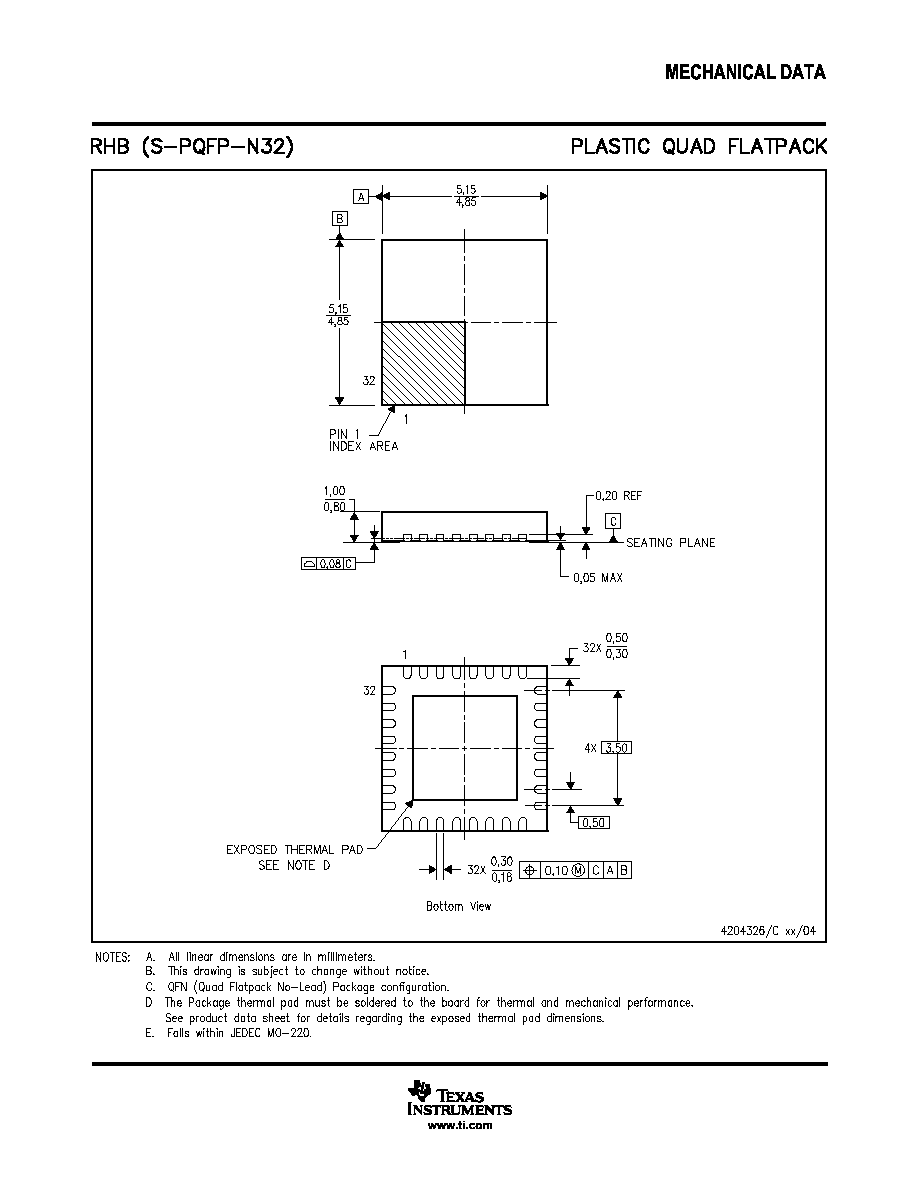
www.ti.com
FEATURES
DESCRIPTION
APPLICATIONS
Input
Register
Input
Register
DAC
Register
DAC
Register
String
DAC A
String
DAC H
Interface
Logic
Power-On
Reset
Power-Down
Logic
+
IOV
DD
VREF2
SCLK
SYNC
SDIN
V
OUT
A
V
OUT
H
SDO
RST RSTSEL
AGND
DGND VREF3
VREF4
PD
-
VFBA
+
-
VFBH
VREF1
V
DD
DCEN
DAC7558
SLAS435 ≠ MAY 2005
12-BIT, OCTAL, ULTRALOW GLITCH, VOLTAGE OUTPUT
DIGITAL-TO-ANALOG CONVERTER
∑
2.7-V to 5.5-V Single Supply
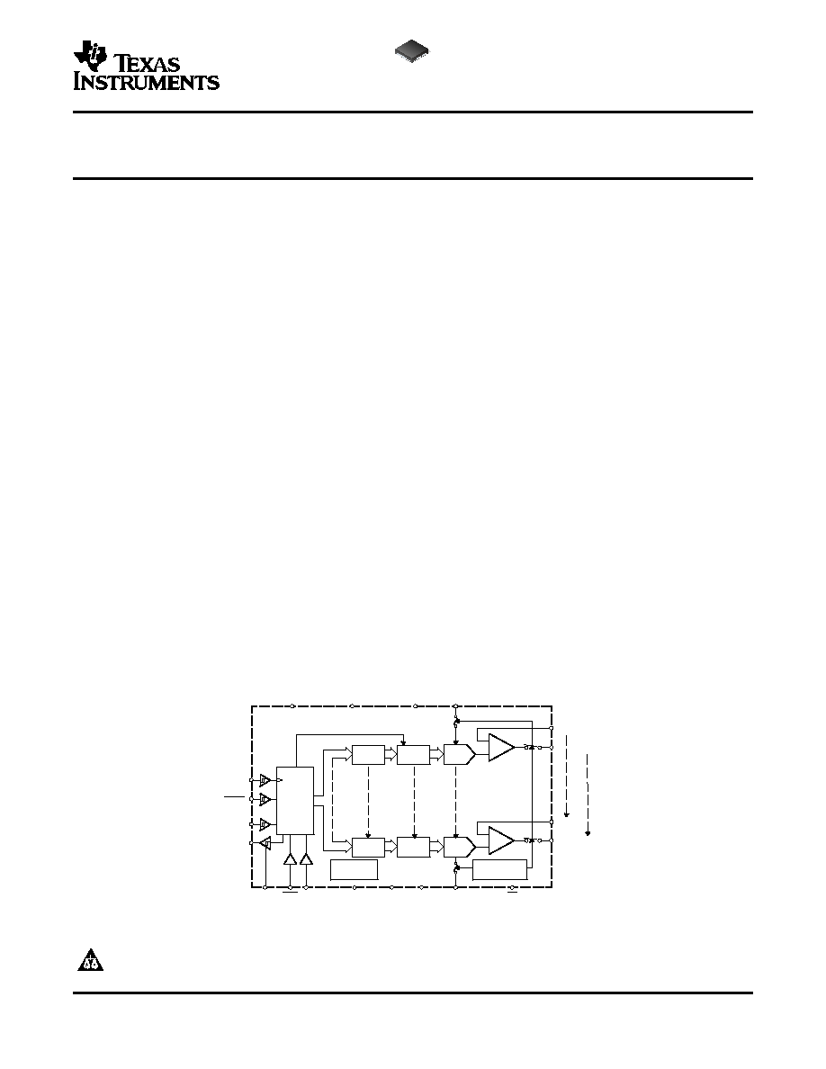
The DAC7558 is a 12-bit, octal-channel, voltage
output
DAC
with
exceptional
linearity
and
∑
12-Bit Linearity and Monotonicity
monotonicity. Its proprietary architecture minimizes
∑
Rail-to-Rail Voltage Output
undesired transients such as code to code glitch and
∑
Settling Time: 5 µs (Max)
channel
to
channel
crosstalk.
The
low-power
∑
Ultralow Glitch Energy: 0.1 nVs
DAC7558 operates from a single 2.7-V to 5.5-V
supply. The DAC7558 output amplifiers can drive a
∑
Ultralow Crosstalk: ≠100 dB
2-k
, 200-pF load rail-to-rail with 5-µs settling time;
∑
Low Power: 1.8 mA (Max)
the output range is set using an external voltage
∑
Per-Channel Power Down: 2 µA (Max)
reference.
∑
Power-On Reset to Zero Scale and Mid Scale
The 3-wire serial interface operates at clock rates up
∑
SPI-Compatible Serial Interface: Up to 50 MHz
to 50 MHz and is compatible with SPI, QSPI,
MicrowireTM, and DSP interface standards. The out-
∑
Simultaneous or Sequential Update
puts of all DACs may be updated simultaneously or
∑
Asynchronous Clear
sequentially. The parts incorporate a power-on-reset
∑
Binary and Twos-Complement Capability
circuit to ensure that the DAC outputs power up to
zero volts and remain there until a valid write cycle to
∑
Daisy-Chain Operation
the
device
takes
place.
The
parts
contain
a
∑
1.8-V to 5.5-V Logic Compatibility
power-down feature that reduces the current con-
∑
Specified Temperature Range: ≠40∞C to 105∞C
sumption of the device to under 2 µA.
∑
Small, 5-mm x 5-mm, 32-Lead QFN Package
The small size and low-power operation makes the
DAC7558 ideally suited for battery-operated portable
applications. The power consumption is typically 7.5
mW at 5 V, 3.7 mW at 3 V, and reduces to 1 µW in
∑
Portable Battery-Powered Instruments
power-down mode.
∑
Digital Gain and Offset Adjustment
∑
Programmable Voltage and Current Sources
The DAC7558 is available in a 32-lead QFN package
and is specified over ≠40∞C to 105∞C.
∑
Programmable Attenuators
∑
Industrial Process Control
FUNCTIONAL BLOCK DIAGRAM
Please be aware that an important notice concerning availability, standard warranty, and use in critical applications of Texas
Instruments semiconductor products and disclaimers thereto appears at the end of this data sheet.
Microwire is a trademark of National Semiconductor Corp..
PRODUCTION DATA information is current as of publication date.
Copyright © 2005, Texas Instruments Incorporated
Products conform to specifications per the terms of the Texas
Instruments standard warranty. Production processing does not
necessarily include testing of all parameters.

www.ti.com
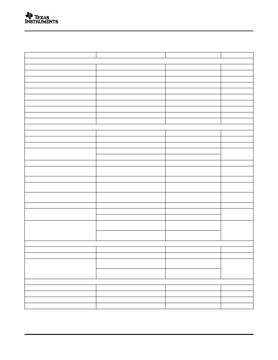
ABSOLUTE MAXIMUM RATINGS
DAC7558
SLAS435 ≠ MAY 2005
This integrated circuit can be damaged by ESD. Texas Instruments recommends that all integrated
circuits be handled with appropriate precautions. Failure to observe proper handling and installation
procedures can cause damage.
ESD damage can range from subtle performance degradation to complete device failure. Precision
integrated circuits may be more susceptible to damage because very small parametric changes could
cause the device not to meet its published specifications.
ORDERING INFORMATION
(1)
SPECIFIED
PACKAGE
PACKAGE
ORDERING
TRANSPORT
PRODUCT
PACKAGE
TEMPERATURE
DESIGNATOR
MARKING
NUMBER
MEDIA
RANGE
DAC7558IRHBT
250-piece Tape and
Reel
DAC7558
32 QFN
RHB
≠40∞C TO 105∞C
D758
DAC7558IRHBR
3000-piece Tape
and Reel
(1)
For the most current package and ordering information, see the Package Option Addendum at the end of this document, or see the TI
Web site at
www.ti.com
.
over operating free-air temperature range (unless otherwise noted)
(1)
UNIT
V
DD
to GND
≠0.3 V to 6 V
Digital input voltage to GND
≠0.3 V to V
DD
+ 0.3 V
V
out
to GND
≠0.3 V to V
DD
+ 0.3 V
Operating temperature range
≠40∞C to 105∞C
Storage temperature range
≠65∞C to 150∞C
Junction temperature (T
J
Max)
150∞C
(1)
Stresses above those listed under "Absolute Maximum Ratings" may cause permanent damage to the device. Exposure to absolute
maximum conditions for extended periods may affect device reliability.
2
www.ti.com
ELECTRICAL CHARACTERISTICS
DAC7558
SLAS435 ≠ MAY 2005
V
DD
= 2.7 V to 5.5 V, VREF = VDD, R
L
= 2 k
to GND; C
L
= 200 pF to GND; all specifications ≠40∞C to 105∞C, unless
otherwise specified
PARAMETER
TEST CONDITIONS
MIN
TYP
MAX
UNITS
STATIC PERFORMANCE
(1)
Resolution
12
Bits
Relative accuracy
±0.35
±1
LSB
Differential nonlinearity
Specified monotonic by design
±0.08
±0.5
LSB
Offset error
±12
mV
Zero-scale error
All zeroes loaded to DAC register
±12
mV
Gain error
V
DD
= 5 V, V
REF
= 4.096 V
±0.15
%FSR
Full-scale error
V
DD
= 5 V, V
REF
= 4.096 V
±0.5
%FSR
Zero-scale error drift
7
µV/∞C
Gain temperature coefficient
3
ppm of FSR/∞C
PSRR
V
DD
= 5 V
0.75
mV/V
OUTPUT CHARACTERISTICS
(2)
Output voltage range
0
VREF
V
Output voltage settling time
R
L
= 2 k
; 0 pF < C
L
< 200 pF
5
µs
Slew rate
1.8
V/µs
Capacitive load stability
R
L
=
470
pF
R
L
= 2 k
1000
Digital-to-analog glitch impulse
1 LSB change around major carry
0.1
nV-s
Channel-to-channel crosstalk
1-kHz full-scale sine wave,
≠100
dB
outputs unloaded
Digital feedthrough
0.1
nV-s
Output noise density (10-kHz offset
120
nV/rtHz
frequency)
Total harmonic distortion
F
OUT
= 1 kHz, F
S
= 1 MSPS, BW = 20
≠85
dB
kHz
DC output impedance
1
Short-circuit current
V
DD
= 5 V
50
mA
V
DD
= 3 V
20
Power-up time
Coming out of power-down mode,
15
µs
V
DD
= 5 V
Coming out of power-down mode,
15
V
DD
= 3 V
REFERENCE INPUT
V
REF
Input range
0
V
DD
V
Reference input impedance
V
REF
1 through V
REF
4 shorted together
12.5
k
Reference current
V
REF
= V
DD
= 5 V,
400
650
µA
V
REF
1 through V
REF
4 shorted together
V
REF
= V
DD
= 3 V,
240
425
V
REF
1 through V
REF
4 shorted together
LOGIC INPUTS
(2)
Input current
±1
µA
V
IN_L
, Input low voltage
IOV
DD
2.7 V
0.3 IOV
DD
V
V
IN_H
, Input high voltage
IOV
DD
2.7 V
0.7 IOV
DD
V
Pin capacitance
3
pF
(1)
Linearity tested using a reduced code range of 30 to 4065; output unloaded.
(2)
Specified by design and characterization, not production tested. For 1.8 V < IOV
DD
< 2.7 V, it is recommended that V
IH
= IOV
DD
, V
IL
=
GND.
3
www.ti.com
ELECTRICAL CHARACTERISTICS (Continued)
DAC7558
SLAS435 ≠ MAY 2005
V
DD
= 2.7 V to 5.5 V, VREF = VDD, R
L
= 2 k
to GND; C
L
= 200 pF to GND; all specifications ≠40∞C to 105∞C, unless
otherwise specified
PARAMETER
TEST CONDITIONS
MIN
TYP
MAX
UNITS
POWER REQUIREMENTS
V
DD
, IOV
DD
(1)
2.7
5.5
V
I
DD
(normal operation)
DAC active and excluding load current
V
DD
= 3.6 V to 5.5 V
1.1
1.8
mA
V
IH
= IOV
DD
and V
IL
= GND
V
DD
= 2.7 V to 3.6 V
1
1.7
I
DD
(all power-down modes)
V
DD
= 3.6 V to 5.5 V
V
IH
= IOV
DD
and V
IL
= GND
0.2
2
µA
V
DD
= 2.7 V to 3.6 V
0.05
2
POWER EFFICIENCY
I
OUT
/I
DD
I
LOAD
= 2 mA, V
DD
= 5 V
93%
(1)
IOV
DD
operates down to 1.8 V with slightly degraded timing, as long as V
IH
= IOV
DD
and V
IL
= GND.
4
www.ti.com
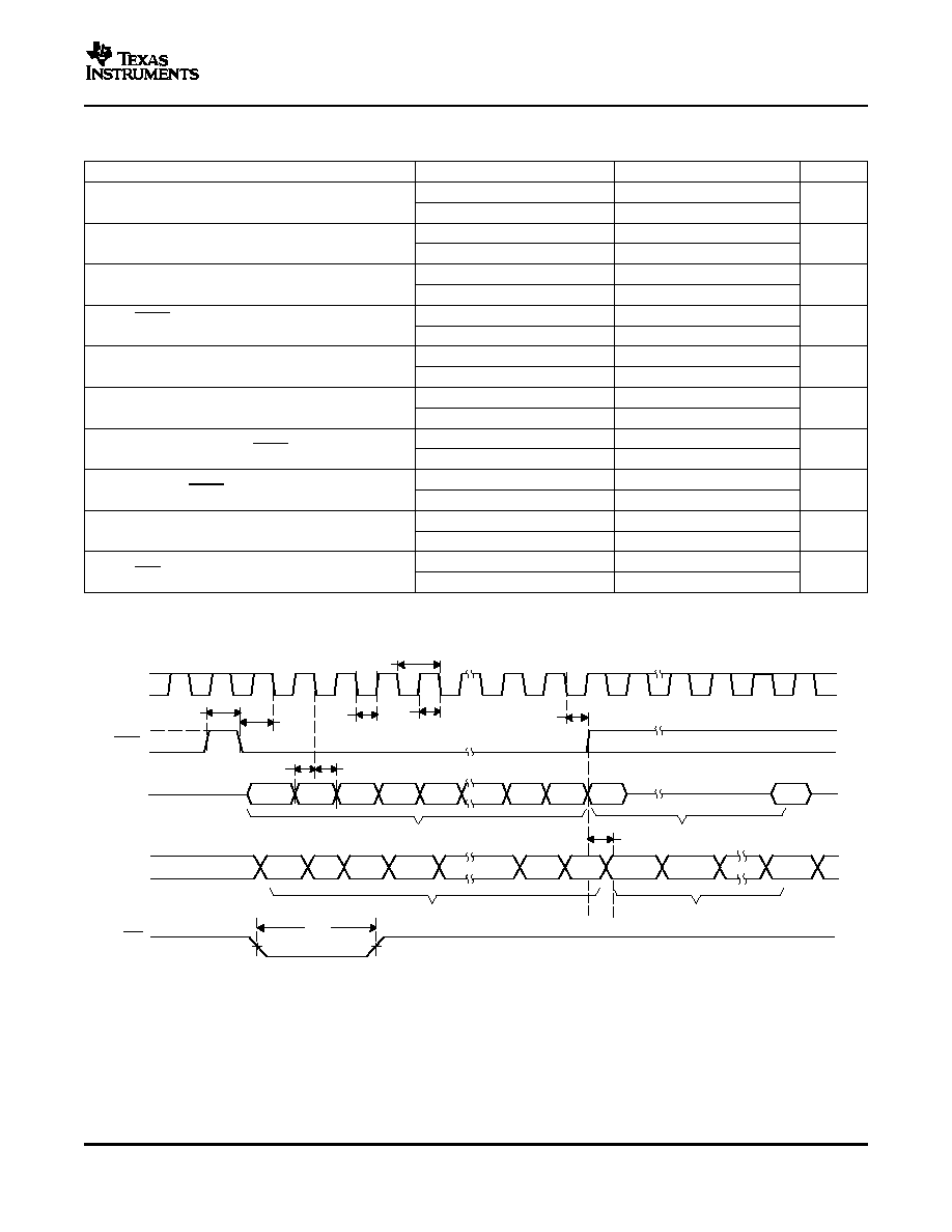
TIMING CHARACTERISTICS
(1) (2)
SCLK
SYNC
SDIN
D23
D22
D21
D20
D19
D1
D0
D23
t
8
t
4
t
3
t
2
t
1
t
7
t
6
t
5
D0
t
9
Input Word n
Input Word n+1
Undefined
D23
D22
D0
Input Word n
t
10
SDO
CLR
DAC7558
SLAS435 ≠ MAY 2005
V
DD
= 2.7 V to 5.5 V, R
L
= 2 k
to GND; all specifications ≠40∞C to 105∞C, unless otherwise specified
PARAMETER
TEST CONDITIONS
MIN
TYP
MAX
UNITS
V
DD
= 2.7 V to 3.6 V
20
t
1
(3)
SCLK cycle time
ns
V
DD
= 3.6 V to 5.5 V
20
V
DD
= 2.7 V to 3.6 V
10
t
2
SCLK HIGH time
ns
V
DD
= 3.6 V to 5.5 V
10
V
DD
= 2.7 V to 3.6 V
10
t
3
SCLK LOW time
ns
V
DD
= 3.6 V to 5.5 V
10
V
DD
= 2.7 V to 3.6 V
4
SYNC falling edge to SCLK falling edge setup
t
4
ns
time
V
DD
= 3.6 V to 5.5 V
4
V
DD
= 2.7 V to 3.6 V
5
t
5
Data setup time
ns
V
DD
= 3.6 V to 5.5 V
5
V
DD
= 2.7 V to 3.6 V
4.5
t
6
Data hold time
ns
V
DD
= 3.6 V to 5.5 V
4.5
V
DD
= 2.7 V to 3.6 V
0
t
7
SCLK falling edge to SYNC rising edge
ns
V
DD
= 3.6 V to 5.5 V
0
V
DD
= 2.7 V to 3.6 V
20
t
8
Minimum SYNC HIGH time
ns
V
DD
= 3.6 V to 5.5 V
20
V
DD
= 2.7 V to 3.6 V
10
t
9
SCLK falling edge to SDO valid
ns
V
DD
= 3.6 V to 5.5 V
10
V
DD
= 2.7 V to 3.6 V
10
t
10
CLR pulse width low
ns
V
DD
= 3.6 V to 5.5 V
10
(1)
All input signals are specified with t
R
= t
F
= 1 ns (10% to 90% of V
DD
) and timed from a voltage level of (V
IL
+ V
IH
)/2.
(2)
See Serial Write Operation timing diagram
Figure 1
.
(3)
Maximum SCLK frequency is 50 MHz at V
DD
= 2.7 V to 5.5 V.
Figure 1. Serial Write Operation
5
www.ti.com
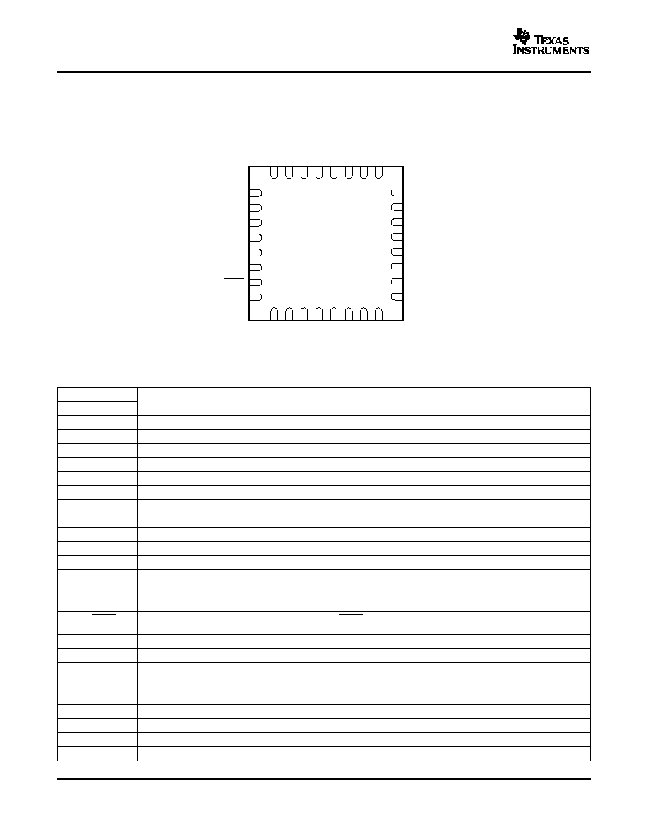
PIN DESCRIPTION
25
26
27
28
29
30
31
32
1
2
3
4
5
6
7
8
16
15
14
13
12
11
10
9
24 23 22 21 20 19 18 17
VREF4
DCEN
PD
VDD
AGND
RSTSEL
RST
VREF1
VREF3
SYNC
SCLK
SDIN
DGND
IOVDD
SDO
VREF2
VFBH
VFBA
VOUT
A
VOUTB
VFBB
VFBC
VOUTC
VOUTD
VFBD
VOUTH
VOUTG
VFBG
VFBF
VOUTF
VOUTE
VFBE
RHB PACKAGE
(TOP VIEW)
DAC7558
SLAS435 ≠ MAY 2005
Terminal Functions
TERMINAL
DESCRIPTION
NO.
NAME
1
VFBA
DAC A amplifier sense input
2
VOUTA
Analog output voltage from DAC A
3
VOUTB
Analog output voltage from DAC B
4
VFBB
DAC B amplifier sense input
5
VFBC
DAC C amplifier sense input
6
VOUTC
Analog output voltage from DAC C
7
VOUTD
Analog output voltage from DAC D
8
VFBD
DAC D amplifier sense input
9
VREF2
Positive reference voltage input for DAC C and DAC D
10
SDO
Serial data output
11
IOVDD
I/O voltage supply input
12
DGND
Digital ground
13
SDIN
Serial data input
14
SCLK
Serial clock input
15
SYNC
Frame synchronization input. The falling edge of the SYNC pulse indicates the start of a serial data frame shifted out
to the DAC7558.
16
VREF3
Positive reference voltage input for DAC E and DAC F
17
VFBE
DAC E amplifier sense input
18
VOUTE
Analog output voltage from DAC E
19
VOUTF
Analog output voltage from DAC F
20
VFBF
DAC F amplifier sense input
21
VFBG
DAC G amplifier sense input
22
VOUTG
Analog output voltage from DAC G
23
VOUTH
Analog output voltage from DAC H
24
VFBH
DAC H amplifier sense input
6
www.ti.com
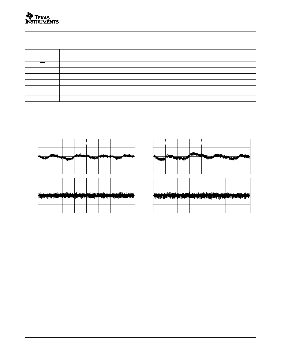
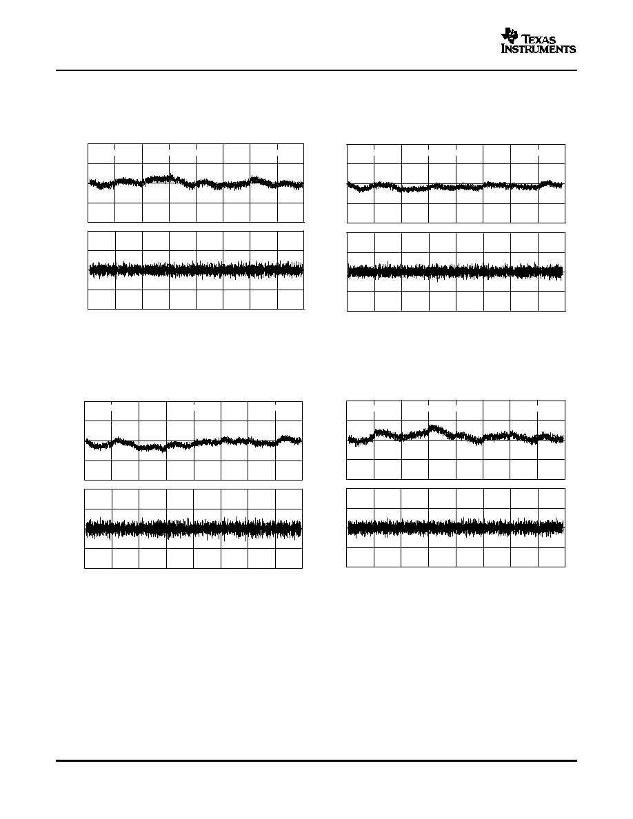
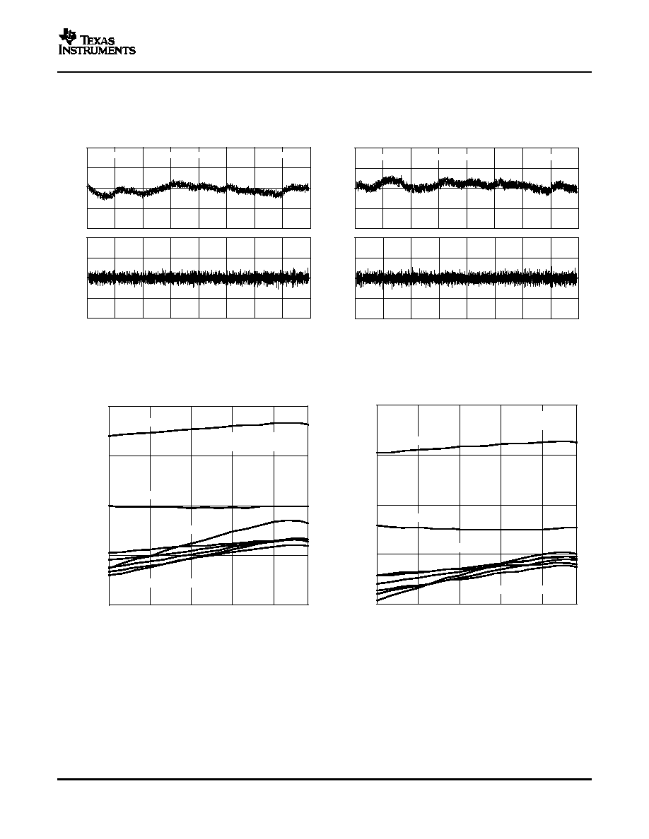
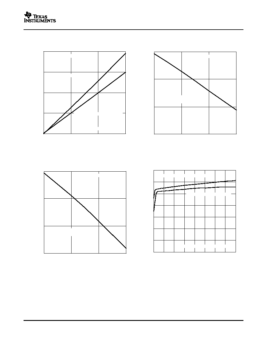
TYPICAL CHARACTERISTICS
-1
-0.5
0
0.5
1
Linearity Error - LSB
-0.5
-0.25
0
0.25
0.5
0
512
1024
1536
2048
2560
3072
3584
4096
Digital Input Code
Differential Linearity Error - LSB
Channel A
V
REF
= 4.096 V
V
DD
= 5 V
-1
-0.5
0
0.5
1
-0.5
-0.25
0
0.25
0.5
0
512
1024
1536
2048
2560
3072
3584
4096
Digital Input Code
Linearity Error - LSB
Differential Linearity Error - LSB
Channel B
V
REF
= 4.096 V
V
DD
= 5 V
DAC7558
SLAS435 ≠ MAY 2005
PIN DESCRIPTION (continued)
Terminal Functions (continued)
25
VREF4
Positive reference voltage input for DAC G and DAC H
26
DCEN
Daisy-chain enable
27
PD
Power down
28
VDD
Analog voltage supply input
29
AGND
Analog ground
30
RSTSEL
Reset select. If this pin is low, input coding is binary; if high, then 2s compliment.
31
RST
Asynchronous reset. Active low. If RST pin is low, all DAC channels reset either to zero scale (RSTSEL = 0) or to
midscale (RSTSEL = 1).
32
VREF1
Positive reference voltage input for DAC A and DAC B
LINEARITY ERROR AND
LINEARITY ERROR AND
DIFFERENTIAL LINEARITY ERROR
DIFFERENTIAL LINEARITY ERROR
vs
vs
DIGITAL INPUT CODE
DIGITAL INPUT CODE
Figure 2.
Figure 3.
7
www.ti.com
-1
-0.5
0
0.5
1
-0.5
-0.25
0
0.25
0.5
0
512
1024
1536
2048
2560
3072
3584
4096
Digital Input Code
Linearity Error - LSB
Differential Linearity Error - LSB
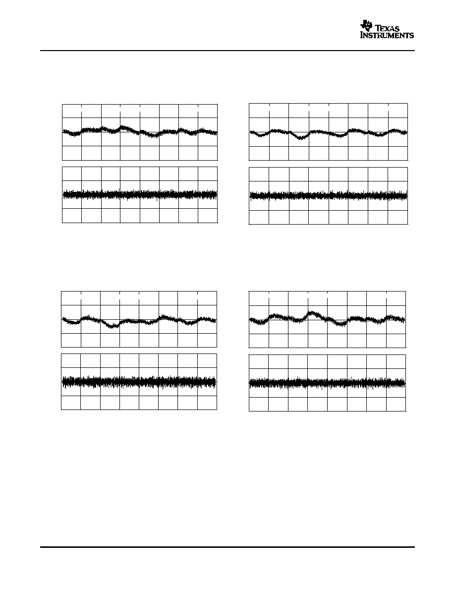
Channel C
V
REF
= 4.096 V
V
DD
= 5 V
-1
-0.5
0
0.5
1
-0.5
-0.25
0
0.25
0.5
0
512
1024
1536
2048
2560
3072
3584
4096
Digital Input Code
Linearity Error - LSB
Differential Linearity Error - LSB
Channel D
V
REF
= 4.096 V
V
DD
= 5 V
-1
-0.5
0
0.5
1
-0.5
-0.25
0
0.25
0.5
0
512
1024
1536
2048
2560
3072
3584
4096
Digital Input Code
Linearity Error - LSB
Differential Linearity Error - LSB
Channel E
V
REF
= 4.096 V
V
DD
= 5 V
-1
-0.5
0
0.5
1
-0.5
-0.25
0
0.25
0.5
0
512
1024
1536
2048
2560
3072
3584
4096
Digital Input Code
Linearity Error - LSB
Differential Linearity Error - LSB
Channel F
V
REF
= 4.096 V
V
DD
= 5 V
DAC7558
SLAS435 ≠ MAY 2005
TYPICAL CHARACTERISTICS (continued)
LINEARITY ERROR AND
LINEARITY ERROR AND
DIFFERENTIAL LINEARITY ERROR
DIFFERENTIAL LINEARITY ERROR
vs
vsDIGITAL INPUT CODE
DIGITAL INPUT CODE
Figure 4.
Figure 5.
LINEARITY ERROR AND
LINEARITY ERROR AND
DIFFERENTIAL LINEARITY ERROR
DIFFERENTIAL LINEARITY ERROR
vs
vs
DIGITAL INPUT CODE
DIGITAL INPUT CODE
Figure 6.
Figure 7.
8
www.ti.com
-1
-0.5
0
0.5
1
-0.5
-0.25
0
0.25
0.5
0
512
1024
1536
2048
2560
3072
3584
4096
Digital Input Code
Linearity Error - LSB
Differential Linearity Error - LSB
Channel H
V
REF
= 4.096 V
V
DD
= 5 V
-1
-0.5
0
0.5
1
-0.5
-0.25
0
0.25
0.5
0
512
1024
1536
2048
2560
3072
3584
4096
Digital Input Code
Linearity Error - LSB
Differential Linearity Error - LSB
Channel G
V
REF
= 4.096 V
V
DD
= 5 V
-1
-0.5
0
0.5
1
-0.5
-0.25
0
0.25
0.5
0
512
1024
1536
2048
2560
3072
3584
4096
Digital Input Code
Linearity Error - LSB
Differential Linearity Error - LSB
Channel A
V
REF
= 2.5 V
V
DD
= 2.7 V
-1
-0.5
0
0.5
1
-0.5
-0.25
0
0.25
0.5
0
512
1024
1536
2048
2560
3072
3584
4096
Digital Input Code
Linearity Error - LSB
Differential Linearity Error - LSB
Channel B
V
REF
= 2.5 V
V
DD
= 2.7 V
DAC7558
SLAS435 ≠ MAY 2005
TYPICAL CHARACTERISTICS (continued)
LINEARITY ERROR AND
LINEARITY ERROR AND
DIFFERENTIAL LINEARITY ERROR
DIFFERENTIAL LINEARITY ERROR
vs
vs
DIGITAL INPUT CODE
DIGITAL INPUT CODE
Figure 8.
Figure 9.
LINEARITY ERROR AND
LINEARITY ERROR AND
DIFFERENTIAL LINEARITY ERROR
DIFFERENTIAL LINEARITY ERROR
vs
vs
DIGITAL INPUT CODE
DIGITAL INPUT CODE
Figure 10.
Figure 11.
9
www.ti.com
-1
-0.5
0
0.5
1
-0.5
-0.25
0
0.25
0.5
0
512
1024
1536
2048
2560
3072
3584
4096
Digital Input Code
Linearity Error - LSB
Differential Linearity Error - LSB
Channel C
V
REF
= 2.5 V
V
DD
= 2.7 V
-1
-0.5
0
0.5
1
-0.5
-0.25
0
0.25
0.5
0
512
1024
1536
2048
2560
3072
3584
4096
Digital Input Code
Linearity Error - LSB
Differential Linearity Error - LSB
Channel D
V
REF
= 2.5 V
V
DD
= 2.7 V
-1
-0.5
0
0.5
1
-0.5
-0.25
0
0.25
0.5
0
512
1024
1536
2048
2560
3072
3584
4096
Digital Input Code
Linearity Error - LSB
Differential Linearity Error - LSB
Channel E
V
REF
= 2.5 V
V
DD
= 2.7 V
-1
-0.5
0
0.5
1
-0.5
-0.25
0
0.25
0.5
0
512
1024
1536
2048
2560
3072
3584
4096
Digital Input Code
Linearity Error - LSB
Differential Linearity Error - LSB
Channel F
V
REF
= 2.5 V
V
DD
= 2.7 V
DAC7558
SLAS435 ≠ MAY 2005
TYPICAL CHARACTERISTICS (continued)
LINEARITY ERROR AND
LINEARITY ERROR AND
DIFFERENTIAL LINEARITY ERROR
DIFFERENTIAL LINEARITY ERROR
vs
vs
DIGITAL INPUT CODE
DIGITAL INPUT CODE
Figure 12.
Figure 13.
LINEARITY ERROR AND
LINEARITY ERROR AND
DIFFERENTIAL LINEARITY ERROR
DIFFERENTIAL LINEARITY ERROR
vs
vs
DIGITAL INPUT CODE
DIGITAL INPUT CODE
Figure 14.
Figure 15.
10
www.ti.com
-1
-0.5
0
0.5
1
-0.5
-0.25
0
0.25
0.5
0
512
1024
1536
2048
2560
3072
3584
4096
Digital Input Code
Linearity Error - LSB
Differential Linearity Error - LSB
Channel G
V
REF
= 2.5 V
V
DD
= 2.7 V
-1
-0.5
0
0.5
1
-0.5
-0.25
0
0.25
0.5
0
512
1024
1536
2048
2560
3072
3584
4096
Digital Input Code
Linearity Error - LSB
Differential Linearity Error - LSB
Channel H
V
REF
= 2.5 V
V
DD
= 2.7 V
-4
-2
0
2
4
-40
-10
20
50
80
CHE
CHD
CHF
CHA, B, C, G, H
V
DD
= 2.7 V,
V
REF
= 2.5 V
Zero-Scale Error - mV
T
A
- Free-Air Temperature -
5
C
-4
-2
0
2
4
-40
-10
20
50
80
CHE
CHD
CHF
CHA, B, C, G, H
V
DD
= 5 V,
V
REF
= 4.096 V
Zero-Scale Error - mV
T
A
- Free-Air Temperature -
5
C
DAC7558
SLAS435 ≠ MAY 2005
TYPICAL CHARACTERISTICS (continued)
LINEARITY ERROR AND
LINEARITY ERROR AND
DIFFERENTIAL LINEARITY ERROR
DIFFERENTIAL LINEARITY ERROR
vs
vs
DIGITAL INPUT CODE
DIGITAL INPUT CODE
Figure 16.
Figure 17.
ZERO-SCALE ERROR
ZERO-SCALE ERROR
vs
vs
FREE-AIR TEMPERATURE
FREE-AIR TEMPERATURE
Figure 18.
Figure 19.
11

www.ti.com
-0.1
-0.05
0
0.05
0.1
-40
-10
20
50
80
CHE
CHD
CHA, B, C, F, G, H
V
DD
= 5 V,
V
REF
= 4.096 V
Gain Error - % FSR
T
A
- Free-Air Temperature -
5
C
-0.1
-0.05
0
0.05
0.1
-40
-10
20
50
80
CHA
CHD
CH B, C, E, F, G, H
V
DD
= 2.7 V,
V
REF
= 2.5 V
Gain Error - % FSR
T
A
- Free-Air Temperature -
5
C
-1
-0.5
0
0.5
1
-40
-10
20
50
80
Linearity Error (min) - LSB
CH A, B, C, D, E, F, G, H
T
A
- Free-Air Temperature -
5
C
V
DD
= 5 V,
V
REF
= 4.096 V
-1
-0.5
0
0.5
1
-40
-10
20
50
80
Linearity Error (max) - LSB
CH A, B, C, D, E, F, G, H
T
A
- Free-Air Temperature -
5
C
V
DD
= 5 V,
V
REF
= 4.096 V
DAC7558
SLAS435 ≠ MAY 2005
TYPICAL CHARACTERISTICS (continued)
GAIN ERROR
GAIN ERROR
vs
vs
FREE-AIR TEMPERATURE
FREE-AIR TEMPERATURE
Figure 20.
Figure 21.
INTEGRAL LINEARITY ERROR
INTEGRAL LINEARITY ERROR
(MINIMUM)
(MAXIMUM)
vs
vs
FREE-AIR TEMPERATURE
FREE-AIR TEMPERATURE
Figure 22.
Figure 23.
12
www.ti.com
0
0.05
0.1
0.15
0.2
0
5
10
15
Typical for all Channels
V
DD
= 5.5 V, V
REF
= 4.096 V
V
DD
= 2.7 V, V
REF
= 2.5 V
DAC Loaded With 000
H
- Output V
oltage - V
V
O
I
SINK
- Sink Current - mA
5.20
5.30
5.40
5.50
0
5
10
15
Typical for all Channels
DAC Loaded With FFF
H
V
DD
= V
REF
= 5.5 V
- Output V
oltage - V
V
O
I
SOURCE
- Sink Current - mA
0
200
400
600
800
1000
1200
1400
0
512
1024 1536 2048 2560 3072 3584 4096
Digital Input Code
DDI
Supply Current -
-
A
µ
V
DD
= 2.7 V, V
REF
= 2.5 V
V
DD
= 5.5 V, V
REF
= 4.096 V
All Channels Powered, No Load
2.4
2.5
2.6
2.7
0
5
10
15
Typical for all Channels
DAC Loaded With FFF
H
V
DD
= V
REF
= 2.7 V
- Output V
oltage - V
V
O
I
SOURCE
- Sink Current - mA
DAC7558
SLAS435 ≠ MAY 2005
TYPICAL CHARACTERISTICS (continued)
SINK CURRENT AT NEGATIVE RAIL
SOURCE CURRENT AT POSITIVE RAIL
Figure 24.
Figure 25.
SUPPLY CURRENT
vs
SOURCE CURRENT AT POSITIVE RAIL
DIGITAL INPUT CODE
Figure 26.
Figure 27.
13

www.ti.com
400
600
800
1000
1200
1400
1600
2.7
3.1
3.4
3.8
4.1
4.5
4.8
5.2
5.5
DDI
Supply Current -
-
A
µ
V
DD
- Supply Voltage - V
All DACs Powered,
No Load,
V
REF
= 2.5 V
0
200
400
600
800
1000
1200
1400
1600
-40
-10
20
50
80
110
DDI
Supply Current -
-
A
µ
All Channels Powered, No Load
T
A
- Free-Air Temperature -
5
C
V
DD
= 5.5 V, V
REF
= 4.096 V
V
DD
= 2.7 V, V
REF
= 2.5 V
All Channels Powered, No Load
200
600
1000
1400
1800
2200
0
1
2
3
4
5
V
DD
= 5.5 V, V
REF
= 4.096 V
V
DD
= 2.7 V, V
REF
= 2.5 V
T
A
= 25
5
C,
SCL Input (All Other Inputs = GND)
DDI
Supply Current -
-
A
µ
V
LOGIC
- Logic Input Voltage - V
0
1000
2000
3000
4000
600 700 800 900 1000 1100 1200 1300 1400 1500
f - Frequency - Hz
V
DD
= 5.5 V,
V
REF
= 4.096 V
I
DD
- Current Consumption -
m
A
DAC7558
SLAS435 ≠ MAY 2005
TYPICAL CHARACTERISTICS (continued)
SUPPLY CURRENT
SUPPLY CURRENT
vs
vs
FREE-AIR TEMPERATURE
SUPPLY VOLTAGE
Figure 28.
Figure 29.
SUPPLY CURRENT
vs
LOGIC INPUT VOLTAGE
HISTOGRAM OF CURRENT CONSUMPTION - 5.5 V
Figure 30.
Figure 31.
14

www.ti.com
-0.005
-0.0025
0
0.0025
0.005
0
512
1024 1536 2048 2560 3072 3584
Digital Input Code
Output Error - V
4095
E
D
A
B, C, F, G, H
V
DD
= 5 V,
V
REF
= 4.096,
T
A
= 25
5
C
0
500
1000
1500
2000
2500
3000
3500
4000
600 700 800 900 1000 1100 1200 1300 1400 1500
f - Frequency - Hz
V
DD
= 2.7 V,
V
REF
= 2.5 V
I
DD
- Current Consumption -
m
A
-0.005
-0.0025
0
0.0025
0.005
0
512
1024 1536 2048 2560 3072 3584
Digital Input Code
Output Error - V
4095
E
D
B, C, F, G, H
V
DD
= 2.7 V,
V
REF
= 2.5 V,
T
A
= 25
5
C
A
0
1
2
3
4
5
V
DD
= 5 V,
V
REF
= 4.096 V,
Powerup to Code 4000
- Output V
oltage - V
V
O
t - Time - 4
m
s/div
DAC7558
SLAS435 ≠ MAY 2005
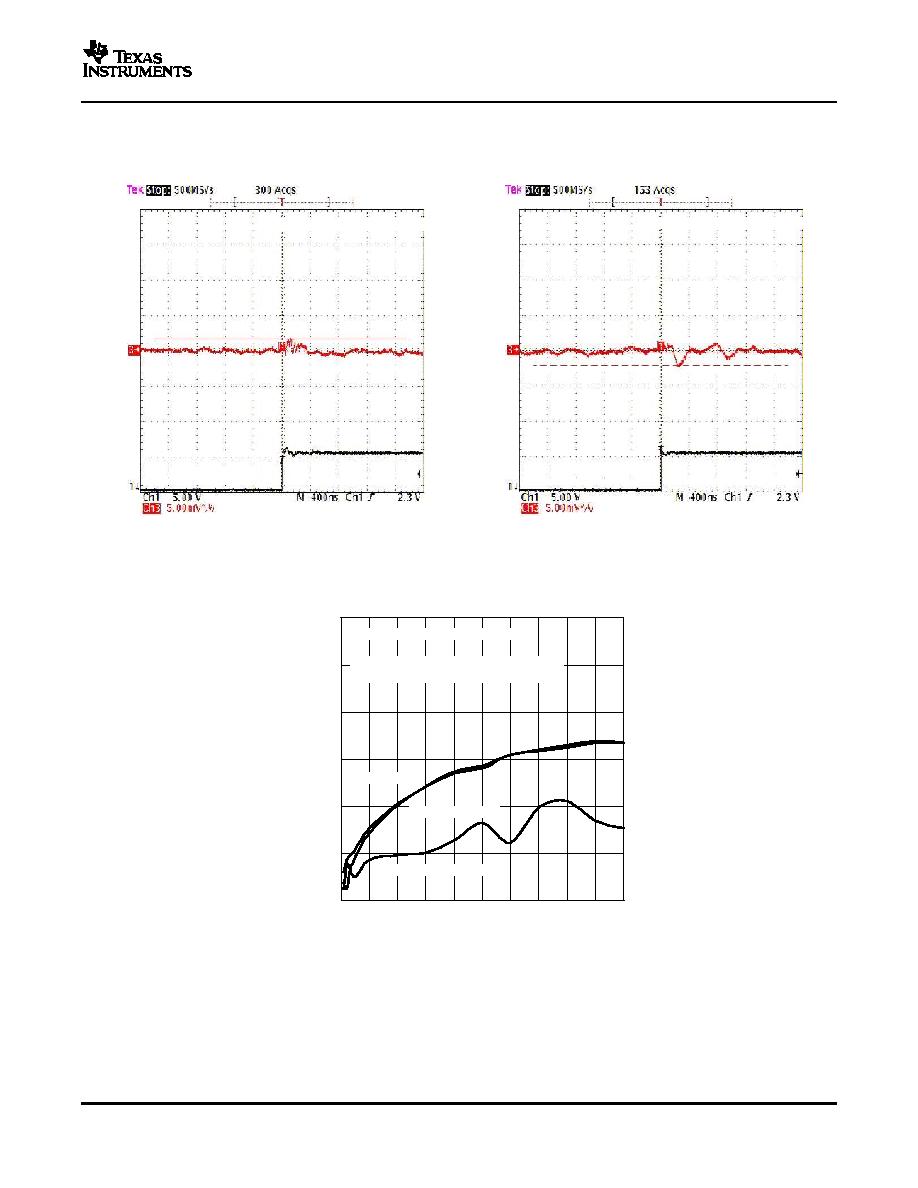
TYPICAL CHARACTERISTICS (continued)
HISTOGRAM OF CURRENT CONSUMPTION - 2.7 V
TOTAL ERROR - 5 V
Figure 32.
Figure 33.
TOTAL ERROR - 2.7 V
EXITING POWER-DOWN MODE
Figure 34.
Figure 35.
15

www.ti.com
0
1
2
3
4
5
V
DD
= 5 V,
Output Loaded
With 200 pF to GND,
Code 41 to 4055
- Output V
oltage - V
V
O
t - Time - 5
m
s/div
0
1
2
3
V
DD
= 2.5 V,
Output Loaded
With 200 pF to GND,
Code 41 to 4055
- Output V
oltage - V
V
O
t - Time - 5
m
s/div
Trigger Pulse
t - Time - 400 nS/div
- Output V
oltage
V
O
V
DD
= 5 V, V
REF
= 4.096 V
Trigger Pulse
t - Time - 400 nS/div
- Output V
oltage
V
O
V
DD
= 5 V, V
REF
= 4.096 V
DAC7558
SLAS435 ≠ MAY 2005
TYPICAL CHARACTERISTICS (continued)
LARGE-SIGNAL SETTLING TIME - 5 V
LARGE-SIGNAL SETTLING TIME - 2.7 V
Figure 36.
Figure 37.
MIDSCALE GLITCH
WORST-CASE GLITCH
Figure 38.
Figure 39.
16
www.ti.com
Trigger Pulse
t - Time - 400 nS/div
- Output V
oltage
V
O
V
DD
= 5 V, V
REF
= 4.096 V
Trigger Pulse
t - Time - 400 nS/div
- Output V
oltage
V
O
V
DD
= 5 V, V
REF
= 4.096 V
-100
-90
-80
-70
-60
-50
-40
0
1
2
3
4
5
6
7
8
9
10
THD
2nd Harmonic
3rd Harmonic
T
otal Harmonic Distortion - dB
Output Frequency - kHz
V
DD
= 5 V, V
REF
= 4.096 V
- 1dB FSR Digital Input, Fs = 1 Msps
Measurement Bandwidth = 20 kHz
DAC7558
SLAS435 ≠ MAY 2005
TYPICAL CHARACTERISTICS (continued)
CHANNEL-TO-CHANNEL CROSSTALK
DIGITAL FEEDTHROUGH ERROR
FOR A FULL-SCALE SWING
Figure 40.
Figure 41.
TOTAL HARMONIC DISTORTION
vs
OUTPUT FREQUENCY
Figure 42.
17
www.ti.com
3-Wire Serial Interface
DAC7558
SLAS435 ≠ MAY 2005
The DAC7558 digital interface is a standard 3-wire SPI/QSPI/Microwire/DSP-compatible interface.
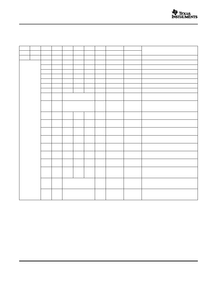
Table 1. Serial Interface Programming
DB23
DB22
DB21
DB20
DB19
DB18
DB17
DB16
DB15≠DB4
DB3≠DB0
DESCRIPTION
A1
A0
LD1
LD0
SEL2
SEL1
SEL0
PWD
MSB≠LSB
Don't Care
0
0
0
0
0
0
0
0
Data
X
Write to buffer A with data
0
0
0
0
1
0
Data
X
Write to buffer B with data
0
0
0
1
0
0
Data
X
Write to buffer C with data
0
0
0
1
1
0
Data
X
Write to buffer D with data
0
0
1
0
0
0
Data
X
Write to buffer E with data
0
0
1
0
1
0
Data
X
Write to buffer F with data
0
0
1
1
0
0
Data
X
Write to buffer G with data
0
0
1
1
1
0
Data
X
Write to buffer H with data
0
1
(000, 001, 010, 011,
0
Data
X
Write to buffer with data and load DAC
100, 101, 110, 111)
(selected by DB19, DB18, and DB17)
1
0
(000, 001, 010, 011,
0
Data
X
Write to buffer with data and load DAC
100, 101, 110, 111)
(selected by DB19, DB18, and DB17) and
load all other DACs with buffer data
1
1
0
0
0
0
Data
X
Load DACs A and B with current buffer
(Both A1 and
data
A0 should be
1
1
0
0
1
0
Data
X
Load DACs A, B, C, and D with current
set to zero for
buffer data
normal device
1
1
0
1
0
0
Data
X
Load DACs A, B, C, D, E, and F with
operation.
current buffer data
DAC(s) do not
respond if any
1
1
0
1
1
0
Data
X
Load DACs A, B, C, D, E, F, G, and H
other combi-
with current buffer data
nation is used)
1
1
1
0
0
0
Data
X
Write to buffer with new data and load
DACs A and B simultaneously
1
1
1
0
1
0
Data
X
Write to buffer with new data and load
DACs A, B, C, and D simultaneously
1
1
1
1
0
0
Data
X
Write to buffer with new data and load
DACs A, B, C, D, E, and F simultaneously
1
1
1
1
1
0
Data
X
Write to buffer with new data and load
DACs A, B, C, D, E, F, G, and H
simultaneously
Write to buffer and load DAC with
(000, 001, 010, 011,
X
0
1
See
Table 2
X
Power-Down command to individual chan-
100, 101, 110, 111)
nel (selected by DB19, DB18, and DB17)
X
Write to buffer and load DACs with
(000, 001, 010, 011,
See
Table 2
X
1
1
Power-Down command to multiple chan-
100, 101, 110, 111)
and
Table 3
nels (selected by DB19, DB18, and DB17)
18
www.ti.com
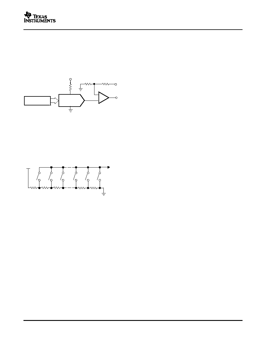
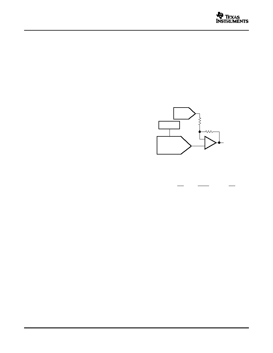
THEORY OF OPERATION
D/A SECTION
OUTPUT BUFFER AMPLIFIERS
DAC External Reference Input
_
+
Resistor String
Ref +
Ref -
DAC Register
V
OUT
V
REF
GND
V
FB
100 k
W
100 k
W
50 k
W
Amplifier Sense Input
V
REF
To Output
Amplifier
R
R
R
R
GND
RESISTOR STRING
Power-On Reset
DAC7558
SLAS435 ≠ MAY 2005
The architecture of the DAC7558 consists of a string
The output buffer amplifier is capable of generating
DAC followed by an output buffer amplifier.
Figure 43
rail-to-rail voltages on its output, which gives an
shows a generalized block diagram of the DAC
output range of 0 V to V
DD
. It is capable of driving a
architecture.
load of 2 k
in parallel with up to 1000 pF to GND.
The source and sink capabilities of the output ampli-
fier can be seen in the typical curves. The slew rate is
1 V/µs with a half-scale settling time of 3 µs with the
output unloaded.
Four separate reference pins are provided for eight
DACs, providing maximum flexibility. VREF1 serves
DAC A and DAC B, VREF2 serves DAC C and DAC
Figure 43. Typical DAC Architecture
D, VREF3 serves DAC E and DAC F, and VREF4
serves DAC G and DAC H. VREF1 through VREF4
can be externally shorted together for simplicity.
The input coding to the DAC7558 is unsigned binary,
which gives the ideal output voltage as:
It is recommended to use a buffered reference in the
V
OUT
= V
REF
◊ D/4096
external circuit (e.g., REF3140). The input impedance
is typically 50 k
for each reference input pin.
Where D = decimal equivalent of the binary code that
is loaded to the DAC register which can range from 0
to 4095.
The DAC7558 contains eight amplifier feedback input
pins, VFBA ... VFBH. For voltage output operation,
VFBA ... VFBH must externally connect to VOUTA ...
VOUTH respectively. For better DC accuracy, these
connections should be made at load points. The
VFBA ... VFBH pins are also useful for a variety of
applications, including
digitally
controlled
current
sources. Each feedback input pin is internally connec-
ted to the DAC amplifier's negative input terminal
Figure 44. Typical Resistor String
through a 100-k
resistor; and, the amplifier's nega-
tive input terminal internally connects to ground
through another 100-k
resistor (See
Figure 43
). This
forms a gain-of-two, non-inverting amplifier configur-
The resistor string section is shown in
Figure 44
. It is
ation. Overall gain remains one because the resistor
simply a string of resistors, each of value R. The
string has a divide-by-two configuration. The resist-
DAC7558 uses eight separate resistor strings. Each
ance seen at each VFBx pin is approximately 200 k
VREFx input pin provides the external reference
to ground.
voltage for two resistor strings. A resistor string has
100 k
total resistance to ground, including a 50 k
divide-by-two resistor. Since each VREFx pin con-
On power up, all internal registers are cleared and all
nects to two resistor strings, the resistance seen by
channels are updated with zero-scale voltages. Until
each VREFx pin is approximately 50 k
. The div-
valid data is written, all DAC outputs remain in this
ide-by-two function provided by the resistor string is
state. This is particularly useful in applications where
compensated by a gain-of-two amplifier configuration.
it is important to know the state of the DAC outputs
The voltage is tapped off by closing one of the
while the device is powering up. In order not to turn
switches connecting the string to the amplifier. Be-
on ESD protection devices, V
DD
should be applied
cause it is a string of resistors, it is specified
before any other pin is brought high.
monotonic. The DAC7558 architecture uses eight
separate
resistor
strings
to
minimize
chan-
During power up, all digital input pins should be set at
nel-to-channel crosstalk.
logic-low voltages. Shortly after power up, if RSTSEL
pin is low, then all DAC outputs are at their
zero-scale voltages. If RSTSEL pin is brought high,
then all DAC outputs are at their mid-scale voltages.
19
www.ti.com
Power Down
Input Data Format Selection
SERIAL INTERFACE
24-Bit Word and Input Shift Register
Asynchronous Clear
DAC7558
SLAS435 ≠ MAY 2005
brought low. The RST signal resets all internal
registers, and therefore behaves like the Power-On
The DAC7558 has a flexible power-down capability
Reset. The DAC7558 updates at the first rising edge
as described in
Table 2
and
Table 3
. Individual
of the SYNC signal that occurs after the RST pin is
channels can be powered down separately, or mul-
brought back to high.
tiple channels can be powered down simultaneously.
During a power-down condition, the user has flexi-
If the RSTSEL pin is high, RST signal going low
bility to select the output impedance of each channel.
resets all outputs to midscale. If the RSTSEL pin is
If the PD pin is brought low, then all channels can
low, RST signal going low resets all outputs to
simultaneously be powered down, with the output at
zero-scale.
high impedance state (High-Z).
The DAC7558 has DB16 as a power-down flag. If this
flag is set, then DB11 and DB10 select one of the
DAC7558 can use unsigned binary (USB) or binary
three power-down modes of the device as described
twos complement (BTC) input data formats. Format
in
Table 2
.
selection is done by the RSTSEL pin. If the RSTSEL
is kept low, the 12-bit input data is assumed to have
Table 2. DAC7558 Power-Down Modes
USB format, and any asynchronous clear operation
generates zero-scale outputs. If the RSTSEL pin is
DB11
DB10
OPERATING MODE
kept high, the 12-bit input data is assumed to have
0
0
PWD Hi-Z
BTC format and any asynchronous clear operation
0
1
PWD 1 k
generates mid-scale outputs.
1
0
PWD 100 k
1
1
PWD Hi-Z
The DAC7558 is controlled over a versatile 3-wire
The DAC7558 can also be powered down using the
serial interface, which operates at clock rates up to
PD pin. When the PD pins is brought low, all
50 MHz and is compatible with SPI, QSPI, Microwire,
channels simultaneously power down and all outputs
and DSP interface standards.
become high impedance. When the PD pin is brought
high, the device resumes its state before the power
down condition.
The input shift register is 24 bits wide. DAC data is
The DAC7558 also has an option to power down
loaded into the device as a 24-bit word under the
individual channels, or multiple channels simul-
control of a serial clock input, SCLK, as shown in the
taneously selected by DB20. If DB20 = 0, then the
Figure 1
timing diagram. The 24-bit word, illustrated
user can power down the selected individual chan-
in
Table 1
, consists of 8 control bits, followed by 12
nels. If DB20 = 1, then the user can power down the
data bits and 4 don't care bits. Data format is straight
multiple channels simultaneously as explained in
binary (RSTSEL pin = 0) or binary twos complement
Table 3
. Power-down mode is selected by DB11 and
(RSTSEL = 1), where the most significant DAC data
DB10.
bit is DB15. Data is loaded MSB first (DB23) where
the first two bits (DB23 and DB22) should be set to
Table 3. DAC7558 Power-Down Modes for Multiple
zero for DAC7558 to work. The DAC7558 does not
Channels
respond to any other combination other than 00.
DB19
DB18
DB17
OPERATING MODE
DB21 and DB20 (LD1 and LD0) determine if the input
0
0
0
PWD Channel A-B
register, DAC register, or both are updated with shift
register input data. DB19, DB18, and DB17 (SEL2,
0
0
1
PWD Channel A-C
SEL1, and SEL0) bits select the desired DAC(s).
0
1
0
PWD Channel A-D
DB16 is the power-down bit. If DB16 = 0, then it is a
0
1
1
PWD Channel A-E
normal operation, if DB16 = 1, then DB11 and DB10
1
0
0
PWD Channel A-F
determine the power-down mode (Hi-Z, 1 k
, or 100
1
0
1
PWD Channel A-G
k
). DB20 bit also gives the user the option of
powering down either a single channel or multiple
1
1
0
PWD Channel A-H
channels at the same time. See Power Down section
1
1
1
PWD Channel A-H
for more details.
The SYNC input is a level-triggered input that acts as
a frame-synchronization signal and chip enable. Data
The DAC7558 output is asynchronously set to
can only be transferred into the device while SYNC is
zero-scale voltage immediately after the RST pin is
low. To start the serial data transfer, SYNC should be
taken low, observing the minimum SYNC-to-SCLK
20
www.ti.com
IOVDD and Level Shifters
INTEGRAL AND DIFFERENTIAL LINEARITY
GLITCH ENERGY
Daisy-Chain Operation
CHANNEL-TO-CHANNEL CROSSTALK
DAC7558
SLAS435 ≠ MAY 2005
falling-edge setup time, t4. After SYNC goes low,
edges are received (following a falling SYNC), the
serial data is shifted into the device's input shift
data stream becomes complete, and SYNC can be
register on the falling edges of SCLK for 24 clock
brought high to update n devices simultaneously.
pulses.
Any
data
and
clock
pulses
after
the
SDO operation is specified at a maximum SCLK
twenty-fourth falling edge of SCLK are ignored. No
speed of 10 MHz.
further serial data transfer occurs until SYNC is taken
Daisy-chain operation is also possible between
high and low again.
octal-channel DAC7558, dual-channel DAC7552, and
SYNC may be taken high after the falling edge of the
single-channel DAC7551 devices. Dasy chaining en-
twenty-fourth SCLK pulse, observing the minimum
ables communication with any number of DAC chan-
SCLK Loop falling-edge to SYNC rising-edge time, t7.
nels using a single serial interface. As long as the
correct number of bits are shifted using a daisy-chain
After the end of serial data transfer, data is automati-
setting, a rising edge of SYNC properly updates all
cally transferred from the input shift register to the
chips in the system. Following a rising edge of SYNC,
input register of the selected DAC. If SYNC is taken
all devices on the daisy chain respond according to
high before the twenty-fourth falling edge of SCLK,
the control bits they receive.
the data transfer is aborted and the DAC input
registers are not updated.
When DCEN is low, the SDO pin is brought to a Hi-Z
The DAC7558 can be used with different logic famil-
state. The first 24 data bits that follow the falling edge
ies that require a wide range of supply voltages (from
of SYNC are stored in the shift register. The rising
1.8 V to 5.5 V). To enable this useful feature, the
edge of SYNC that follows the 24th data bit updates
IOVDD pin must be connected to the logic supply
the DAC(s). If SYNC is brought high before the 24th
voltage of the system. All DAC7558 digital input and
data bit, no action occurs.
output pins are equipped with level-shifter circuits.
Level shifters at the input pins ensure that external
In daisy-chain mode (DCEN = 1) the DAC7558
logic high voltages are translated to the internal logic
requires a falling SCLK edge after the rising SYNC, in
high voltage, with no additional power dissipation.
order to initialize the serial interface for the next
Similarly, the level shifter for the SDO pin translates
update.
the internal logic high voltage (AVDD) to the external
When DCEN is high, data can continuously be shifted
logic high level (IOVDD). For single supply operation,
into the shift register, enabling the daisy-chain oper-
the IOVDD pin can be tied to the AVDD pin.
ation. The SDO pin becomes active and outputs
SDIN data with 24 clock-cycle delay. A rising edge of
SYNC loads the shift register data into the DAC(s).
The loaded data consists of the last 24 data bits
The DAC7558 uses precision thin-film resistors pro-
received into the shift register before the rising edge
viding exceptional linearity and monotonicity. Integral
of SYNC.
linearity error is typically within (+/-) 0.35 LSBs, and
differential linearity error is typically within (+/-) 0.08
If daisy-chain operation is not needed, DCEN should
LSBs.
permanently be tied to a logic-low voltage.
The DAC7558 uses a proprietary architecture that
When the DCEN pin is brought high, daisy chaining is
minimizes glitch energy. The code-to-code glitches
enabled. Serial data output (SDO) pin is provided to
are so low, they are usually buried within the
daisy-chain multiple DAC7558 devices in a system.
wide-band noise and cannot be easily detected. The
As long as SYNC is high or DCEN is low the SDO pin
DAC7558 glitch is typically well under 0.1 nV-s. Such
is in a high-impedance state. When SYNC is brought
low glitch energy provides more than 10X improve-
low the output of the internal shift register is tied to
ment over industry alternatives.
the SDO pin. As long as SYNC is low and DCEN is
high, SDO duplicates the SDIN signal with 24-cycle
delay. To support multiple devices in a daisy-chain,
SCLK and SYNC signals are shared across all
The DAC7558 architecture is designed to minimize
devices and SDO of one DAC7558 should be tied to
channel-to-channel crosstalk. The voltage change in
the SDIN of the next DAC7558. For n devices in such
one channel does not affect the voltage output in
a daisy chain, 24n SCLK cycles are required to shift
another channel. The DC crosstalk is in the order of a
the entire input data stream. After 24n SCLK falling
few microvolts. AC crosstalk is also less than ≠100
dBs. This provides orders of magnitude improvement
over certain competing architectures.
21
www.ti.com
APPLICATION INFORMATION
Waveform Generation
Generating ±5-V, ±10-V, and ± 12-V Outputs For
DAC7558
REFIN
DAC7558
_
+
V
dac
R2
R1
REF3140
V
ref
V
tail
V
OUT
OPA4130
V
OUT
+
V
REF
R2
R1
)
1
Din
4096
*
V
tail
R2
R1
(1)
DAC7558
SLAS435 ≠ MAY 2005
glitches can also slow the loop down. With its 1
MSPS (small-signal) maximum data update rate,
DAC7558 can support high-speed control loops.
Ultra-low glitch energy of the DAC7558 significantly
Due to its exceptional linearity, low glitch, and low
improves loop stability and loop settling time.
crosstalk, the DAC7558 is well suited for waveform
generation (from DC to 10 kHz). The DAC7558
Generating Industrial Voltage Ranges:
large-signal settling time is 5 µs, supporting an
For control loop applications, DAC gain and offset
update rate of 200 KSPS. However, the update rates
errors are not important parameters. This could be
can exceed 1 MSPS if the waveform to be generated
exploited to lower trim and calibration costs in a
consists of small voltage steps between consecutive
high-voltage control circuit design. Using a quad
DAC updates. To obtain a high dynamic range,
operational amplifier (OPA4130), and a voltage refer-
REF3140 (4.096 V) or REF02 (5.0 V) are rec-
ence (REF3140), the DAC7558 can generate the
ommended for reference voltage generation.
wide voltage swings required by the control loop.
Precision Industrial Control
Industrial control applications can require multiple
feedback loops consisting of sensors, ADCs, MCUs,
DACs, and actuators. Loop accuracy and loop speed
are the two important parameters of such control
loops.
Loop Accuracy:
In a control loop, the ADC has to be accurate. Offset,
gain, and the integral linearity errors of the DAC are
Figure 45. Low-cost, Wide-swing Voltage Gener-
not factors in determining the accuracy of the loop.
ator for Control Loop Applications
As long as a voltage exists in the transfer curve of a
monotonic DAC, the loop can find it and settle to it.
The output voltage of the configuration is given by:
On the other hand, DAC resolution and differential
linearity do determine the loop accuracy, because
each DAC step determines the minimum incremental
change the loop can generate. A DNL error less than
Fixed R1 and R2 resistors can be used to coarsely
≠1 LSB (non-monotonicity) can create loop instability.
set the gain required in the first term of the equation.
A DNL error greater than +1 LSB implies unnecess-
Once R2 and R1 set the gain to include some
arily large voltage steps and missed voltage targets.
minimal over-range, four DAC7558 channels could be
With high DNL errors, the loop looses its stability,
used to precisely set the required offset voltages.
resolution, and accuracy. Offering 12-bit ensured
Residual errors are not an issue for loop accuracy
monotonicity and ± 0.08 LSB typical DNL error, 755X
because offset and gain errors could be tolerated.
DACs are great choices for precision control loops.
Four DAC7558 channels can provide the V
tai
l volt-
Loop Speed:
ages to minimize offset error, while the other four
DAC7558 channels provide Vdac voltages to gener-
Many factors determine control loop speed. Typically,
ate four high-voltage outputs.
the ADC's conversion time, and the MCU's compu-
tation time are the two major factors that dominate
For ±5-V operation: R1=10 k
, R2 = 15 k
, V
tail
=
the time constant of the loop. DAC settling time is
3.33 V, V
REF
= 4.096 V
rarely a dominant factor because ADC conversion
For ±10-V operation: R1=10 k
, R2 = 39 k
, V
tail
=
times usually exceed DAC conversion times. DAC
2.56 V, V
REF
= 4.096 V
offset, gain, and linearity errors can slow the loop
down only during the start-up. Once the loop reaches
For ±12-V operation: R1=10 k
, R2 = 49 k
, V
tail
=
its steady-state operation, these errors do not affect
2.45 V, V
REF
= 4.096 V
loop speed any further. Depending on the ringing
characteristics of the loop's transfer function, DAC
22

PACKAGING INFORMATION
Orderable Device
Status
(1)
Package
Type
Package
Drawing
Pins Package
Qty
Eco Plan
(2)
Lead/Ball Finish
MSL Peak Temp
(3)
DAC7558IRHBR
ACTIVE
QFN
RHB
32
3000
TBD
CU NIPDAU
Level-2-235C-1 YEAR
DAC7558IRHBT
ACTIVE
QFN
RHB
32
250
TBD
CU NIPDAU
Level-2-235C-1 YEAR
(1)
The marketing status values are defined as follows:
ACTIVE: Product device recommended for new designs.
LIFEBUY: TI has announced that the device will be discontinued, and a lifetime-buy period is in effect.
NRND: Not recommended for new designs. Device is in production to support existing customers, but TI does not recommend using this part in
a new design.
PREVIEW: Device has been announced but is not in production. Samples may or may not be available.
OBSOLETE: TI has discontinued the production of the device.
(2)
Eco
Plan
-
The
planned
eco-friendly
classification:
Pb-Free
(RoHS)
or
Green
(RoHS
&
no
Sb/Br)
-
please
check
http://www.ti.com/productcontent
for the latest availability information and additional product content details.
TBD: The Pb-Free/Green conversion plan has not been defined.
Pb-Free (RoHS): TI's terms "Lead-Free" or "Pb-Free" mean semiconductor products that are compatible with the current RoHS requirements
for all 6 substances, including the requirement that lead not exceed 0.1% by weight in homogeneous materials. Where designed to be soldered
at high temperatures, TI Pb-Free products are suitable for use in specified lead-free processes.
Green (RoHS & no Sb/Br): TI defines "Green" to mean Pb-Free (RoHS compatible), and free of Bromine (Br) and Antimony (Sb) based flame
retardants (Br or Sb do not exceed 0.1% by weight in homogeneous material)
(3)
MSL, Peak Temp. -- The Moisture Sensitivity Level rating according to the JEDEC industry standard classifications, and peak solder
temperature.
Important Information and Disclaimer:The information provided on this page represents TI's knowledge and belief as of the date that it is
provided. TI bases its knowledge and belief on information provided by third parties, and makes no representation or warranty as to the
accuracy of such information. Efforts are underway to better integrate information from third parties. TI has taken and continues to take
reasonable steps to provide representative and accurate information but may not have conducted destructive testing or chemical analysis on
incoming materials and chemicals. TI and TI suppliers consider certain information to be proprietary, and thus CAS numbers and other limited
information may not be available for release.
In no event shall TI's liability arising out of such information exceed the total purchase price of the TI part(s) at issue in this document sold by TI
to Customer on an annual basis.
PACKAGE OPTION ADDENDUM
www.ti.com
19-May-2005
Addendum-Page 1

IMPORTANT NOTICE
Texas Instruments Incorporated and its subsidiaries (TI) reserve the right to make corrections, modifications,
enhancements, improvements, and other changes to its products and services at any time and to discontinue
any product or service without notice. Customers should obtain the latest relevant information before placing
orders and should verify that such information is current and complete. All products are sold subject to TI's terms
and conditions of sale supplied at the time of order acknowledgment.
TI warrants performance of its hardware products to the specifications applicable at the time of sale in
accordance with TI's standard warranty. Testing and other quality control techniques are used to the extent TI
deems necessary to support this warranty. Except where mandated by government requirements, testing of all
parameters of each product is not necessarily performed.
TI assumes no liability for applications assistance or customer product design. Customers are responsible for
their products and applications using TI components. To minimize the risks associated with customer products
and applications, customers should provide adequate design and operating safeguards.
TI does not warrant or represent that any license, either express or implied, is granted under any TI patent right,
copyright, mask work right, or other TI intellectual property right relating to any combination, machine, or process
in which TI products or services are used. Information published by TI regarding third-party products or services
does not constitute a license from TI to use such products or services or a warranty or endorsement thereof.
Use of such information may require a license from a third party under the patents or other intellectual property
of the third party, or a license from TI under the patents or other intellectual property of TI.
Reproduction of information in TI data books or data sheets is permissible only if reproduction is without
alteration and is accompanied by all associated warranties, conditions, limitations, and notices. Reproduction
of this information with alteration is an unfair and deceptive business practice. TI is not responsible or liable for
such altered documentation.
Resale of TI products or services with statements different from or beyond the parameters stated by TI for that
product or service voids all express and any implied warranties for the associated TI product or service and
is an unfair and deceptive business practice. TI is not responsible or liable for any such statements.
Following are URLs where you can obtain information on other Texas Instruments products and application
solutions:
Products
Applications
Amplifiers
amplifier.ti.com
Audio
www.ti.com/audio
Data Converters
dataconverter.ti.com
Automotive
www.ti.com/automotive
DSP
dsp.ti.com
Broadband
www.ti.com/broadband
Interface
interface.ti.com
Digital Control
www.ti.com/digitalcontrol
Logic
logic.ti.com
Military
www.ti.com/military
Power Mgmt
power.ti.com
Optical Networking
www.ti.com/opticalnetwork
Microcontrollers
microcontroller.ti.com
Security
www.ti.com/security
Telephony
www.ti.com/telephony
Video & Imaging
www.ti.com/video
Wireless
www.ti.com/wireless
Mailing Address:
Texas Instruments
Post Office Box 655303 Dallas, Texas 75265
Copyright
2005, Texas Instruments Incorporated