
D A C
7 5 1
2
www.ti.com
FEATURES
DESCRIPTION
APPLICATIONS
V
DD
SCL
A0
GND
Output
Buffer
Power Down
Control Logic
Resistor
Network
Ref (+) REF(-)
12-Bit
DAC
I
2
C
Control
Logic
DAC
Register
Power-On
Reset
V
OUT
SDA
DAC7571
SLAS374A ≠ FEBRUARY 2003 ≠ REVISED JANUARY 2004
+2.7 V to +5.5 V, I
2
C INTERFACE, VOLTAGE OUTPUT, 12-BIT DIGITAL-TO-ANALOG
CONVERTER
∑
Micropower Operation: 140 µA @ 5 V
The DAC7571 is a low-power, single channel, 12-bit
∑
Power-On Reset to Zero
buffered voltage output DAC. Its on-chip precision
output amplifier allows rail-to-rail output swing to be
∑
+2.7-V to +5.5 V-Power Supply
achieved. The DAC7571 utilizes an I
2
C compatible
∑
Specified Monotonic by Design
two wire serial interface that operates at clock rates
∑
Settling Time: 10 µs to
±
0.003%FS
up to 3.4 Mbps with address support of up to two
∑
I
2
CTM Interface up to 3.4 Mbps
DAC7571s on the same data bus.
∑
On-Chip Output Buffer Amplifier, Rail-to-Rail
The output voltage range of the DAC is set to V
DD
.
Operation
The DAC7571 incorporates a power-on-reset circuit
∑
Double-Buffered Input Register
that ensures that the DAC output powers up at zero
∑
Address Support for up to Two DAC7571s
volts and remains there until a valid write to the
device
takes
place.
The
DAC7571
contains
a
∑
Small 6 Lead SOT Package
power-down feature, accessed via the internal control
∑
Operation From ≠40
∞
C to 105
∞
C
register, that reduces the current consumption of the
device to 50 nA at 5 V.
The low power consumption of this part in normal
∑
Process Control
operation makes it ideally suited for portable battery
∑
Data Acquistion Systems
operated equipment. The power consumption is less
∑
Closed-Loop Servo Control
than 0.7 mW at V
DD
= 5 V reducing to 1 µW in
∑
PC Peripherals
power-down mode.
∑
Portable Instrumentation
The DAC7571 is available in a 6-lead SOT 23
package.
Please be aware that an important notice concerning availability, standard warranty, and use in critical applications of Texas
Instruments semiconductor products and disclaimers thereto appears at the end of this data sheet.
I
2
C is a trademark of Philips Corporation.
PRODUCTION DATA information is current as of publication date.
Copyright © 2003≠2004, Texas Instruments Incorporated
Products conform to specifications per the terms of the Texas
Instruments standard warranty. Production processing does not
necessarily include testing of all parameters.

www.ti.com
PIN CONFIGURATIONS
A0
SCL
SDA
6
5
4
1
2
3
V
OUT
GND
V
DD
D771
1
2
3
6
5
4
YMLL
(TOP VIEW)
(BOTTOM VIEW)
Lot Trace Code
ABSOLUTE MAXIMUM RATINGS
(1)
ELECTRICAL CHARACTERISTICS
DAC7571
SLAS374A ≠ FEBRUARY 2003 ≠ REVISED JANUARY 2004
These devices have limited built-in ESD protection. The leads should be shorted together or the device placed in conductive foam
during storage or handling to prevent electrostatic damage to the MOS gates.
PACKAGE/ORDERING INFORMATION
PACKAGE
SPECIFIED TEM-
PACKAGE
ORDERING NUM-
PRODUCT
PACKAGE
DESIG-
TRANSPORT MEDIA
PERATURE RANGE
MARKING
BER
NATOR
DAC7571IDBVT
250 Piece Small Tape and Reel
DAC7571
SOT23-6
DBV
-40
∞
C to +105
∞
C
D771
DAC7571IDBVR
3000 Piece Tape and Reel
PIN DESCRIPTION (SOT23-6)
PIN
NAME
DESCRIPTION
1
V
OUT
Analog output voltage from DAC
Ground reference point for all
2
GND
circuitry on the part
3
V
DD
Analog Voltage Supply Input
4
SDA
Serial Data Input
5
SCL
Serial Clock Input
6
A0
Device Address Select
LOT
Year (3 = 2003); Month (1≠9 = JAN≠SEP; A=OCT,
TRACE
B=NOV, C=DEC); LL≠ Random code generated
CODE:
when assembly is requested
UNITS
V
DD
to GND
-0.3V to +6V
Digital Input voltage to GND
-0.3 V to +V
DD
+ 0.3 V
V
OUT
to GND
-0.3 V to +V
DD
+ 0.3 V
Operating temperature range
-40
∞
C to + 105
∞
C
Storage temperature range
-65
∞
C to + 150
∞
C
Junction temperature range (T
J
max)
+ 150
∞
C
Power dissipation
(T
J
max - T
A
)R
JA
Thermal impedance, R
JA
240
∞
C/W
Lead temperature, soldering
Vapor phase (60s)
215
∞
C
Infrared (15s)
220
∞
C
(1)
Stresses above those listed under "Absolute Maximum Ratings" may cause permanent damage to the device. Exposure to absolute
maximum conditions for extended periods may affect device reliability.
V
DD
= +2.7 V to +5.5 V; R
L
= 2 k
to GND; C
L
= 200 pF to GND; all specifications -40
∞
C to +105
∞
C unless otherwise noted.
DAC7571
PARAMETER
CONDITIONS
UNITS
MIN
TYP
MAX
STATIC PERFORMANCE
(1)
Resolution
12
Bits
Relative accuracy
±
0.195
% of FSR
Differential nonlinearity
Assured monotonic by design
±
1
LSB
Zero code error
All zeroes loaded to DAC register
5
20
mV
(1)
Linearity calculated using a reduced code range of 48 to 4047; output unloaded.
2

www.ti.com
DAC7571
SLAS374A ≠ FEBRUARY 2003 ≠ REVISED JANUARY 2004
ELECTRICAL CHARACTERISTICS (continued)
V
DD
= +2.7 V to +5.5 V; R
L
= 2 k
to GND; C
L
= 200 pF to GND; all specifications -40
∞
C to +105
∞
C unless otherwise noted.
DAC7571
PARAMETER
CONDITIONS
UNITS
MIN
TYP
MAX
Full-scale error
All ones loaded to DAC register
-0.15
-1.25
% of FSR
Gain error
±
1.25
% of FSR
Zero code error drift
±
7
µV/
∞
C
Gain temperature coefficient
±
3
ppm of FSR/
∞
C
OUTPUT CHARACTERISTICS
(2)
Output voltage range
0
V
DD
V
Output voltage settling time
1/4 Scale to 3/4 scale change (400
H
to C00
H
)
8
10
µ s
Slew rate
1
V/µs
R
L
=
470
pF
Capacitive load stability
R
L
= 2k
1000
pF
Code change glitch impulse
1 LSB Change around major carry
20
nV-s
Digital feedthrough
0.5
nV-s
DC output impedance
1
V
DD
= +5V
50
mA
Short-circuit current
V
DD
= +3V
20
mA
Coming out of power-down mode, V
DD
= +5V
2.5
µ s
Power-up time
Coming out of power-down mode, V
DD
= +3V
5
µ s
LOGIC INPUTS
(3)
Input current
±
1
µ A
V
IN
L, Input low voltage
V
DD
= +3V
0.3
◊
V
DD
V
V
IN
H, Input high voltage
V
DD
= +5V
0.7
◊
V
DD
V
Pin capacitance
3
pF
POWER REQUIREMENTS
V
DD
2.7
5.5
V
I
DD
(normal operation)
DAC active and excluding load current
V
DD
= +3.6V to +5.5V
V
IH
= V
DD
and V
IL
= GND
135
200
µ A
V
DD
= +2.7V to +3.6V
V
IH
= V
DD
and V
IL
= GND
115
160
µ A
I
DD
(all power-down modes)
V
DD
= +3.6 V to +5.5
V
IH
= V
DD
and V
IL
= GND
0.2
1
µ A
V
V
DD
= +2.7V to +3.6V
V
IH
= V
DD
and V
IL
= GND
0.05
1
µ A
POWER EFFICIENCY
I
OUT
/I
DD
I
LOAD
= 2mA, V
DD
= +5V
93
%
(2)
Specified by design and characterization, not production tested.
(3)
Specified by design and characterization, not production tested.
3

www.ti.com
TIMING CHARACTERISTICS
DAC7571
SLAS374A ≠ FEBRUARY 2003 ≠ REVISED JANUARY 2004
SYMBOL
PARAMETER
TEST CONDITIONS
MIN
TYP
MAX
UNITS
Standard mode
100
kHz
Fast mode
400
kHz
f
SCL
SCL Clock Frequency
High-speed mode, C
B
- 100pF max
3.4
MHz
High-Speed mode, C
B
- 400pF max
1.7
MHz
Standard mode
4.7
µs
Bus Free Time Between a STOP
t
BUF
and START Condition
Fast mode
1.3
µs
Standard mode
4.0
µs
Hold Time (Repeated) START
t
HD
; t
STA
Fast mode
600
ns
Condition
High-speed mode
160
ns
Standard mode
4.7
µs
Fast mode
1.3
µs
t
LOW
LOW Period of the SCL Clock
High-speed mode, C
B
- 100pF max
160
ns
High-speed mode, C
B
- 400pF max
320
ns
Standard mode
4.0
µs
Fast mode
600
ns
t
HIGH
HIGH Period of the SCL Clock
High-speed mode, C
B
- 100pF max
60
ns
High-speed mode, C
B
- 400pF max
120
ns
Standard mode
4.7
µs
Setup Time for a Repeated
t
SU
; t
STA
Fast mode
600
ns
START Condition
High-speed mode
160
ns
Standard mode
250
ns
t
SU
; t
DAT
Data Setup Time
Fast mode
100
ns
High-speed mode
10
ns
Standard mode
0
3.45
µs
Fast mode
0
0.9
µs
t
HD
; t
DAT
Data Hold Time
High-speed mode, C
B
- 100pF max
0
70
ns
High-speed mode, C
B
- 400pF max
0
150
ns
Standard mode
1000
ns
Fast mode
20 + 0.1C
B
300
ns
t
RCL
Rise Time of SCL Signal
High-speed mode, C
B
- 100pF max
10
40
ns
High-speed mode, C
B
- 400pF max
20
80
ns
Standard mode
1000
ns
Rise Time of SCL Signal After a
Fast mode
20 + 0.1C
B
300
ns
t
RCL1
Repeated START Condition and
High-speed mode, C
B
- 100pF max
10
80
ns
After an Acknowledge BIT
High-speed mode, C
B
- 400pF max
20
160
ns
Standard mode
300
ns
Fast mode
20 + 0.1C
B
300
ns
t
FCL
Fall Time of SCL Signal
High-speed mode, C
B
- 100pF max
10
40
ns
High-speed mode, C
B
- 400pF max
20
80
ns
Standard mode
1000
ns
Fast mode
20 + 0.1C
B
300
ns
t
RDA
Rise Time of SDA Signal
High-speed mode, C
B
- 100pF max
10
80
ns
High-speed mode, C
B
- 400pF max
20
160
ns
Standard mode
300
ns
Fast mode
20 + 0.1C
B
300
ns
t
FDA
Fall Time of SDA Signal
High-speed mode, C
B
- 100pF max
10
80
ns
High-speed mode, C
B
- 400pF max
20
160
ns
4

www.ti.com
DAC7571
SLAS374A ≠ FEBRUARY 2003 ≠ REVISED JANUARY 2004
TIMING CHARACTERISTICS (continued)
SYMBOL
PARAMETER
TEST CONDITIONS
MIN
TYP
MAX
UNITS
Standard mode
4.0
µs
t
SU
; t
STO
Setup Time for STOP Condition
Fast mode
600
ns
High-speed mode
160
ns
C
B
Capacitive Load for SDA and SCL
400
pF
Fast mode
50
ns
t
SP
Pulse Width of Spike Suppressed
High-speed mode
10
ns
Standard mode
Noise Margin at the HIGH Level
V
NH
for Each Connected Device
Fast mode
0.2V
DD
V
(Including Hysteresis)
High-speed mode
Standard mode
Noise Margin at the LOW Level for
V
NL
Each Connected Device
Fast mode
0.1V
DD
V
(Including Hysteresis)
High-speed mode
5

www.ti.com
TYPICAL CHARACTERISTICS: V
DD
= +5 V
-8
-6
-4
-2
0
2
4
6
8
-1
-0.5
0
0.5
1
0
512
1024
1536
2048
2560
3072
3584
4096
Digital Input Code
LE - LSB
DLE - LSB
-8
-6
-4
-2
0
2
4
6
8
LE - LSB
-1
-0.5
0
0.5
1
0
512
1024
1536
2048
2560
3072
3584
4096
Digital Input Code
DLE - LSB
Digital Input Code
Output Error -mV
-16
-8
0
8
16
0
512
1024
1536
2048
2560
3072
3584 4096
-8
-6
-4
-2
0
2
4
6
8
LE - LSB
DLE - LSB
-1
-0.5
0
0.5
1
0
512
1024
1536
2048
2560
3072
3584
4096
Digital Input Code
-30
-20
-10
0
10
20
30
-50
-30
-10
10
30
50
70
90
110
Zero-Scale Error - mV
T - Temperature -
_
C
-30
-20
-10
0
10
20
30
-50
-30
-10
10
30
50
70
90
110
Zero-Scale Error - mV
T - Temperature -
_
C
DAC7571
SLAS374A ≠ FEBRUARY 2003 ≠ REVISED JANUARY 2004
At T
A
= +25
∞
C, +V
DD
= +5 V, unless otherwise noted.
LINEARITY ERROR AND
LINEARITY ERROR AND
DIFFERENTIAL LINEARITY ERROR
DIFFERENTIAL LINEARITY ERROR
vs
vs
CODE (-40
∞
C)
CODE (+25
∞
C )
Figure 1.
Figure 2.
LINEARITY ERROR AND
DIFFERENTIAL LINEARITY ERROR
vs
CODE (+105
∞
C)
TYPICAL TOTAL UNADJUSTED ERROR
Figure 3.
Figure 4.
ZERO-SCALE ERROR
FULL-SCALE ERROR
vs
vs
TEMPERATURE
TEMPERATURE
Figure 5.
Figure 6.
6
www.ti.com
0
500
1000
1500
2000
2500
80
90
100
1
10
120
130
140
150
160
170
180
190
200
I
DD
- Supply Current -
m
A
f - Frequency - Hz
0
V
O
U
T
(
V
)
I
SOURCE/SINK
(mA)
5
10
15
5
4
3
2
1
0
DAC Loaded with FFF
H
DAC Loaded with 000
H
0
100
200
300
400
500
CODE
000
H
200
H
600
H
A00
H
E00
H
FFF
H
I DD
µ
A
- Supply Current -
0
50
100
150
200
250
300
-50
-30
-10
10
30
50
70
90
110
- Supply Current -
I DD
A
µ
T - Temperature -
_
C
DAC7571
SLAS374A ≠ FEBRUARY 2003 ≠ REVISED JANUARY 2004
TYPICAL CHARACTERISTICS: V
DD
= +5 V (continued)
At T
A
= +25
∞
C, +V
DD
= +5 V, unless otherwise noted.
I
DD
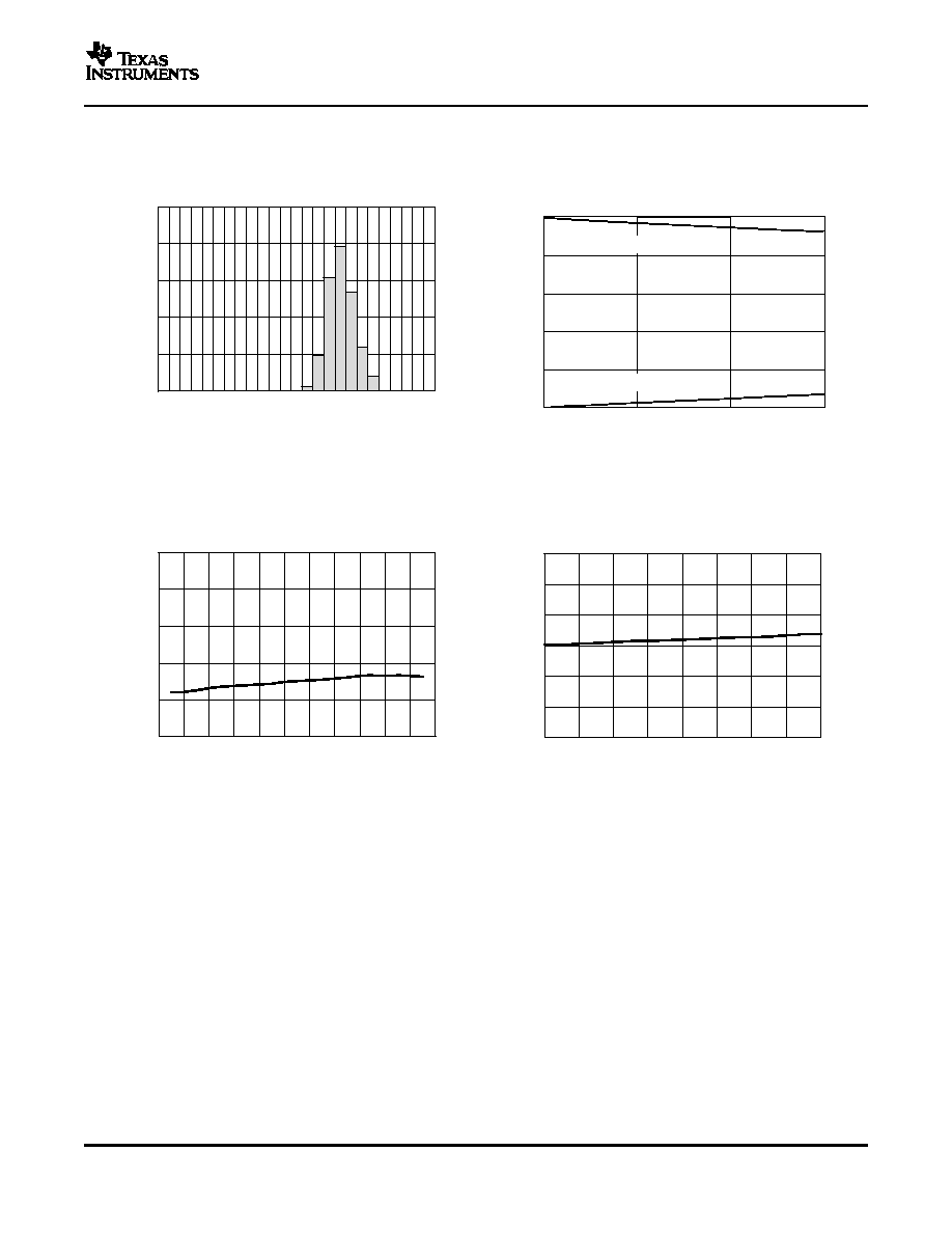
HISTOGRAM
SOURCE AND SINK CURRENT CAPABILITY
Figure 7.
Figure 8.
SUPPLY CURRENT
SUPPLY CURRENT
vs
vs
CODE
TEMPERATURE
Figure 9.
Figure 10.
7

www.ti.com
0
50
100
150
200
250
300
2.7
3.2
3.7
4.2
4.7
5.2
5.7
- Supply Current -
I DD
A
µ
V
DD
- Supply Voltage - V
2.7
I
D
D
(
n
A
)
V
DD
(V)
3.2
3.7
4.2
4.7
5.2
5.7
100
90
80
70
60
50
40
30
20
10
0
+25
∞
C
≠40
∞
C
+105
∞
C
CLK (5V/div)
V
OUT
(1V/div)
Time (1
µ
s/div)
Full-Scale Code Change
000
H
to FFF
H
Output Loaded with
2k
and 200pF to GND
0
I
D
D
(
µ
A
)
V
LOGIC
(V)
1
2
3
4
5
2500
2000
1500
1000
500
0
DAC7571
SLAS374A ≠ FEBRUARY 2003 ≠ REVISED JANUARY 2004
TYPICAL CHARACTERISTICS: V
DD
= +5 V (continued)
At T
A
= +25
∞
C, +V
DD
= +5 V, unless otherwise noted.
SUPPLY CURRENT
POWER-DOWN CURRENT
vs
vs
SUPPLY VOLTAGE
SUPPLY VOLTAGE
Figure 11.
Figure 12.
SUPPLY CURRENT
vs
LOGIC INPUT VOLTAGE
FULL-SCALE SETTLING TIME
Figure 13.
Figure 14.
8

www.ti.com
Time (1
µ
s/div)
CLK (5V/div)
V
OUT
(1V/div)
Full-Scale Code Change
FFF
H
to 000
H
Output Loaded with
2k
and 200pF to GND
HALF-SCALE SETTLING TIME
Time (1
µ
s/div)
CLK (5V/div)
V
OUT
(1V/div)
Half-Scale Code Change
400
H
to C00
H
Output Loaded with
2k
and 200pF to GND
Time (1
µ
s/div)
CLK (5V/div)
V
OUT
(1V/div)
Half-Scale Code Change
C00
H
to 400
H
Output Loaded with
2k
and 200pF to GND
Time (20
µ
s/div)
Loaded with 2k
to V
DD
.
V
DD
(1V/div)
V
OUT
(1V/div)
Time (5
µ
s/div)
CLK (5V/div)
V
OUT
(1V/div)
Time (0.5
µ
s/div)
Loaded with 2k
and 200pF to GND.
Code Change:
800
H
to 7FF
H
.
V
O
U
T
(
2
0
m
V
/
d
i
v
)
DAC7571
SLAS374A ≠ FEBRUARY 2003 ≠ REVISED JANUARY 2004
TYPICAL CHARACTERISTICS: V
DD
= +5 V (continued)
At T
A
= +25
∞
C, +V
DD
= +5 V, unless otherwise noted.
FULL-SCALE SETTLING TIME
HALF-SCALE SETTLING TIME
Figure 15.
Figure 16.
HALF-SCALE SETTLING TIME
POWER-ON RESET TO 0V
Figure 17.
Figure 18.
EXITING POWER-DOWN
(800
H
Loaded)
CODE CHANGE GLITCH
Figure 19.
Figure 20.
9

www.ti.com
TYPICAL CHARACTERISTICS: V
DD
= +2.7V
-8
-6
-4
-2
0
2
4
6
8
-1
-0.5
0
0.5
1
0
512
1024
1536
2048
2560
3072
3584
4096
Digital Input Code
LE - LSB
DLE - LSB
-8
-6
-4
-2
0
2
4
6
8
-1
-0.5
0
0.5
1
0
512
1024
1536
2048
2560
3072
3584
4096
Digital Input Code
LE - LSB
DLE - LSB
-8
-6
-4
-2
0
2
4
6
8
-1
-0.5
0
0.5
1
0
512
1024
1536
2048
2560
3072
3584
4096
Digital Input Code
LE - LSB
DLE - LSB
-16
-8
0
8
16
0
512
1024
1536
2048
2560
3072
3584
Digital Input Code
4096
Output Error - mV
-30
-20
-10
0
10
20
30
-50
-30
-10
10
30
50
70
90
110
Zero-Scale Error - mV
T - Temperature -
_
C
-30
-20
-10
0
10
20
30
-50
-30
-10
10
30
50
70
90
110
T - Temperature -
_
C
Full-Scale Error - mV
DAC7571
SLAS374A ≠ FEBRUARY 2003 ≠ REVISED JANUARY 2004
At T
A
= +25
∞
C, +V
DD
= +2.7V, unless otherwise noted.
LINEARITY ERROR AND
LINEARITY ERROR AND
DIFFERENTIAL LINEARITY ERROR
DIFFERENTIAL LINEARITY ERROR
vs
vs
CODE (-40
∞
C)
CODE (+25
∞
C)
Figure 21.
Figure 22.
LINEARITY ERROR AND
DIFFERENTIAL LINEARITY ERROR
vs
CODE (+105
∞
C)
ABSOLUTE ERROR
Figure 23.
Figure 24.
ZERO-SCALE ERROR
FULL-SCALE ERROR
vs
vs
TEMPERATURE
TEMPERATURE
Figure 25.
Figure 26.
10

www.ti.com
0
500
1000
1500
2000
2500
80
90
100
1
10
120
130
140
150
160
170
180
190
200
I
DD
- Supply Current -
m
A
f - Frequency - Hz
SOURCE AND SINK CURRENT CAPABILITY
0
V
O
U
T
(
V
)
I
SOURCE/SINK
(mA)
5
10
15
3
2
1
0
DAC Loaded with FFF
H
DAC Loaded with 000
H
V
DD
= +3V
0
100
200
300
400
500
000
H
02F
H
200
H
400
H
600
H
800
H
A00
H
C00
H
E00
H
FCF
H
FFF
H
I
DD
- Supply Current -
m
A
f - Frequency - Hz
0
50
100
150
200
250
300
-50
-30
-10
10
30
50
70
90
110
- Supply Current -
I DD
A
µ
T - Temperature -
_
C
FULL-SCALE SETTLING TIME
Time (1
µ
s/div)
CLK (2.7V/div)
V
OUT
(1V/div)
Full-Scale Code Change
000
H
to FFF
H
Output Loaded with
2k
and 200pF to GND
0
I
D
D
(
µ
A
)
V
LOGIC
(V)
1
2
3
4
5
2500
2000
1500
1000
500
0
DAC7571
SLAS374A ≠ FEBRUARY 2003 ≠ REVISED JANUARY 2004
TYPICAL CHARACTERISTICS: V
DD
= +2.7V (continued)
At T
A
= +25
∞
C, +V
DD
= +2.7V, unless otherwise noted.
I
DD
HISTOGRAM
SOURCE AND SINK CURRENT CAPABILITY
Figure 27.
Figure 28.
SUPPLY CURRENT
SUPPLY CURRENT
vs
vs
CODE
9 TEMPERATURE
Figure 29.
Figure 30.
SUPPLY CURRENT
vs
LOGIC INPUT VOLTAGE
FULL SCALE SETTLING TIME
Figure 31.
Figure 32.
11

www.ti.com
FULL-SCALE SETTLING TIME
Time (1
µ
s/div)
CLK (2.7V/div)
V
OUT
(1V/div)
Full-Scale Code Change
FFF
H
to 000
H
Output Loaded with
2k
and 200pF to GND
HALF-SCALE SETTLING TIME
Time (1
µ
s/div)
CLK (2.7V/div)
V
OUT
(1V/div)
Half-Scale Code Change
400
H
to C00
H
Output Loaded with
2k
and 200pF to GND
POWER-ON RESET to 0V
Time (20
µ
s/div)
HALF-SCALE SETTLING TIME
Time (1
µ
s/div)
CLK (2.7V/div)
V
OUT
(1V/div)
Half-Scale Code Change
C00
H
to 400
H
Output Loaded with
2k
and 200pF to GND
H
Time (5
µ
s/div)
CLK (2.7V/div)
V
OUT
(1V/div)
CODE CHANGE GLITCH
Time (0.5
µ
s/div)
Loaded with 2k
and 200pF to GND.
Code Change:
800
H
to 7FF
H
.
V
O
U
T
(
2
0
m
V
/
d
i
v
)
DAC7571
SLAS374A ≠ FEBRUARY 2003 ≠ REVISED JANUARY 2004
TYPICAL CHARACTERISTICS: V
DD
= +2.7V (continued)
At T
A
= +25
∞
C, +V
DD
= +2.7V, unless otherwise noted.
FULL SCALE SETTLING TIME
HALF SCALE SETTLING TIME
Figure 33.
Figure 34.
HALF SCALE SETTLING TIME
POWER ON RESET 0 V
Figure 35.
Figure 36.
EXITING-POWER DOWN (800
H
Loaded)
CODE CHANGE GLITCH
Figure 37.
Figure 38.
12

www.ti.com
THEORY OF OPERATION
D/A SECTION
REF (+)
REF (-)
Resistor
String
Output
Amplifier
V
OUT
GND
V
DD
DAC Register
V
OUT
+
V
DD
D
4096
RESISTOR STRING
R
R
R
R
V
DD
GND
To Output
Amplifier
DAC7571
SLAS374A ≠ FEBRUARY 2003 ≠ REVISED JANUARY 2004
The architecture of the DAC7571 consists of a string DAC followed by an output buffer amplifier. Figure 39
shows a block diagram of the DAC architecture.
Figure 39. R-String DAC Architecture
The input coding to the DAC7571 is unsigned binary, which gives the ideal output voltage as:
where D = decimal equivalent of the binary code that is loaded to the DAC register; it can range from 0 to 4095.
The resistor string section is shown in Figure 40. It is simply a string of resistors, each of value R. The code
loaded into the DAC register determines at which node on the string the voltage is tapped off to be fed into the
output amplifier by closing one of the switches connecting the string to the amplifier. It is ensured monotonic
because it is a string of resistors. The negative tap of the resistor string is tied to GND. The positive tap of the
resistor string is tied to V
DD
.
Figure 40. Resistor String
13

www.ti.com
OUTPUT AMPLIFIER
I
2
C Interface
Start
Condition
SDA
Stop
Condition
SDA
SCL
S
P
SCL
Not Acknowledge
Acknowledge
1
2
8
9
Clock Pulse for
Acknowledgement
S
START
Condition
Data Output
by Transmitter
Data Output
by Receiver
SCL From
Master
DAC7571
SLAS374A ≠ FEBRUARY 2003 ≠ REVISED JANUARY 2004
THEORY OF OPERATION (continued)
The output buffer amplifier is capable of generating rail-to-rail voltages on its output which gives an output range
of 0 V to V
DD
. It is capable of driving a load of 2k
in parallel with 1000 pF to GND. The source and sink
capabilities of the output amplifier can be seen in the typical characteristics. The slew rate is 1V/µs with a
half-scale settling time of 8 µs with the output unloaded.
The DAC7571 uses an I
2
C interface as defined by Philips Semiconductor to receive data in slave mode (see
I
2
C-Bus Specification, Version 2.1, January 2000). The DAC7571 supports the following data transfer modes,
described in the I
2
C-Bus Specification: Standard Mode (100 kbit/s), Fast Mode (400 kbit/s) and High-Speed
Mode (3.4 Mbit/s). Ten-bit addressing and general call addres are not supported.
For simplicity, standard mode and fast mode are referred to as F/S-mode and high-speed mode is referred tg as
HS-mode.
The 2-wire I
2
C serial bus protocol operates as follows:
∑
The Master initiates data transfer by establishing a Start condition. The Start condition is defined when a
high-to-low transition occurs on the SDA line while SCL is high, as shown in Figure 41. The byte following
the start condition is the address byte consisting of the 7-bit slave address followed by the W bit.
Figure 41. START and STOP Conditions
∑
The addressed Slave responds by pulling the SDA pin low during the ninth clock pulse, termed the
Acknowledge bit (see Figure 42). At this stage all other devices on the bus remain idle while the selected
device waits for data to be written to its shift register.
Figure 42. Acknowledge on the I
2
C Bus
∑
Data is transmitted over the serial bus in sequences of nine clock cycles (8 data bits followed by an
acknowledge bit. The transitions on the SDA line must occur during the low period of SCL and remain stable
during the high period of SCL (see Figure 43).
14
www.ti.com
Change of Data Allowed
Data Line
Stable;
Data Valid
SDA
SCL
Recognize START or
REPEATED START
Condition
Recognize STOP or
REPEATED START
Condition
Generate ACKNOWLEDGE
Signal
Acknowledgement
Signal From Slave
SDA
SCL
MSB
P
Sr
Sr
or
P
S
or
Sr
START or
Repeated START
Condition
STOP or
Repeated START
Condition
Clock Line Held Low While
Interrupts are Serviced
1
2
7
8
9
ACK
1
2
3 - 8
9
ACK
Address
R/W
DAC7571
SLAS374A ≠ FEBRUARY 2003 ≠ REVISED JANUARY 2004
THEORY OF OPERATION (continued)
Figure 43. Bit Transfer on the I
2
C Bus
∑
When all data bits have been written, a Stop condition is established (see Figure 44). In writing to the
DAC7571, the master must pull the SDA line high during the tenth clock pulse to establish a Stop condition.
Figure 44. Bus Protocol
15

www.ti.com
SLAVE ADDRESS R/W
A
Ctrl/MS-Byte
A
LS-Byte
A/A
P
"0" (write)
Data Transferred
(n* Words + Acknowledge)
Word = 16 Bit
From Master to DAC7571
From DAC7571 to Master
A = Acknowledge (SDA LOW)
A = Not Acknowledge (SDA HIGH)
S = START Condition
Sr = Repeated START Condition
P = STOP Condition
DAC7571 I
2
C-SLAVE ADDRESS:
1
0
0
1
1
0
A0
R/W
MSB
LSB
Factory Preset
A0 = I
2
C Address Pin
Standard-and Fast-Mode:
S
HS-Master Code
R/W
A
Ctrl/MS-Byte
A
LS-Byte
A/A
P
"0" (write)
Data Transferred
(n* Words + Acknowledge)
Word = 16 Bit
High-Speed-Mode (HS-Mode):
S
A Sr Slave Address
HS-Mode Continues
F/S-Mode
HS-Mode
F/S-Mode
Sr Slave Address
0
0
0
0
1
X
X
R/W
MSB
LSB
HS-Mode Master Code:
0
0
PD1
PD2
D11
D10
D9
D8
MSB
LSB
Ctrl/MS-Byte:
D7
D6
D5
D4
D3
D2
D1
D0
MSB
LSB
LS-Byte:
D11 ≠ D0 = Data Bits
`0' = Write to DAC7571
`1' = Read from DAC7571
ADDRESS BYTE
DAC7571
SLAS374A ≠ FEBRUARY 2003 ≠ REVISED JANUARY 2004
THEORY OF OPERATION (continued)
Figure 45. Master Transmitter Addressing DAC7571 as a Slave Receiver With a 7-Bit Address
MSB
R/W
1
0
0
1
1
0
A0
0
The address byte is the first byte received by the DAC7571 following the START condition from the master
device. The first five bits (MSBs) of the slave address are factory preset to 100110. The next bit of the address
byte is the device select bit, A0. In order for DAC7571 to respond, the logic state of address bit A0 should match
the logic state of address pin A0. A maximum of two devices with the same preset code can therefore be
connected on the same bus at one time. The A0 Address Input can be connected to V
DD
or digital ground, or can
be actively driven by TTL or CMOS logic levels. The device address is set by the state of the A0 pin upon
power-up of the DAC7571. The last bit of the address byte (R/W) should always be zero. Following the START
condition, the DAC7571 monitors the SDA bus, checking the device type identifier being transmitted. Upon
receiving the 100110 code, the appropriate device select bit and the R/W bit, the DAC7571 outputs an
acknowledge signal on the SDA line. Upon receipt of a broadcast address 10010000, the DAC7571 responds
regardless of the state of the A0 pin.
16
www.ti.com
MASTER TRANSMITTER WRITING TO A SLAVE RECEIVER (DAC7571) IN STANDARD/FAST
POWER-ON RESET
POWER-DOWN MODES
DAC7571
SLAS374A ≠ FEBRUARY 2003 ≠ REVISED JANUARY 2004
MODES
I
2
C protocol starts when the bus is dile, that is, when SDA and SCL lines are stable high. The master then pulls
the SDA line low while SCL is still high indicting that serial data transfer has started. This is called a start
condition, and can only be asserted by the master. After the start conditioin, the master generates the serial
clock and puts out an address byte. While generating the bit stream, the master ensures the timing for valid data.
For each valid I
2
C bit, the SDA line should remain stable during the entire high period of the SCL line. The
address byte consists of 7 address bits (1001 100, assuming A0=0) and a direction bit (R/W=0). After sending
the address byte, the master generates a ninth SCL pulse and monitors the state of the SDA line during the high
period of this ninth clock cycle.
The SDA line being pulled low by a receiver during the high period of this 9
th
clock cylce is called an
acknowledge signal. If the master receives an acknowledge signal, it knows that a DAC7571 successfully
matched the address which the master sent. Upon the receipt of this acknowledge, the master knows that the
communication link with a DAC7571 has been established and more data can be sent. The master continues by
sending a Control/MS-byte, which sets DAC7571 operation mode and specifies the first 4 MSBs of data. After
sending the Control/MS-byte, the master expects an acknowledge signal from the DAC7571. Upon the receipt of
the acknowledge, the master sends an LS-byte that represents the 8 least significant bits of DAC7571's 12-bit
conversion data. After receiving the LS-byte, the DAC7571 sends an acknowledge. At the falling edge of the
acknowledge signal, following the LS-byte, the DAC7571 performs a digital to analog conversion. For further
DAC updates, the master can keep repeating Control/MS-byte and LS-byte sequences expecting an
acknowledge after each byte. After the required number of digital to analog conversions is complete, the master
can break the communication link with the DAC7571 by pulling the SDA line from low to high while SCL line is
high. This is called a stop condition . A stop condition brings the bus back to idle (SDA and SCL both high). A
stop condition indicates that communication with the DAC7571 has ended. All devices on the bus, including the
DAC7571, waits for a new start condition followed by a mtaching address byte. DAC7571 stays in a programmed
state until the receipt of a stop condition.
Table 1. Write Sequence in Standard/Fast Modes
Transmitter
MSB
6
5
4
3
2
1
LSB
Comment
Master
Start
Begin Sequence
(1)
Write Addressing (LSB=0, R/W =
Master
1
0
0
1
1
0
A0
0
0)
DAC7571
DAC7571 Acknowledges
Master
0
0
PD1
PD0
D11
D10
D9
D8
Writing Control/MS-Byte
DAC7571
DAC7571 Acknowledges
Master
D7
D6
D5
D4
D3
D2
D1
D0
Writing LS-Byte
DAC7571
DAC7571 Acknowledges
Master
Stop or Repeated Start
(2)
Done
(1)
Once DAC7571 is addressed, high-byte-low-byte sequences can repeat until a stop condition is received.
(2)
Use repeated start to secure bus operation and loop back to the stage of write addressing for next Write.
The DAC7571 contains a power-on reset circuit that controls the output voltage during power-up. On power-up,
the DAC register is filled with zeros and the output voltage is 0 V. It remains at a zero-code output until a valid
write sequence is made to the DAC. This is useful in applications where it is important to know the state of the
DAC output while it is in the process of powering up.
The DAC7571 contains four separate modes of operation. These modes are programmable via two bits (PD1
and PD0). Table 2 shows how the state of these bits correspond to the mode of operation.
17

www.ti.com
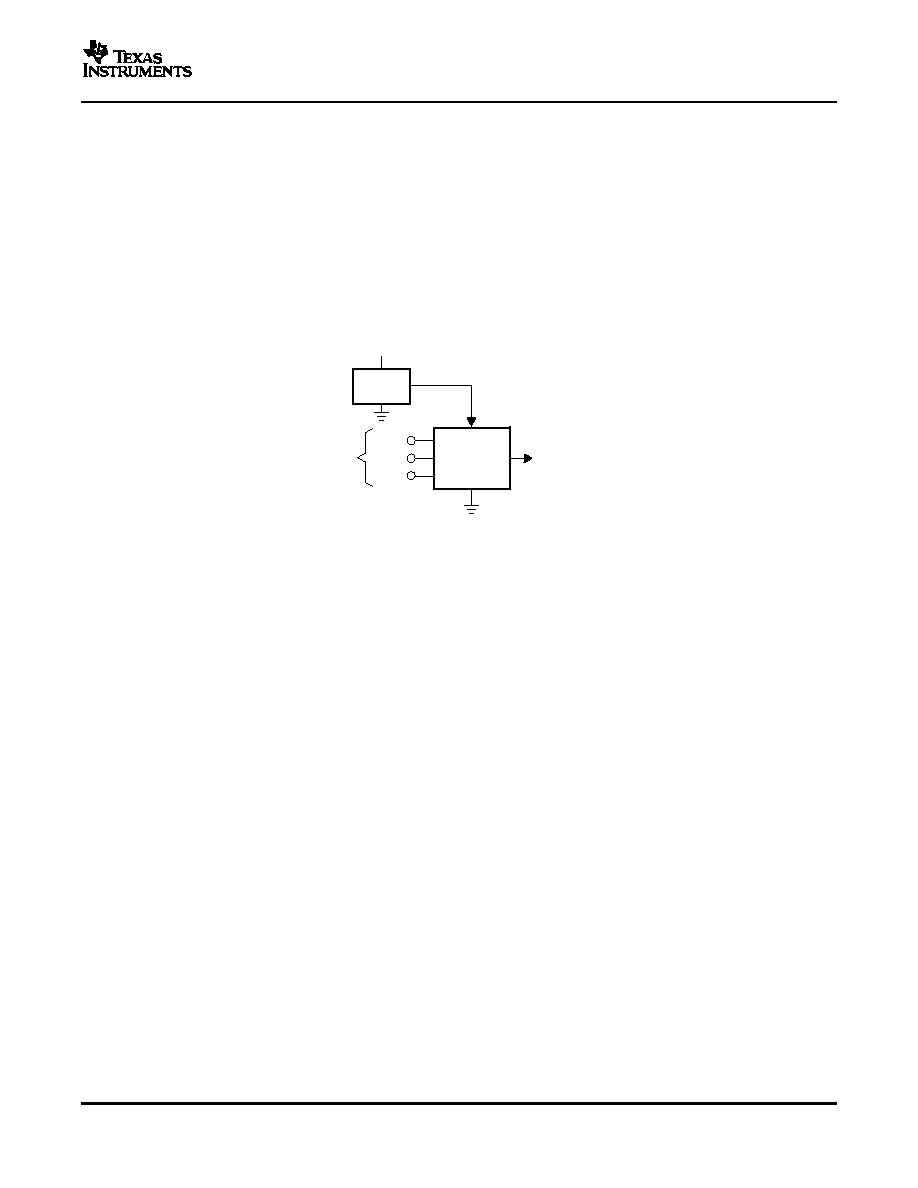
Resistor
String DAC
Powerdown
Circuitry
V
OUT
Amplifier
Resistor
Network
CURRENT CONSUMPTION
DRIVING RESISTIVE AND CAPACITIVE LOADS
OUTPUT VOLTAGE STABILITY
DAC7571
SLAS374A ≠ FEBRUARY 2003 ≠ REVISED JANUARY 2004
Table 2. Modes of Operation for the DAC7571
PD1
PD0
OPERATING MODE
0
0
Normal Operation
0
1
1k
to AGND, PWD
1
0
100k
to AGND, PWD
1
1
High Impedance, PWD
When both bits are set to 0, the device works normally with normal power consumption of 150 µA at 5V.
However, for the three power-down modes, the supply current falls to 200 nA at 5V (50 nA at 3 V). Not only does
the supply current fall but the output stage is also internally switched from the output of the amplifier to a resistor
network of known values. This has the advantage that the output impedance of the device is known while in
power-down mode. There are three different options: The output is connected internally to AGND through a 1 k
resistor, a 100 k
resistor, or it is left open-circuited (high impedance). The output stage is illustrated in
Figure 46.
Figure 46. Output Stage During Power-Down
All linear circuitry is shut down when the power-down mode is activated. However, the contents of the DAC
register are unaffected when in power-down. The time required to exit power down is typically 2.5 µs for AV
DD
=
5 V and 5 µs for AV
DD
= 3V. See the Typical Characteristics for more information.
The DAC7571 typically consumes 150 µA at V
DD
= 5 V and 120 µA at V
DD
= 3 V. Additional current consumption
can occur due to the digital inputs if V
IH
<< V
DD
. For most efficient power operation, CMOS logic levels are
recommended at the digital inputs to the DAC. In power-down mode, typical current consumption is 200 nA. Ten
to 20 ms after a power-down command is issued, the power-down current typically drops below 10 mA.
The DAC7571 output stage is capable of driving loads of up to 1000 pF while remaining stable. Within the offset
and gain error margins, the DAC7571 can operate rail-to-rail when driving a capacitive load. Resistive loads of 2
k
can be driven by the DAC7571 while achieving a typical load regulation of 1%. As the load resistance drops
below 2 k
, the load regulation error increases. When the outputs of the DAC are driven to the positive rail under
resistive loading, the PMOS transistor of each Class-AB output stage can enter into the linear region. When this
occurs, the added IR voltage drop deteriorates the linearity performance of the DAC. This may occur within
approximately the top 20 mV of the DAC's digital input-to-voltage output transfer characteristic.
The DAC7571 exhibits excellent temperature stability of 5 ppm/
∞
C typical output voltage drift over the specified
temperature range of the device. This enables the output voltage to stay within a
±
25 µV window for a
±
1
∞
C
ambient temperature change. Good power-supply rejection ratio (PSRR) performance reduces supply noise
present on V
DD
from appearing at the outputs to well below 10 µV-s. Combined with good dc noise performance
and true 12-bit differential linearity, the DAC7571 becomes a perfect choice for closed-loop control applications.
18
www.ti.com
APPLICATIONS
USING REF02 AS A POWER SUPPLY FOR THE DAC7571
REF02
15 V
5 V
1.14 mA
A0
SCL
SDA
I
2
C
Interface
V
OUT
= 0 V to 5 V
DAC7571
LAYOUT
DAC7571
SLAS374A ≠ FEBRUARY 2003 ≠ REVISED JANUARY 2004
Due to the extremely low supply current required by the DAC7571, a possible configuration is to use a REF02
+5V precision voltage reference to supply the required voltage to the DAC7571's supply input as well as the
reference input, as shown in Figure 47. This is especially useful if the power supply is quite noisy or if the system
supply voltages are at some value other than 5V. The REF02 will output a steady supply voltage for the
DAC7571. If the REF02 is used, the current it needs to supply to the DAC7571 is 150 µA typical and 200 µA max
for V
DD
= 5V. When a DAC output is loaded, the REF02 also needs to supply the current to the load. The total
typical current required (with a 5 mW load on a given DAC output) is: 135 µA + (5 mW/5 V) = 1.14 mA.
The load regulation of the REF02 is typically (0.005%
◊
V
DD
)/mA, which results in an error of 285 mV for the 1.14
mA current drawn from it. This corresponds to a 0.2 LSB error for a 0 V to 5 V output range.
Figure 47. REF02 as Power Supply to DAC7571
A precision analog component requires careful layout, adequate bypassing, and clean, well-regulated power
supplies.
The power applied to V
DD
should be well regulated and low noise. Switching power supplies and DC/DC
converters will often have high-frequency glitches or spikes riding on the output voltage. In addition, digital
components can create similar high-frequency spikes as their internal logic switches states. This noise can easily
couple into the DAC output voltage through various paths between the power connections and analog output.
As with the GND connection, V
DD
should be connected to a +5V power supply plane or trace that is separate
from the connection for digital logic until they are connected at the power entry point. In addition, the 1 µF to 10
µF and 0.1 µF bypass capacitors are strongly recommended. In some situations, additional bypassing may be
required, such as a 100µF electrolytic capacitor or even a Pi filter made up of inductors and capacitors--all
designed to essentially low-pass filter the +5V supply, removing the high-frequency noise.
19


IMPORTANT NOTICE
Texas Instruments Incorporated and its subsidiaries (TI) reserve the right to make corrections, modifications,
enhancements, improvements, and other changes to its products and services at any time and to discontinue
any product or service without notice. Customers should obtain the latest relevant information before placing
orders and should verify that such information is current and complete. All products are sold subject to TI's terms
and conditions of sale supplied at the time of order acknowledgment.
TI warrants performance of its hardware products to the specifications applicable at the time of sale in
accordance with TI's standard warranty. Testing and other quality control techniques are used to the extent TI
deems necessary to support this warranty. Except where mandated by government requirements, testing of all
parameters of each product is not necessarily performed.
TI assumes no liability for applications assistance or customer product design. Customers are responsible for
their products and applications using TI components. To minimize the risks associated with customer products
and applications, customers should provide adequate design and operating safeguards.
TI does not warrant or represent that any license, either express or implied, is granted under any TI patent right,
copyright, mask work right, or other TI intellectual property right relating to any combination, machine, or process
in which TI products or services are used. Information published by TI regarding third-party products or services
does not constitute a license from TI to use such products or services or a warranty or endorsement thereof.
Use of such information may require a license from a third party under the patents or other intellectual property
of the third party, or a license from TI under the patents or other intellectual property of TI.
Reproduction of information in TI data books or data sheets is permissible only if reproduction is without
alteration and is accompanied by all associated warranties, conditions, limitations, and notices. Reproduction
of this information with alteration is an unfair and deceptive business practice. TI is not responsible or liable for
such altered documentation.
Resale of TI products or services with statements different from or beyond the parameters stated by TI for that
product or service voids all express and any implied warranties for the associated TI product or service and
is an unfair and deceptive business practice. TI is not responsible or liable for any such statements.
Following are URLs where you can obtain information on other Texas Instruments products and application
solutions:
Products
Applications
Amplifiers
amplifier.ti.com
Audio
www.ti.com/audio
Data Converters
dataconverter.ti.com
Automotive
www.ti.com/automotive
DSP
dsp.ti.com
Broadband
www.ti.com/broadband
Interface
interface.ti.com
Digital Control
www.ti.com/digitalcontrol
Logic
logic.ti.com
Military
www.ti.com/military
Power Mgmt
power.ti.com
Optical Networking
www.ti.com/opticalnetwork
Microcontrollers
microcontroller.ti.com
Security
www.ti.com/security
Telephony
www.ti.com/telephony
Video & Imaging
www.ti.com/video
Wireless
www.ti.com/wireless
Mailing Address:
Texas Instruments
Post Office Box 655303 Dallas, Texas 75265
Copyright
2004, Texas Instruments Incorporated