1
Æ
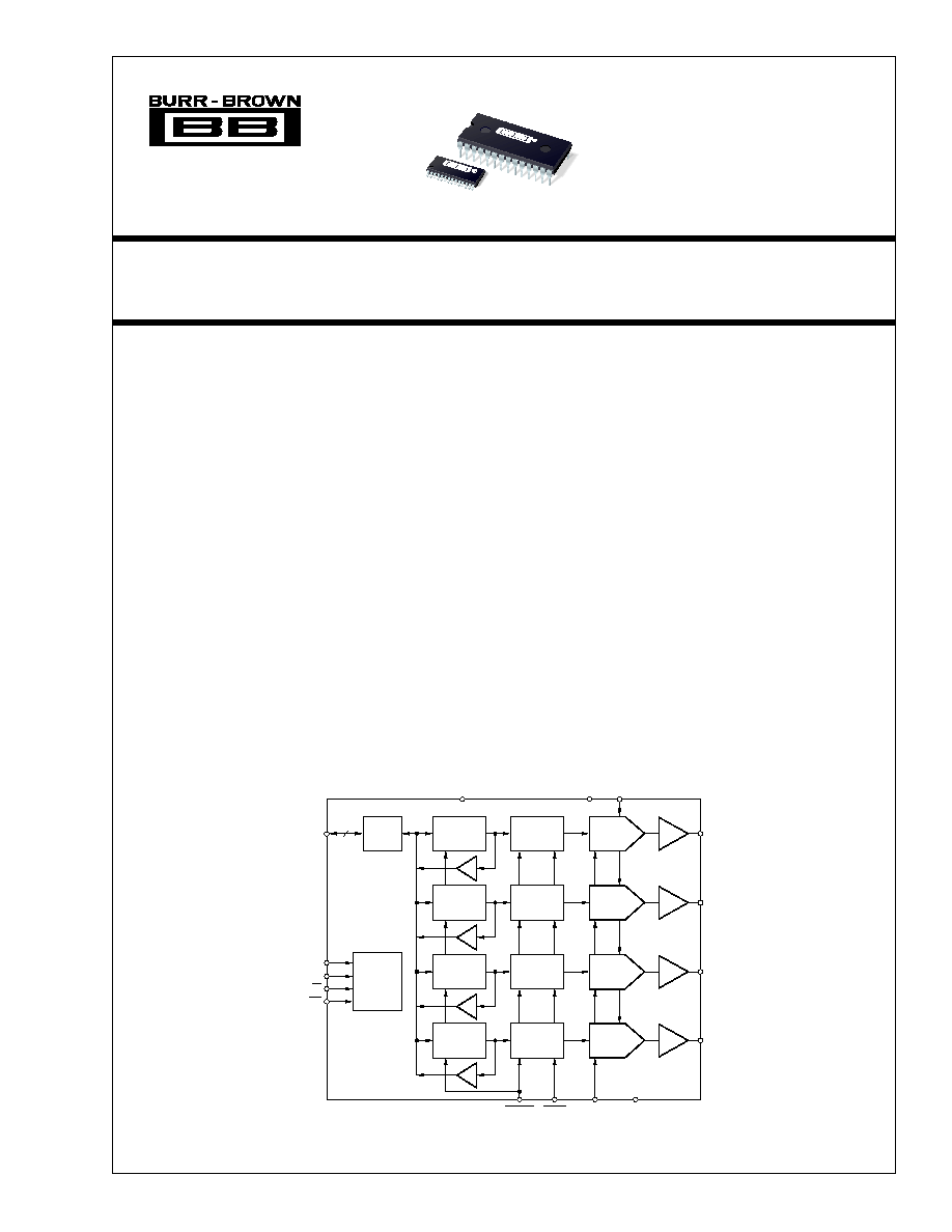
DAC7624/7625
12-Bit Quad Voltage Output
DIGITAL-TO-ANALOG CONVERTER
International Airport Industrial Park ∑ Mailing Address: PO Box 11400, Tucson, AZ 85734 ∑ Street Address: 6730 S. Tucson Blvd., Tucson, AZ 85706 ∑ Tel: (520) 746-1111 ∑ Twx: 910-952-1111
Internet: http://www.burr-brown.com/ ∑ FAXLine: (800) 548-6133 (US/Canada Only) ∑ Cable: BBRCORP ∑ Telex: 066-6491 ∑ FAX: (520) 889-1510 ∑ Immediate Product Info: (800) 548-6132
Æ
DAC7624
DAC7625
DESCRIPTION
The DAC7624 and DAC7625 are 12-bit quad voltage
output digital-to-analog converters with guaranteed 12-
bit monotonic performance over the specified tempera-
ture range. They accept 12-bit parallel input data, have
double-buffered DAC input logic (allowing simulta-
neous update of all DACs), and provide a readback
mode of the internal input registers. An asynchronous
reset clears all registers to a mid-scale code of 800
H
(DAC7624) or to a zero-scale of 000
H
(DAC7625). The
DAC7624 and DAC7625 can operate from a single +5V
supply or from +5V and ≠5V supplies.
Low power and small size per DAC make the DAC7624
and DAC7625 ideal for automatic test equipment,
DAC-per-pin programmers, data acquisition systems,
and closed-loop servo-control. The DAC7624 and
DAC7625 are available in a 28-pin plastic double-
wide or a 28-lead SOIC package, and offer guaranteed
specifications over the ≠40
∞
C to +85
∞
C temperature
range.
FEATURES
q
LOW POWER: 20mW
q
UNIPOLAR OR BIPOLAR OPERATION
q
SETTLING TIME: 10
µ
s to 0.012%
q
12-BIT LINEARITY AND MONOTONICITY:
≠40
∞
C to +85
∞
C
q
RESET TO MID-SCALE (DAC7624) OR
ZERO-SCALE (DAC7625)
q
DATA READBACK
q
DOUBLE-BUFFERED DATA INPUTS
APPLICATIONS
q
PROCESS CONTROL
q
ATE PIN ELECTRONICS
q
CLOSED-LOOP SERVO-CONTROL
q
MOTOR CONTROL
q
DATA ACQUISITION SYSTEMS
q
DAC-PER-PIN PROGRAMMERS
DAC7624
DAC7625
© 1997 Burr-Brown Corporation
PDS-1419C
Printed in U.S.A. April, 2000
DAC A
DAC
Register A
Input
Register A
I/O
Buffer
Control
Logic
DAC B
DAC
Register B
Input
Register B
DAC C
DAC
Register C
Input
Register C
DAC D
DAC
Register D
Input
Register D
V
REFH
V
DD
V
SS
V
OUTD
V
OUTC
V
OUTB
V
OUTA
V
REFL
RESET
LDAC
GND
A0
A1
R/W
CS
DB0-DB11
12
SBAS083
2
Æ
DAC7624/7625
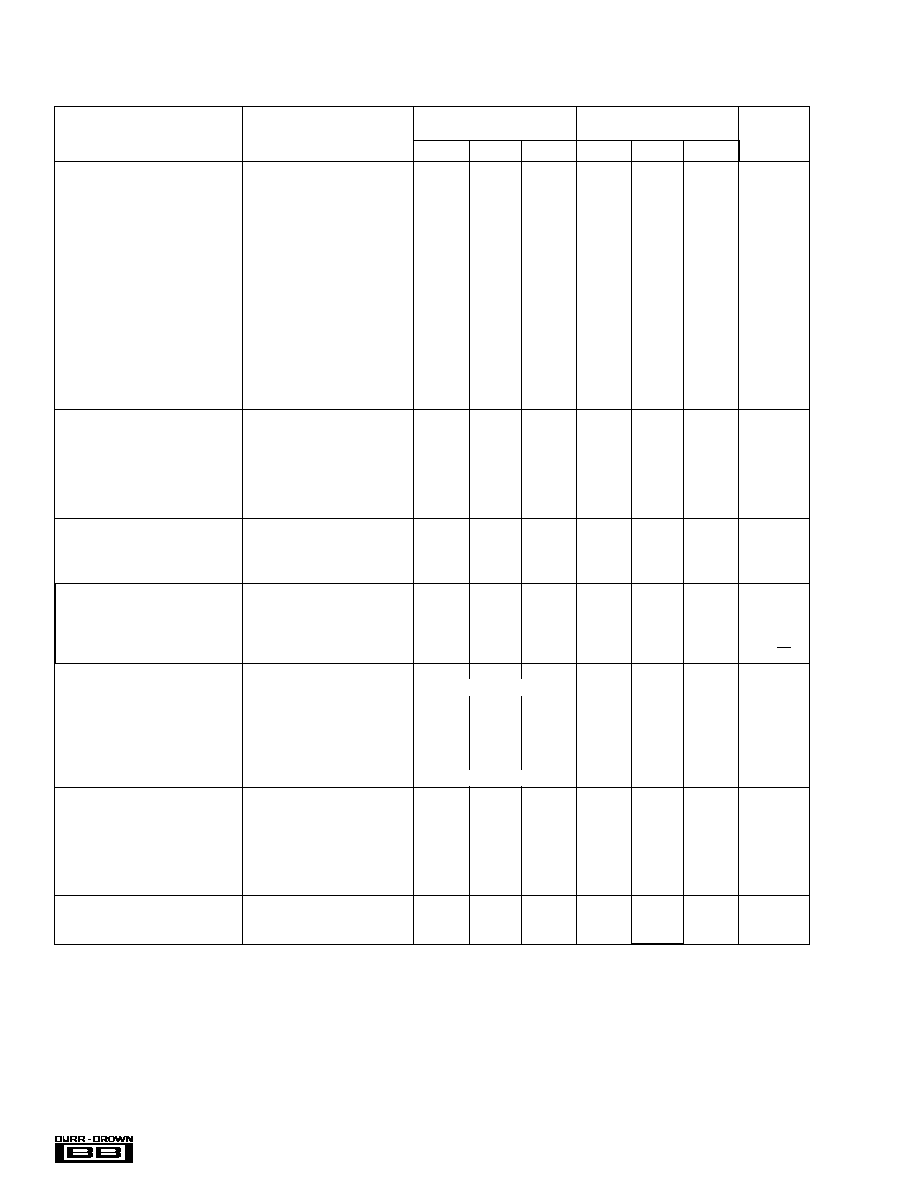
SPECIFICATION
At T
A
= ≠40
∞
C to +85
∞
C, V
DD
= +5V, V
SS
= ≠5V, V
REFH
= +2.5V, V
REFL
= ≠2.5V, unless otherwise noted.
The information provided herein is believed to be reliable; however, BURR-BROWN assumes no responsibility for inaccuracies or omissions. BURR-BROWN assumes
no responsibility for the use of this information, and all use of such information shall be entirely at the user's own risk. Prices and specifications are subject to change
without notice. No patent rights or licenses to any of the circuits described herein are implied or granted to any third party. BURR-BROWN does not authorize or warrant
any BURR-BROWN product for use in life support devices and/or systems.
DAC7624P, U
DAC7624PB, UB
DAC7625P, U
DAC7625PB, UB
NOTES: (1) If V
SS
= 0V, specification applies at code 00A
H
and above. (2) LSB means Least Significant Bit, when V
REFH
equals +2.5V and V
REFL
equals ≠2.5V,
then one LSB equals 1.22mV. (3) All DAC outputs will match within the specified error band. (4) Ideal output voltage, does not take into account zero or full-scale
error. (5) If V
SS
= ≠5V, full-scale 5V step. If V
SS
= 0V, full-scale positive 2.5V step and negative step from code FFF
H
to 00A
H
.
PARAMETER
CONDITIONS
MIN
TYP
MAX
MIN
TYP
MAX
UNITS
ACCURACY
Linearity Error
(1)
V
SS
= 0V or ≠5V
±
2
±
1
LSB
(2)
Linearity Matching
(3)
V
SS
= 0V or ≠5V
±
2
±
1
LSB
Differential Linearity Error
V
SS
= 0V or ≠5V
±
1
±
1
LSB
Monotonicity
T
MIN
to T
MAX
12
T
Bits
Zero-Scale Error
Code = 000
H
±
4
T
LSB
Zero-Scale Drift
2
5
T
T
ppm/
∞
C
Zero-Scale Matching
(3)
±
2
±
1
LSB
Full-Scale Error
Code = FFF
H
±
4
T
LS
Full-Scale Matching
(3)
±
2
±
1
LSB
Zero-Scale Error
Code = 00A
H
, V
SS
= 0V
±
8
T
LSB
Zero-Scale Drift
V
SS
= 0V
5
10
T
T
ppm/
∞
C
Zero-Scale Matching
(3)
V
SS
= 0V
±
4
±
2
LSB
Full-Scale Error
Code = FFF
H
, V
SS
= 0V
±
8
T
LSB
Full-Scale Matching
(3)
V
SS
= 0V
±
4
±
2
LSB
Power Supply Rejection
30
T
ppm /V
ANALOG OUTPUT
Voltage Output
(4)
V
REFL
= 0V, V
SS
= 0V
0
V
REFH
T
T
V
V
SS
= ≠5V
V
REFL
V
REFH
T
T
V
Output Current
≠1.25
+1.25
T
T
mA
Load Capacitance
No Oscillation
100
T
pF
Short-Circuit Current
+5, ≠120
T
mA
Short-Circuit Duration
Momentary
T
REFERENCE INPUT
V
REFH
Input Range
V
SS
= 0V or ≠5V
V
REFL
+1.25
+2.5
T
T
V
V
REFL
Input Range
V
SS
= 0V
0
V
REFH
≠1.25
T
T
V
V
REFL
Input Range
V
SS
= ≠5V
≠2.5
V
REFH
≠1.25
T
T
V
DYNAMIC PERFORMANCE
Settling Time
(5)
To
±
0.012%
5
10
T
T
µ
s
Channel-to-Channel Crosstalk
Full-Scale Step
0.25
T
LSB
On any other DAC
Output Noise Voltage
0Hz to 1MHz
40
T
nV/
Hz
DIGITAL INPUT/OUTPUT
Logic Family
TTL-Compatible CMOS
T
Logic Levels
V
IH
I
IH
±
10
µ
A
2.4
V
DD
+0.3
T
T
V
V
IL
I
IL
±
10
µ
A
≠0.3
0.8
T
T
V
V
OH
I
OH
= ≠0.8mA
3.6
V
DD
T
T
V
V
OL
I
OL
= 1.6mA
0.0
0.4
T
T
V
Data Format
Straight Binary
T
POWER SUPPLY REQUIREMENTS
V
DD
4.75
5.25
T
T
V
V
SS
If V
SS
0V
≠5.25
≠4.75
T
T
V
I
DD
1.5
1.9
T
T
mA
I
SS
≠2.1
≠1.6
T
T
mA
Power Dissipation
V
SS
= ≠5V
15
20
T
T
mW
V
SS
= 0V
7.5
10
T
T
mW
TEMPERATURE RANGE
Specified Performance
DAC7624P, U, PB, UB
≠40
+85
T
T
∞
C
DAC7625P, U, PB, UB
3
Æ
DAC7624/7625
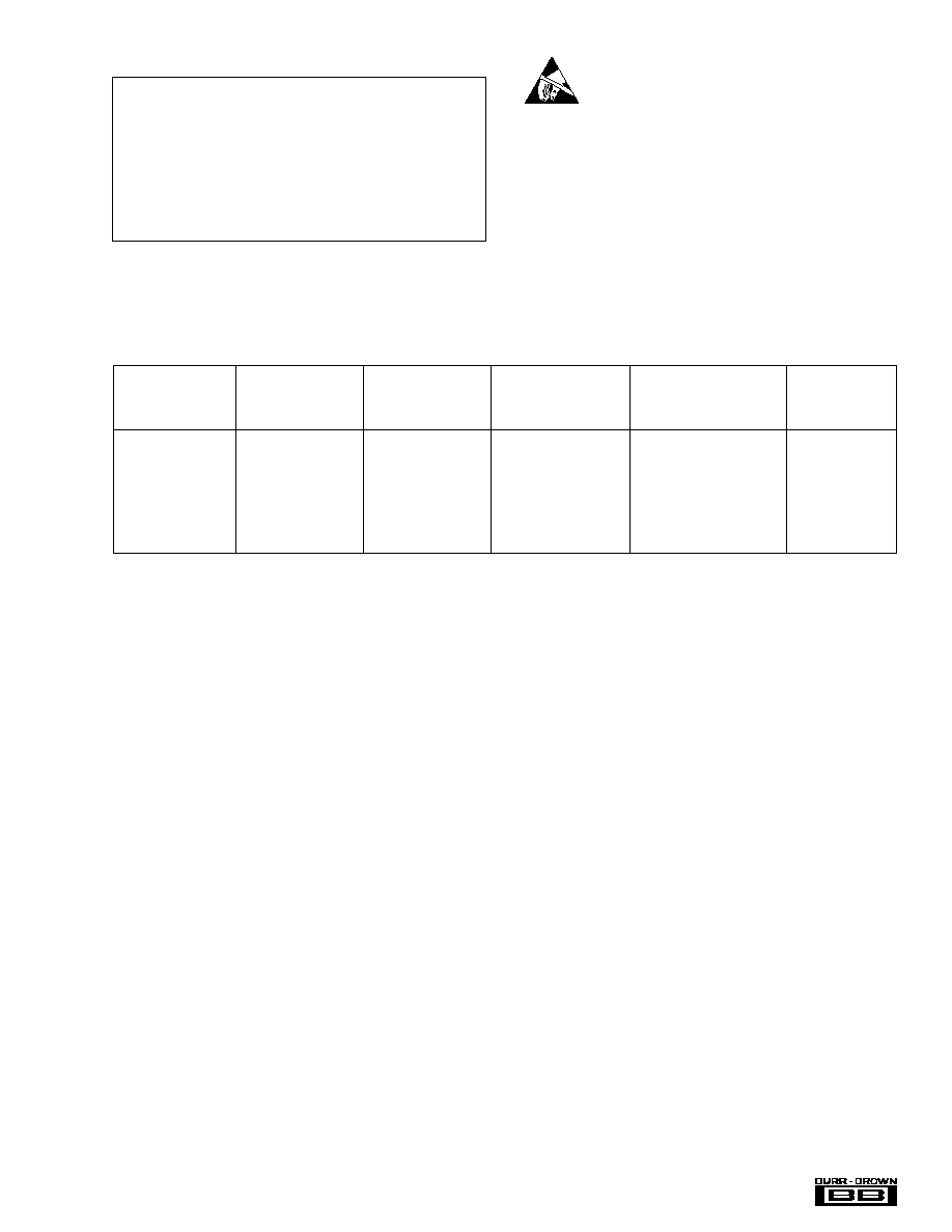
ABSOLUTE MAXIMUM RATINGS
(1)
V
DD
to V
SS
............................................................................. ≠0.3V to 11V
V
DD
to GND .......................................................................... ≠0.3V to 5.5V
V
REFL
to V
SS
.............................................................. ≠0.3V to (V
DD
≠ V
SS
)
V
DD
to V
REFH
............................................................. ≠0.3V to (V
DD
≠ V
SS
)
V
REFH
to V
REFL
.......................................................... ≠0.3V to (V
DD
≠ V
SS
)
Digital Input Voltage to GND ................................... ≠0.3V to V
DD
+ 0.3V
Digital Output Voltage to GND ................................. ≠0.3V to V
DD
+ 0.3V
Maximum Junction Temperature ................................................... +150
∞
C
Operating Temperature Range ........................................ ≠40
∞
C to +85
∞
C
Storage Temperature Range ......................................... ≠65
∞
C to +150
∞
C
Lead Temperature (soldering, 10s) ............................................... +300
∞
C
NOTE: (1) Stresses above those listed under "Absolute Maximum Ratings"
may cause permanent damage to the device. Exposure to absolute maximum
conditions for extended periods may affect device reliability.
ELECTROSTATIC
DISCHARGE SENSITIVITY
This integrated circuit can be damaged by ESD. Burr-Brown
recommends that all integrated circuits be handled with
appropriate precautions. Failure to observe proper handling
and installation procedures can cause damage.
ESD damage can range from subtle performance degradation
to complete device failure. Precision integrated circuits may
be more susceptible to damage because very small parametric
changes could cause the device not to meet its published
specifications.
PACKAGE/ORDERING INFORMATION
MAXIMUM
MAXIMUM
DIFFERENTIAL
SPECIFICATION
PACKAGE
LINEARITY
LINEARITY
TEMPERATURE
DRAWING
PRODUCT
ERROR (LSB)
ERROR (LSB)
RANGE
PACKAGE
NUMBER
(1)
DAC7624P
±
2
±
1
≠40
∞
C to +85
∞
C
28-Pin Plastic DIP
215
DAC7624U
±
2
±
1
≠40
∞
C to +85
∞
C
28-Lead SOIC
217
DAC7624PB
±
1
±
1
≠40
∞
C to +85
∞
C
28-Pin Plastic DIP
215
DAC7624UB
±
1
±
1
≠40
∞
C to +85
∞
C
28-Lead SOIC
217
DAC7625P
±
2
±
1
≠40
∞
C to +85
∞
C
28-Pin Plastic DIP
215
DAC7625U
±
2
±
1
≠40
∞
C to +85
∞
C
28-Lead SOIC
217
DAC7625PB
±
1
±
1
≠40
∞
C to +85
∞
C
28-Pin Plastic DIP
215
DAC7625UB
±
1
±
1
≠40
∞
C to +85
∞
C
28-Lead SOIC
217
NOTE: (1) For detailed drawing and dimension table, please see end of data sheet, or Appendix C of Burr-Brown IC Data Book.
4
Æ
DAC7624/7625
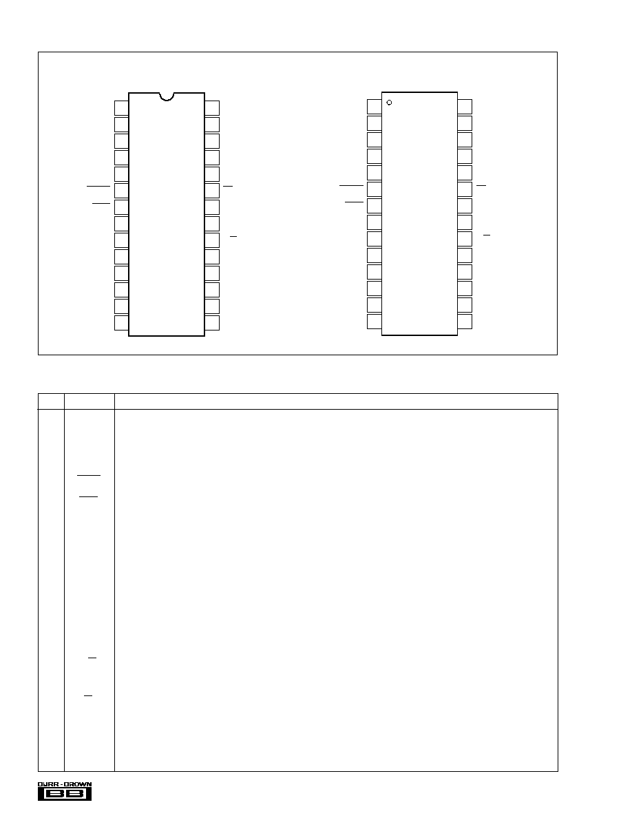
1
2
3
4
5
6
7
8
9
10
11
12
13
14
V
REFH
V
OUTB
V
OUTA
V
SS
GND
RESET
LDAC
(LSB) DB0
DB1
DB2
DB3
DB4
DB5
DB6
V
REFL
V
OUTC
V
OUTD
V
DD
NIC
CS
A0
A1
R/W
DB11 (MSB)
DB10
DB9
DB8
DB7
28
27
26
25
24
23
22
21
20
19
18
17
16
15
DAC7624
DAC7625
1
2
3
4
5
6
7
8
9
10
11
12
13
14
V
REFH
V
OUTB
V
OUTA
V
SS
GND
RESET
LDAC
(LSB) DB0
DB1
DB2
DB3
DB4
DB5
DB6
V
REFL
V
OUTC
V
OUTD
V
DD
NIC
CS
A0
A1
R/W
DB11 (MSB)
DB10
DB9
DB8
DB7
28
27
26
25
24
23
22
21
20
19
18
17
16
15
DAC7624
DAC7625
Top View
DIP
SOIC
PIN DESCRIPTIONS
PIN CONFIGURATIONS
PIN
NAME
DESCRIPTION
1
V
REFH
Reference Input Voltage High. Sets maximum output voltage for all DACs.
2
V
OUTB
DAC B Voltage Output.
3
V
OUTA
DAC A Voltage Output.
4
V
SS
Negative Analog Supply Voltage, 0V or ≠5V.
5
GND
Ground.
6
RESET
Asynchronous Reset Input. Sets DAC and input registers to either mid-scale (800
H
, DAC7624) or zero-scale (000
H
, DAC7625)
when LOW.
7
LDAC
Load DAC Input. All DAC Registers are transparent when LOW.
8
DB0
Data Bit 0. Least significant bit of 12-bit word.
9
DB1
Data Bit 1
10
DB2
Data Bit 2
11
DB3
Data Bit 3
12
DB4
Data Bit 4
13
DB5
Data Bit 5
14
DB6
Data Bit 6
15
DB7
Data Bit 7
16
DB8
Data Bit 8
17
DB9
Data Bit 9
18
DB10
Data Bit 10
19
DB11
Data Bit 11. Most significant bit of 12-bit word.
20
R/W
Read/Write Control Input (read = HIGH, write = LOW).
21
A1
Register/DAC Select (C or D = HIGH, A or B = LOW).
22
A0
Register/DAC Select (B or D = HIGH, A or C = LOW).
23
CS
Chip Select Input.
24
NIC
Not Internally Connected. Pin has no internal connection to the device.
25
V
DD
Positive Analog Supply Voltage, +5V nominal.
26
V
OUTD
DAC D Voltage Output.
27
V
OUTC
DAC C Voltage Output.
28
V
REFL
Reference Input Voltage Low. Sets minimum output voltage for all DACs.
5
Æ
DAC7624/7625
TYPICAL PERFORMANCE CURVES: V
SS
= 0V
At T
A
= +25
∞
C, V
DD
= +5V, V
SS
= 0V, V
REFH
= +2.5V, V
REFL
= 0V, representative unit, unless otherwise specified.
LINEARITY ERROR AND
DIFFERENTIAL LINEARITY ERROR vs CODE
(DAC A)
200
H
000
H
FFF
H
Digital Input Code
DLE (LSB)
LE (LSB)
0.50
0.00
≠0.25
≠0.50
0.50
0.25
0.00
≠0.50
≠0.25
0.25
400
H
600
H
800
H
A00
H
C00
H
E00
H
LINEARITY ERROR AND
DIFFERENTIAL LINEARITY ERROR vs CODE
(DAC B)
200
H
000
H
FFF
H
Digital Input Code
DLE (LSB)
LE (LSB)
0.50
0.00
≠0.25
≠0.50
0.50
0.25
0.00
≠0.50
≠0.25
0.25
400
H
600
H
800
H
A00
H
C00
H
E00
H
LINEARITY ERROR AND
DIFFERENTIAL LINEARITY ERROR vs CODE
(DAC C)
200
H
000
H
FFF
H
Digital Input Code
DLE (LSB)
LE (LSB)
0.50
0.00
≠0.25
≠0.50
0.50
0.25
0.00
≠0.50
≠0.25
0.25
400
H
600
H
800
H
A00
H
C00
H
E00
H
LINEARITY ERROR AND
DIFFERENTIAL LINEARITY ERROR vs CODE
(DAC D)
200
H
000
H
FFF
H
Digital Input Code
DLE (LSB)
LE (LSB)
0.50
0.00
≠0.25
≠0.50
0.50
0.25
0.00
≠0.50
≠0.25
0.25
400
H
600
H
800
H
A00
H
C00
H
E00
H
LINEARITY ERROR vs CODE
(DAC A, ≠40∞C and +85∞C)
200
H
000
H
FFF
H
Digital Input Code
LE (LSB)
LE (LSB)
0.50
0.00
≠0.25
≠0.50
0.50
0.25
0.00
≠0.50
≠0.25
0.25
400
H
600
H
800
H
A00
H
C00
H
E00
H
+85∞C
≠40∞C
LINEARITY ERROR vs CODE
(DAC B, ≠40∞C and +85∞C)
200
H
000
H
FFF
H
Digital Input Code
LE (LSB)
LE (LSB)
0.50
0.00
≠0.25
≠0.50
0.50
0.25
0.00
≠0.50
≠0.25
0.25
400
H
600
H
800
H
A00
H
C00
H
E00
H
+85∞C
≠40∞C
6
Æ
DAC7624/7625
TYPICAL PERFORMANCE CURVES: V
SS
= 0V
(CONT)
At T
A
= +25
∞
C, V
DD
= +5V, V
SS
= 0V, V
REFH
= +2.5V, V
REFL
= 0V, representative unit, unless otherwise specified.
LINEARITY ERROR vs CODE
(DAC C, ≠40∞C and +85∞C)
200
H
000
H
FFF
H
Digital Input Code
LE (LSB)
LE (LSB)
0.50
0.00
≠0.25
≠0.50
0.50
0.25
0.00
≠0.50
≠0.25
0.25
400
H
600
H
800
H
A00
H
C00
H
E00
H
+85∞C
≠40∞C
LINEARITY ERROR vs CODE
(DAC D, ≠40∞C and +85∞C)
200
H
000
H
FFF
H
Digital Input Code
LE (LSB)
LE (LSB)
0.50
0.00
≠0.25
≠0.50
0.50
0.25
0.00
≠0.50
≠0.25
0.25
400
H
600
H
800
H
A00
H
C00
H
E00
H
+85∞C
≠40∞C
ZERO-SCALE ERROR vs TEMPERATURE
(Code 010
H
)
20
≠40
100
≠20
0
40
Temperature (∞C)
Zero-Scale Error (LSB)
≠2
6
4
3
0
≠1
5
1
2
60
80
DAC D
DAC B
DAC C
DAC A
FULL-SCALE ERROR vs TEMPERATURE
(Code FFF
H
)
20
≠40
100
≠20
0
40
Temperature (∞C)
Full-Scale Error (LSB)
≠2
6
4
3
0
≠1
5
1
2
60
80
DAC D
DAC B
DAC C
DAC A
7
Æ
DAC7624/7625
TYPICAL PERFORMANCE CURVES: V
SS
= ≠5V
At T
A
= +25
∞
C, V
DD
= +5V, V
SS
= ≠5V, V
REFH
= +2.5V, V
REFL
= ≠2.5V, representative unit, unless otherwise specified.
LINEARITY ERROR AND
DIFFERENTIAL LINEARITY ERROR vs CODE
(DAC A)
200
H
000
H
FFF
H
Digital Input Code
DLE (LSB)
LE (LSB)
0.50
0.00
≠0.25
≠0.50
0.50
0.25
0.00
≠0.50
≠0.25
0.25
400
H
600
H
800
H
A00
H
C00
H
E00
H
LINEARITY ERROR AND
DIFFERENTIAL LINEARITY ERROR vs CODE
(DAC B)
200
H
000
H
FFF
H
Digital Input Code
DLE (LSB)
LE (LSB)
0.50
0.00
≠0.25
≠0.50
0.50
0.25
0.00
≠0.50
≠0.25
0.25
400
H
600
H
800
H
A00
H
C00
H
E00
H
LINEARITY ERROR AND
DIFFERENTIAL LINEARITY ERROR vs CODE
(DAC C)
200
H
000
H
FFF
H
Digital Input Code
DLE (LSB)
LE (LSB)
0.50
0.00
≠0.25
≠0.50
0.50
0.25
0.00
≠0.50
≠0.25
0.25
400
H
600
H
800
H
A00
H
C00
H
E00
H
LINEARITY ERROR AND
DIFFERENTIAL LINEARITY ERROR vs CODE
(DAC D)
200
H
000
H
FFF
H
Digital Input Code
DLE (LSB)
LE (LSB)
0.50
0.00
≠0.25
≠0.50
0.50
0.25
0.00
≠0.50
≠0.25
0.25
400
H
600
H
800
H
A00
H
C00
H
E00
H
LINEARITY ERROR vs CODE
(DAC A, ≠40∞C and +85∞C)
200
H
000
H
FFF
H
Digital Input Code
LE (LSB)
LE (LSB)
0.50
0.00
≠0.25
≠0.50
0.50
+85∞C
≠40∞C
0.25
0.00
≠0.50
≠0.25
0.25
400
H
600
H
800
H
A00
H
C00
H
E00
H
LINEARITY ERROR vs CODE
(DAC B, ≠40∞C and +85∞C)
200
H
000
H
FFF
H
Digital Input Code
LE (LSB)
LE (LSB)
0.50
0.00
≠0.25
≠0.50
0.50
+85∞C
≠40∞C
0.25
0.00
≠0.50
≠0.25
0.25
400
H
600
H
800
H
A00
H
C00
H
E00
H
8
Æ
DAC7624/7625
TYPICAL PERFORMANCE CURVES: V
SS
= ≠5V
(CONT)
At T
A
= +25
∞
C, V
DD
= +5V, V
SS
= ≠5V, V
REFH
= +2.5V, V
REFL
= ≠2.5V, representative unit, unless otherwise specified.
LINEARITY ERROR vs CODE
(DAC C, ≠40∞C and +85∞C)
200
H
000
H
FFF
H
Digital Input Code
LE (LSB)
LE (LSB)
0.50
0.00
≠0.25
≠0.50
0.50
+85∞C
≠40∞C
0.25
0.00
≠0.50
≠0.25
0.25
400
H
600
H
800
H
A00
H
C00
H
E00
H
LINEARITY ERROR vs CODE
(DAC D, ≠40∞C and +85∞C)
200
H
000
H
FFF
H
Digital Input Code
LE (LSB)
LE (LSB)
0.50
0.00
≠0.25
≠0.50
0.50
+85∞C
≠40∞C
0.25
0.00
≠0.50
≠0.25
0.25
400
H
600
H
800
H
A00
H
C00
H
E00
H
ZERO-SCALE ERROR vs TEMPERATURE
(Code 000
H
)
20
≠40
100
≠20
0
40
Temperature (∞C)
Zero-Scale Error (LSB)
≠1.0
3.0
2.0
1.5
0.0
≠0.5
2.5
0.5
1.0
60
80
DAC D
DAC B
DAC C
DAC A
FULL-SCALE ERROR vs TEMPERATURE
(Code FFF
H
)
20
≠40
100
≠20
0
40
Temperature (∞C)
Full-Scale Error (LSB)
≠1.0
3.0
2.0
1.5
0.0
≠0.5
2.5
0.5
1.0
60
80
DAC D
DAC B
DAC C
DAC A
9
Æ
DAC7624/7625
1
2
3
4
V
REFH
V
OUTB
Load DAC Registers
Reset DACs
(1)
V
OUTA
V
SS
5
GND
6
RESET
7
8
9
10
11
12
13
14
LDAC
DB0
DB1
DB2
DB3
DB4
DB5
DB6
V
REFL
V
OUTC
DAC7624
DAC7625
V
OUTD
V
DD
28
27
26
25
NIC
24
CS
23
A0
A1
R/W
DB11
DB10
DB9
DB8
DB7
22
21
20
19
18
17
16
15
Chip Select
≠2.5V to +2.5V
≠2.5V to +2.5V
Read/Write
Data Bus
Address Bus
or Decoder
NOTE: (1) Reset LOW sets all DACs to code 800
H
on the DAC7624 and to code 000
H
on the DAC7625.
≠2.500V
0.1µF
+5V
0.1µF
1µF to 10µF
+
≠2.5V to +2.5V
≠2.5V to +2.5V
≠5V
+2.500V
0.1µF
0.1µF
1µF to 10µF
+
Data Bus
1
2
3
4
V
REFH
V
OUTB
Load DAC Registers
Reset DACs
(1)
V
OUTA
V
SS
5
GND
6
RESET
7
8
9
10
11
12
13
14
LDAC
DB0
DB1
DB2
DB3
DB4
DB5
DB6
V
REFL
V
OUTC
DAC7624
DAC7625
V
OUTD
V
DD
28
27
26
25
NIC
24
CS
23
A0
A1
R/W
DB11
DB10
DB9
DB8
DB7
22
21
20
19
18
17
16
15
Chip Select
Read/Write
Data Bus
Data Bus
Address Bus
or Decoder
+5V
NOTE: (1) Reset LOW sets all DACs to code 800
H
on the DAC7624 and to code 000
H
on the DAC7625.
0V to +2.5V
0V to +2.5V
0V to +2.5V
0V to +2.5V
0.1µF
1µF to 10µF
+
+2.500V
0.1µF
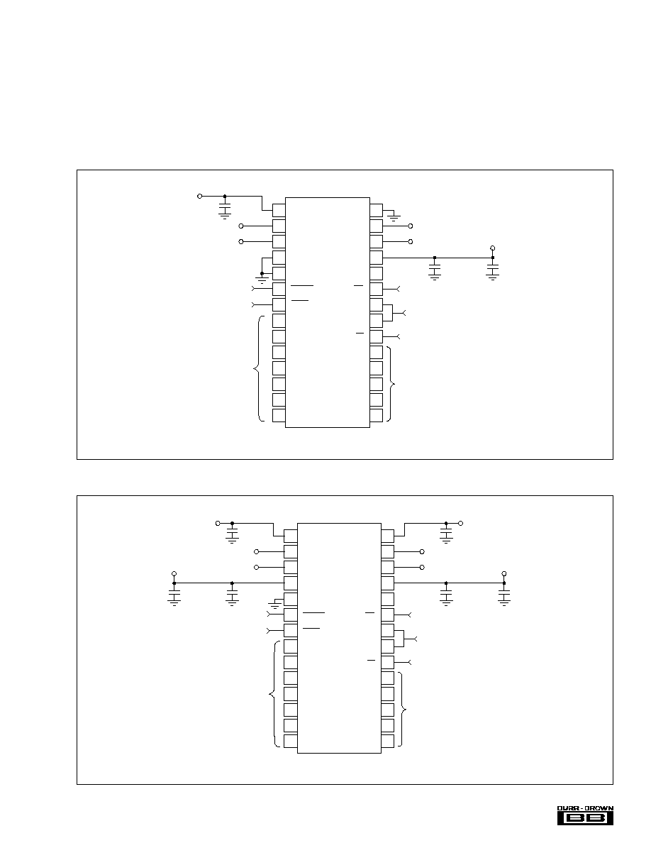
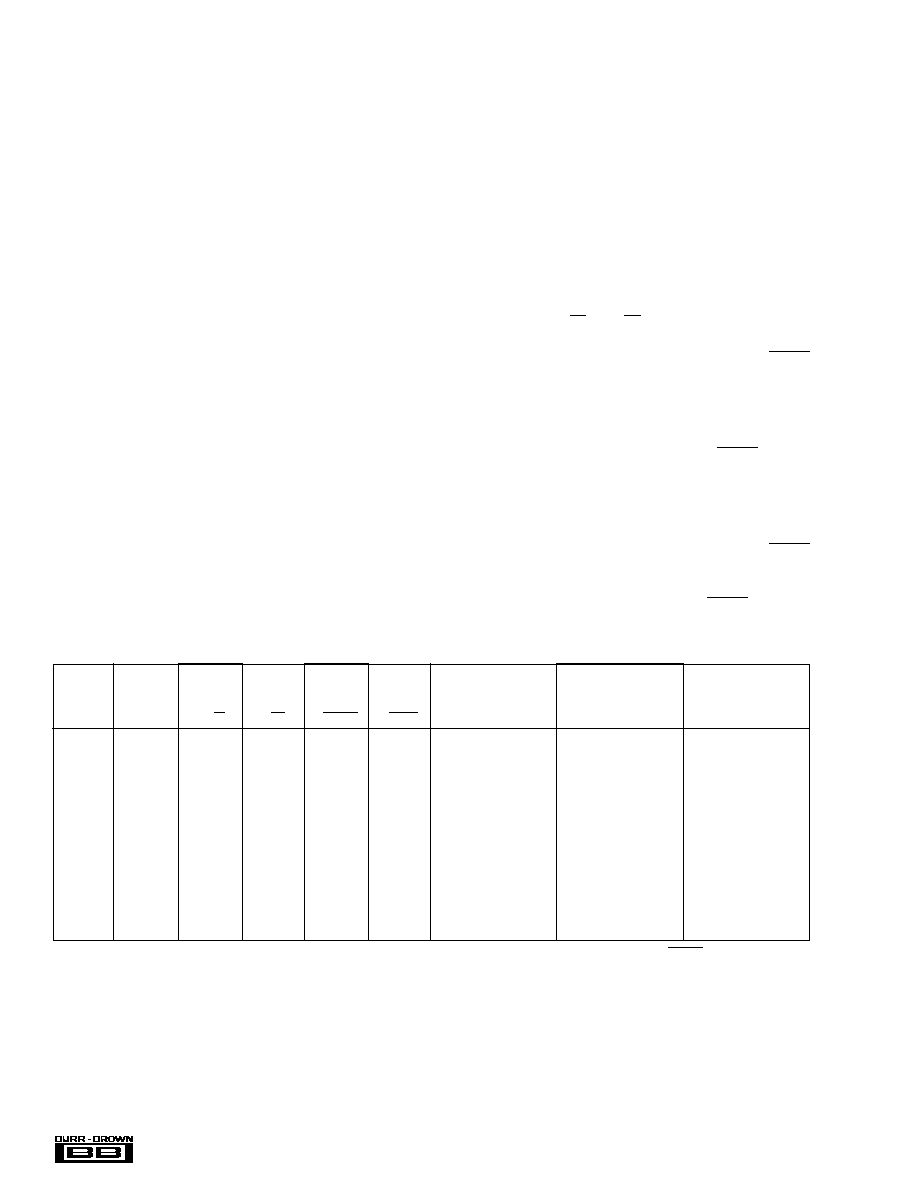
THEORY OF OPERATION
The DAC7624 and DAC7625 are quad, voltage output,
12-bit digital-to-analog converters (DACs). The architecture
is a classic R-2R ladder configuration followed by an opera-
tional amplifier that serves as a buffer. Each DAC has its
own R-2R ladder network and output op-amp, but all share
the reference voltage inputs. The minimum voltage output
("zero-scale") and maximum voltage output ("full-scale")
are set by the external voltage references (V
REFL
and V
REFH
,
respectively). The digital input is a 12-bit parallel word and
the DAC input registers offer a readback capability. The
converters can be powered from a single +5V supply or a
dual
±
5V supply. Each device offers a reset function which
immediately sets all DAC output voltages and DAC regis-
ters to mid-scale (DAC7624, code 800
H
) or to zero-scale
(DAC7625, code 000
H
). See Figures 1 and 2 for the basic
operation of the DAC7624/25.
FIGURE 1. Basic Single-Supply Operation of the DAC7624/25.
FIGURE 2. Basic Dual-Supply Operation of the DAC7624/25.
10
Æ
DAC7624/7625
ANALOG OUTPUTS
When V
SS
= ≠5V (dual supply operation), the output ampli-
fier can swing to within 2.25V of the supply rails, guaran-
teed over the ≠40
∞
C to +85
∞
C temperature range. With V
SS
= 0V (single-supply operation), the output can swing to
ground. Note that the settling time of the output op-amp will
be longer with voltages very near ground. Also, care must be
taken when measuring the zero-scale error when V
SS
= 0V.
Since the output voltage cannot swing below ground, the
output voltage may not change for the first few digital input
codes (000
H
, 001
H
, 002
H
, etc.) if the output amplifier has a
negative offset.
The behavior of the output amplifier can be critical in some
applications. Under short circuit conditions (DAC output
shorted to ground), the output amplifier can sink a great deal
more current than it can source. See the specification table
for more details concerning short circuit current.
REFERENCE INPUTS
The reference inputs, V
REFL
and V
REFH
, can be any voltage
between V
SS
+2.25V and V
DD
≠2.25V provided that V
REFH
is
at least 1.25V greater than V
REFL
. The minimum output of
each DAC is equal to V
REFL
plus a small offset voltage
(essentially, the offset of the output op-amp). The maximum
output is equal to V
REFH
plus a similar offset voltage. Note
that V
SS
(the negative power supply) must either be
connected to ground or must be in the range of ≠4.75V to
≠5.25V. The voltage on V
SS
sets several bias points within
the converter, if V
SS
is not in one of these two configura-
tions, the bias values may be in error and proper operation
of the device is not guaranteed.
The current into the V
REFH
input depends on the DAC output
voltages and can vary from a few microamps to approxi-
mately 0.5 milliamp. The V
REFH
source will not be required
to sink current, only source it. Bypassing the reference
voltage or voltages with at least a 0.1uF capacitor placed as
close to the DAC7624/25 package is strongly recommended.
DIGITAL INTERFACE
Table I shows the basic control logic for the DAC7624/25.
Note that each internal register is level triggered and not
edge triggered. When the appropriate signal is LOW, the
register becomes transparent. When this signal is returned
HIGH, the digital word currently in the register is latched.
The first set of registers (the Input Registers) are triggered
via the A0, A1, R/W, and CS inputs. Only one of these
registers is transparent at any given time. The second set of
registers (the DAC Registers) are all transparent when LDAC
input is pulled LOW.
Each DAC can be updated independently by writing to the
appropriate Input Register and then updating the DAC
Register. Alternatively, the entire DAC Register set can be
configured as always transparent by keeping LDAC LOW--
the DAC update will occur when the Input Register is
written.
The double buffered architecture is mainly designed so that
each DAC Input Register can be written at any time and then
all DAC voltages updated simultaneously by pulling LDAC
LOW. It also allows a DAC Input Register to be written to
at any point and the DAC voltage to be synchronously
changed via a trigger signal connected to LDAC.
STATE OF
SELECTED
SELECTED
STATE OF
INPUT
INPUT
ALL DAC
A1
A0
R/W
CS
RESET
LDAC
REGISTER
REGISTER
REGISTERS
L
(1)
L
L
L
H
(2)
L
A
Transparent
Transparent
L
H
L
L
H
L
B
Transparent
Transparent
H
L
L
L
H
L
C
Transparent
Transparent
H
H
L
L
H
L
D
Transparent
Transparent
L
L
L
L
H
H
A
Transparent
Latched
L
H
L
L
H
H
B
Transparent
Latched
H
L
L
L
H
H
C
Transparent
Latched
H
H
L
L
H
H
D
Transparent
Latched
L
L
H
L
H
H
A
Readback
Latched
L
H
H
L
H
H
B
Readback
Latched
H
L
H
L
H
H
C
Readback
Latched
H
H
H
L
H
H
D
Readback
Latched
X
(3)
X
X
H
H
L
NONE
(All Latched)
Transparent
X
X
X
H
H
H
NONE
(All Latched)
Latched
X
X
X
X
L
X
ALL
Reset
(4)
Reset
(4)
NOTES: (1) L = Logic LOW. (2) H= Logic HIGH. (3) X = Don't Care. (4) DAC7624 resets to 800
H
, DAC7625 resets to 000
H
. When RESET rises, all registers that
are in their latched state retain the reset value.
TABLE I. DAC7624 and DAC7625 Control Logic Truth Table.
11
Æ
DAC7624/7625
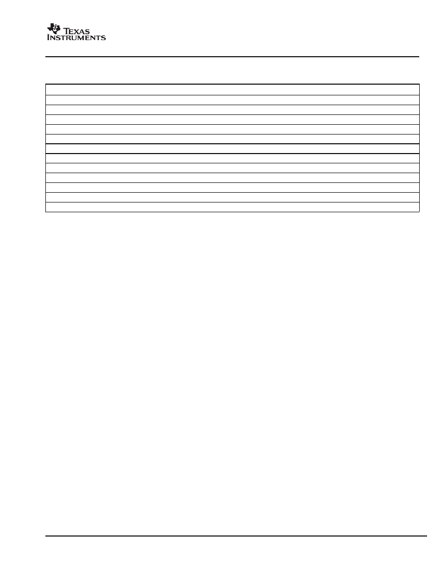
DIGITAL TIMING
Figure 3 and Table II provide detailed timing for the digital
interface of the DAC7624 and DAC7625.
DIGITAL INPUT CODING
The DAC7624 and DAC7625 input data is in straight binary
format. The output voltage is given by the following equa-
tion:
where N is the digital input code. This equation does not
include the effects of offset (zero-scale) or gain (full-scale)
errors.
V
OUT
=
V
REFL
+
V
REFH
≠ V
REFL
(
)
∑ N
4096
t
RCS
CS
t
RDS
t
RDH
t
AS
t
CSD
t
DZ
t
AH
R/W
A0/A1
Data Out
Data Valid
t
WCS
CS
t
WS
t
AS
t
AH
t
WH
R/W
A0/A1
t
RESET
t
LWD
t
LH
LDAC
t
DS
t
DH
t
LS
Data In
RESET
Data Output Timing
Digital Input Timing
FIGURE 3. Digital Input and Output Timing.
SYMBOL
DESCRIPTION
MIN
TYP
MAX
UNITS
t
RCS
CS LOW for Read
200
ns
t
RDS
R/W HIGH to CS LOW
10
ns
t
RDH
R/W HIGH after CS HIGH
0
ns
t
DZ
CS HIGH to Data Bus in High Impedance
100
ns
t
CSD
CS LOW to Data Bus Valid
100
160
ns
t
WCS
CS LOW for Write
50
ns
t
WS
R/W LOW to CS LOW
0
ns
t
WH
R/W LOW after CS HIGH
0
ns
t
AS
Address Valid to CS LOW
0
ns
t
AH
Address Valid after CS HIGH
0
ns
t
LS
LDAC LOW to CS LOW
70
ns
t
LH
LDAC LOW after CS HIGH
50
ns
t
DS
Data Valid to CS LOW
0
ns
t
DH
Data Valid after CS HIGH
0
ns
t
LWD
LDAC LOW
50
ns
t
RESET
RESET LOW
50
ns
TABLE II. Timing Specifications (T
A
= ≠40
∞
C to +85
∞
C).
PACKAGING INFORMATION
ORDERABLE DEVICE
STATUS(1)
PACKAGE TYPE
PACKAGE DRAWING
PINS
PACKAGE QTY
DAC7624P
NRND
PDIP
NTD
28
13
DAC7624PB
NRND
PDIP
NTD
28
13
DAC7624U
ACTIVE
SOIC
DW
28
28
DAC7624U/1K
ACTIVE
SOIC
DW
28
1000
DAC7624UB
ACTIVE
SOIC
DW
28
28
DAC7624UB/1K
ACTIVE
SOIC
DW
28
1000
DAC7625P
NRND
PDIP
NTD
28
13
DAC7625PB
NRND
PDIP
NTD
28
13
DAC7625U
ACTIVE
SOIC
DW
28
28
DAC7625U/1K
ACTIVE
SOIC
DW
28
1000
DAC7625UB
ACTIVE
SOIC
DW
28
28
DAC7625UB/1K
ACTIVE
SOIC
DW
28
1000
(1) The marketing status values are defined as follows:
ACTIVE: Product device recommended for new designs.
LIFEBUY: TI has announced that the device will be discontinued, and a lifetime-buy period is in effect.
NRND: Not recommended for new designs. Device is in production to support existing customers, but TI does not recommend using this part in
a new design.
PREVIEW: Device has been announced but is not in production. Samples may or may not be available.
OBSOLETE: TI has discontinued the production of the device.
PACKAGE OPTION ADDENDUM
www.ti.com
21-Oct-2003

IMPORTANT NOTICE
Texas Instruments Incorporated and its subsidiaries (TI) reserve the right to make corrections, modifications,
enhancements, improvements, and other changes to its products and services at any time and to discontinue
any product or service without notice. Customers should obtain the latest relevant information before placing
orders and should verify that such information is current and complete. All products are sold subject to TI's terms
and conditions of sale supplied at the time of order acknowledgment.
TI warrants performance of its hardware products to the specifications applicable at the time of sale in
accordance with TI's standard warranty. Testing and other quality control techniques are used to the extent TI
deems necessary to support this warranty. Except where mandated by government requirements, testing of all
parameters of each product is not necessarily performed.
TI assumes no liability for applications assistance or customer product design. Customers are responsible for
their products and applications using TI components. To minimize the risks associated with customer products
and applications, customers should provide adequate design and operating safeguards.
TI does not warrant or represent that any license, either express or implied, is granted under any TI patent right,
copyright, mask work right, or other TI intellectual property right relating to any combination, machine, or process
in which TI products or services are used. Information published by TI regarding third-party products or services
does not constitute a license from TI to use such products or services or a warranty or endorsement thereof.
Use of such information may require a license from a third party under the patents or other intellectual property
of the third party, or a license from TI under the patents or other intellectual property of TI.
Reproduction of information in TI data books or data sheets is permissible only if reproduction is without
alteration and is accompanied by all associated warranties, conditions, limitations, and notices. Reproduction
of this information with alteration is an unfair and deceptive business practice. TI is not responsible or liable for
such altered documentation.
Resale of TI products or services with statements different from or beyond the parameters stated by TI for that
product or service voids all express and any implied warranties for the associated TI product or service and
is an unfair and deceptive business practice. TI is not responsible or liable for any such statements.
Following are URLs where you can obtain information on other Texas Instruments products and application
solutions:
Products
Applications
Amplifiers
amplifier.ti.com
Audio
www.ti.com/audio
Data Converters
dataconverter.ti.com
Automotive
www.ti.com/automotive
DSP
dsp.ti.com
Broadband
www.ti.com/broadband
Interface
interface.ti.com
Digital Control
www.ti.com/digitalcontrol
Logic
logic.ti.com
Military
www.ti.com/military
Power Mgmt
power.ti.com
Optical Networking
www.ti.com/opticalnetwork
Microcontrollers
microcontroller.ti.com
Security
www.ti.com/security
Telephony
www.ti.com/telephony
Video & Imaging
www.ti.com/video
Wireless
www.ti.com/wireless
Mailing Address:
Texas Instruments
Post Office Box 655303 Dallas, Texas 75265
Copyright
2003, Texas Instruments Incorporated