Document Outline
- FEATURES
- APPLICATIONS
- DESCRIPTION
- ORDERING INFORMATION(
- ABSOLUTE MAXIMUM RATINGS
- ELECTRICAL CHARACTERISTICS: VSS = 0V
- ELECTRICAL CHARACTERISTICS: VSS = - 5V
- PIN ASSIGNMENTS LQFP PACKAGE
- Terminal Functions
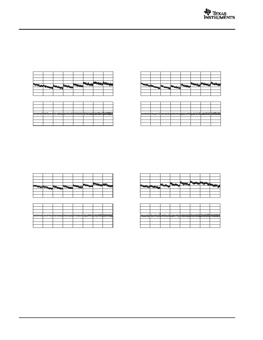
- TYPICAL CHARACTERISTICS: VSS = 0V (+25∞C)
- TYPICAL CHARACTERISTICS: VSS = 0V (+85∞C)
- TYPICAL CHARACTERISTICS: VSS = 0V (-40∞C)
- TYPICAL CHARACTERISTICS: VSS = 0V
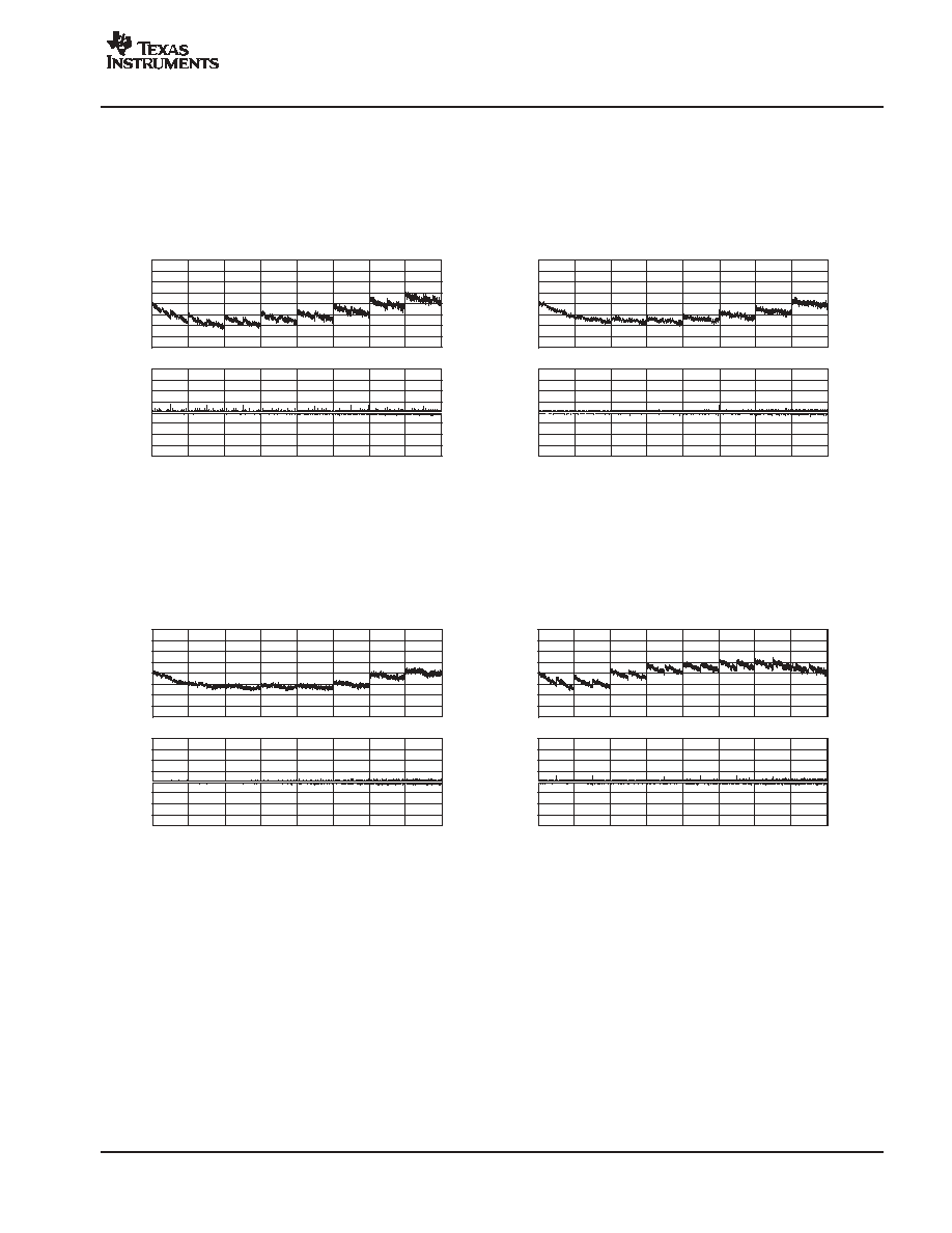
- TYPICAL CHARACTERISTICS: VSS = -5V (+25∞C)
- TYPICAL CHARACTERISTICS: VSS = -5V (+85∞C)
- TYPICAL CHARACTERISTICS: VSS = -5V (-40∞C)
- TYPICAL CHARACTERISTICS: VSS = -5V
- THEORY OF OPERATION
- ANALOG OUTPUTS
- DIGITAL INTERFACE
- 3V TO 5V LOGIC INTERFACE
- GLITCH SUPPRESSION CIRCUIT
- DIGITAL TIMING
- DIGITAL INPUT CODING
SBAS271 - MARCH 2004
16 Bit, Quad Voltage Output
Digital to Analog Converter
DAC7664
FEATURES
D
Low Glitch: 1nV-s (typ)
D
Low Power: 18mW
D
Unipolar or Bipolar Operation
D
Settling Time: 12
µ
s to 0.003%
D
16-Bit Linearity and Monotonicity:
≠40
∞
C to +85
∞
C
D
Programmable Reset to Mid-Scale or
Zero-Scale
D
Data Readback
D
Double-Buffered Data Inputs
D
Internal Bandgap Voltage Reference
D
Power-On Reset
D
3V to 5V Logic Interface
APPLICATIONS
D
Process Control
D
Closed-Loop Servo Control
D
Motor Control
D
Data Acquisition Systems
D
DAC-per-Pin Programmers
DESCRIPTION
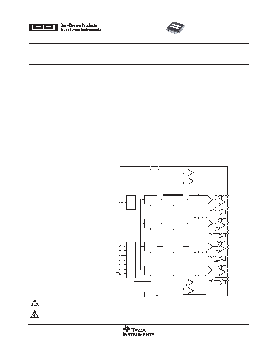
The DAC7664 is a 16-bit, quad voltage output
digital-to-analog converter (DAC) with 16-bit monotonic
performance over the specified temperature range. It
accepts 16-bit parallel input data, has double-buffered
DAC input logic (allowing simultaneous update of all
DACs), and provides a readback mode of the internal input
registers. Programmable asynchronous reset clears all
registers to a mid-scale code of 8000h or to a zero-scale
of 0000h. The DAC7664 can operate from a single +5V
supply or from +5V and -5V supplies.
Low power and small size per DAC make the DAC7664
ideal for automatic test equipment, DAC-per-pin
programmers, data acquisition systems, and closed-loop
servo control. The DAC7664 is available in an LQFP-64
package and is specified for operation over the -40
∞
C to
+85
∞
C temperature range.
This device has ESD-CDM sensitivity and special handling precautions must be taken.
PRODUCTION DATA information is current as of publication date. Products
conform to specifications per the terms of Texas Instruments standard warranty.
Production processing does not necessarily include testing of all parameters.
All trademarks are the property of their respective owners.
www.ti.com
Copyright
2004, Texas Instruments Incorporated
Please be aware that an important notice concerning availability, standard warranty, and use in critical applications of Texas Instruments
semiconductor products and disclaimers thereto appears at the end of this data sheet.
DAC A
DAC
Register A
Bandgap
Voltage Reference
Input
Register A
Data
Latch
DAC B
DAC
Register B
Input
Register B
DAC C
DAC
Register C
Input
Register C
DAC D
DAC
Register D
Input
Register D
V
O U T
A
V
R E F
V
O U T
A
Sense 1
V
O U T
A
Sense 2
DB0-DB15
Control
Logic
RST
CS
A0
A1
RSTSEL
LDAC
R/W
A G ND
D GND
OFSR1A
OFSR2A
V
C C
V
S S
V
D D
DAC7664
V
R E F
L
A and B
V
R E F
H
A and B
V
RE F
H
C
and D
V
R E F
L C
and D
V
O U T
B
V
O U T
B
Sense 1
V
O U T
B
Sense 2
OFSR1B
OFSR2B
V
O U T
C
V
O U T
C
Sense 1
V
O U T
C
Sense 2
OFSR1C
OFSR2C
V
O U T
D
V
O U T
D
Sense 1
V
O U T
D
Sense 2
OFSR1D
OFSR2D
V
R E F
V
R E F
V
R E F

DAC7664
SBAS271 - MARCH 2004
www.ti.com
2
ORDERING INFORMATION
(1)
PRODUCT
PACKAGE-LEAD
PACKAGE
DESIGNATOR
SPECIFIED
TEMPERATURE
RANGE
PACKAGE
MARKING
ORDERING
NUMBER
TRANSPORT
MEDIA, QUANTITY
DAC7664Y
LQFP-64
PM
-40
∞
C to +85
∞
C
DAC7664Y
DAC7664YT
Tape and Reel, 250
DAC7664Y
LQFP-64
PM
-40
∞
C to +85
∞
C
DAC7664Y
DAC7664YR
Tape and Reel, 1500
DAC7664YB
LQFP-64
PM
-40
∞
C to +85
∞
C
DAC7664YB
DAC7664YBT
Tape and Reel, 250
DAC7664YB
LQFP-64
PM
-40
∞
C to +85
∞
C
DAC7664YB
DAC7664YBR
Tape and Reel, 1500
DAC7664YC
LQFP-64
PM
-40
∞
C to +85
∞
C
DAC7664YC
DAC7664YCT
Tape and Reel, 250
DAC7664YC
LQFP-64
PM
-40
∞
C to +85
∞
C
DAC7664YC
DAC7664YCR
Tape and Reel, 1500
(1) For the most current package and ordering information, see the Package Option Addendum located at the end of this data sheet.
ABSOLUTE MAXIMUM RATINGS
over operating free-air temperature range unless otherwise noted(1)
DAC7664
UNIT
IOVDD, VCC and VDD to VSS
-0.3 to 11
V
IOVDD, VCC and VDD to GND
-0.3 to 5.5
V
Digital Input Voltage to GND
-0.3 to VDD + 0.3
V
Digital Output Voltage to GND
-0.3 to VDD + 0.3
V
ESD-CDM
200
V
Maximum Junction Temperature
+150
∞
C
Operating Temperature Range
-40 to +85
∞
C
Storage Temperature Range
-65 to +125
∞
C
Lead Temperature (soldering, 10s)
+300
∞
C
(1) Stresses above those listed under Absolute Maximum Ratings
may cause permanent damage to the device. Exposure to
absolute maximum conditions for extended periods may degrade
device reliability. These are stress ratings only, and functional
operation of the device at these or any other conditions beyond
those specified is not implied.
This integrated circuit can be damaged by ESD. Texas
Instruments recommends that all integrated circuits be
handled with appropriate precautions. Failure to observe
proper handling and installation procedures can cause damage.
ESD damage can range from subtle performance degradation to
complete device failure. Precision integrated circuits may be more
susceptible to damage because very small parametric changes could
cause the device not to meet its published specifications.
DAC7664
SBAS271 - MARCH 2004
www.ti.com
3
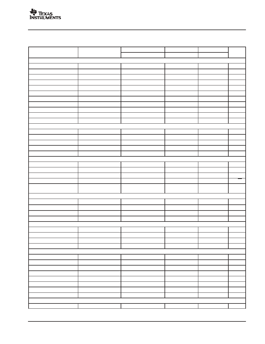
ELECTRICAL CHARACTERISTICS: V
SS
= 0V
All specifications at TA = TMIN to TMAX, IOVDD = VDD = VCC = +5V, and VSS = 0V, unless otherwise noted.
DAC7664Y
DAC7664YB
DAC7664YC
PARAMETER
TEST CONDITIONS
MIN
TYP
MAX
MIN
TYP
MAX
MIN
TYP
MAX
UNIT
Accuracy
Linearity error
±
3
±
4
±
2
±
3
[
[
LSB
Linearity match
±
4
±
2
[
LSB
Differential linearity error
±
2
±
3
±
1
±
2
-1
+2
LSB
Monotonicity, TMIN to TMAX
14
15
16
Bit
Unipolar zero error
±
1
±
5
[
[
[
[
mV
Unipolar zero error drift
5
10
[
[
[
[
ppm/
∞
C
Full-scale error
±
6
±
20
±
4
±
12.5
[
[
mV
Full-scale error drift
7
15
[
[
[
[
ppm/
∞
C
Unipolar zero matching
Channel-to-channel matching
±
3
±
7
±
2
±
5
[
[
mV
Full-scale matching
Channel-to-channel matching
±
4
±
10
±
2
±
8
[
[
mV
Power-supply rejection ratio (PSRR)
At full-scale
10
100
[
[
[
[
ppm/V
Analog Output
Voltage output
RL = 10k
0
2.5
[
[
[
[
V
Output current
-1.25
+1.25
[
[
[
[
mA
Maximum load capacitance
No oscillation
500
[
[
pF
Short-circuit current
±
20
[
[
mA
Short-circuit duration
GND or VCC
Indefinite
[
[
Dynamic Performance
Settling time
To
±
0.003%, 2.5V output step
12
15
[
[
[
[
µ
s
Channel-to-channel crosstalk
0.5
[
[
LSB
Digital feedthrough
2
[
[
nV-s
Output noise voltage
f = 10kHz
130
[
[
nV/
Hz
DAC glitch
7FFFh to 8000h or
8000h to 7FFFh
1
5
[
[
[
[
nV-s
Digital Input
VIH
0.7
◊
IOVDD
[
[
V
VIL
0.3
◊
IOVDD
[
[
V
IIH
±
10
[
[
µ
A
IIL
±
10
[
[
µ
A
Digital Output
VOH
IOH = -0.8mA, IOVDD = 5V
3.6
4.5
[
[
[
[
V
VOL
IOL = 1.6mA, IOVDD = 5V
0.3
0.4
[
[
[
[
V
VOH
IOH = -0.4mA, IOVDD = 3V
2.4
2.6
[
[
[
[
V
VOL
IOL = 0.8mA, IOVDD = 3V
0.3
0.4
[
[
[
[
V
Power Supply
VDD
+4.75
+5.0
+5.25
[
[
[
[
[
[
V
IOVDD
+2.7
+5.0
+5.25
[
[
[
[
[
[
V
VCC
+4.75
+5.0
+5.25
[
[
[
[
[
[
V
VSS
0
0
0
[
[
[
[
[
[
V
ICC
3.5
5
[
[
[
[
mA
IDD
50
[
[
µ
A
I(IOVDD)
50
[
[
µ
A
Power
18
25
[
[
[
mW
Temperature Range
Specified performance
-40
+85
[
[
[
[
∞
C
[
specifications same as the grade to the left
DAC7664
SBAS271 - MARCH 2004
www.ti.com
4
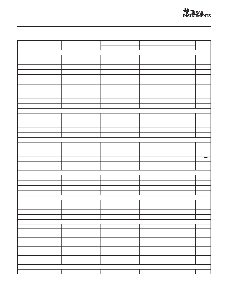
ELECTRICAL CHARACTERISTICS: V
SS
= -5V
All specifications at TA = TMIN to TMAX, IOVDD = VDD = VCC = +5V, and VSS = -5V, unless otherwise noted.
DAC7664Y
DAC7664YB
DAC7664YC
PARAMETER
TEST CONDITIONS
MIN
TYP
MAX
MIN
TYP
MAX
MIN
TYP
MAX
UNIT
Accuracy
Linearity error
±
3
±
4
±
2
±
3
[
[
LSB
Linearity match
±
4
±
2
[
LSB
Differential linearity error
±
2
±
3
±
1
±
2
-1
+2
LSB
Monotonicity, TMIN to TMAX
14
15
16
Bit
Bipolar zero error
±
1
±
5
[
[
[
[
mV
Bipolar zero error drift
5
10
[
[
[
[
ppm/
∞
C
Full-scale error
±
6
±
20
±
4
±
12.5
[
[
mV
Full-scale error drift
7
15
[
[
[
[
ppm/
∞
C
Bipolar zero matching
Channel-to-channel matching
±
3
±
7
±
2
±
5
[
[
mV
Full-scale matching
Channel-to-channel matching
±
4
±
10
±
2
±
8
[
[
mV
Power-supply rejection ratio (PSRR)
At full-scale
10
100
[
[
[
[
ppm/V
Analog Output
Voltage output
RL = 10k
-2.5
+2.5
[
[
[
[
V
Output current
-1.25
+1.25
[
[
[
[
mA
Maximum load capacitance
No oscillation
500
[
[
pF
Short-circuit current
-15, +30
[
[
mA
Short-circuit duration
GND or VCC or VSS
Indefinite
[
[
Dynamic Performance
Settling time
To
±
0.003%, 5V output step
12
15
[
[
[
[
µ
s
Channel-to-channel crosstalk
0.5
[
[
LSB
Digital feedthrough
2
[
[
nV-s
Output noise voltage
f = 10kHz
200
[
[
nV/
Hz
DAC glitch
7FFFh to 8000h or
8000h to 7FFFh
2
7
[
[
[
[
nV-s
Digital Input
VIH
0.7
◊
IOVDD
[
[
V
VIL
0.3
◊
IOVDD
[
[
V
IIH
±
10
[
[
µ
A
IIL
±
10
[
[
µ
A
Digital Output
VOH
IOH = -0.8mA, IOVDD = 5V
3.6
4.5
[
[
[
[
V
VOL
IOL = 1.6mA, IOVDD = 5V
0.3
0.4
[
[
[
[
V
VOH
IOH = -0.4mA, IOVDD = 3V
2.4
2.6
[
[
[
[
V
VOL
IOL = 0.8mA, IOVDD = 3V
0.3
0.4
[
[
[
[
V
Power Supply
VDD
+4.75
+5.0
+5.25
[
[
[
[
[
[
V
IOVDD
+2.7
+5.0
+5.25
[
[
[
[
[
[
V
VCC
+4.75
+5.0
+5.25
[
[
[
[
[
[
V
VSS
-5.25
-5.0
-4.75
[
[
[
[
[
[
V
ICC
4
5.5
[
[
[
[
mA
IDD
50
[
[
µ
A
I(IOVDD)
50
[
[
µ
A
ISS
-3.5
-2.0
[
[
[
[
mA
Power
30
45
[
[
[
mW
Temperature Range
Specified performance
-40
+85
[
[
[
[
∞
C
[
specifications same as the grade to the left
DAC7664
SBAS271 - MARCH 2004
www.ti.com
5
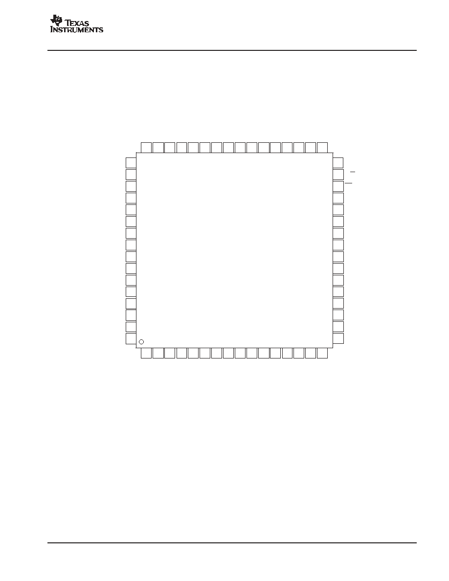
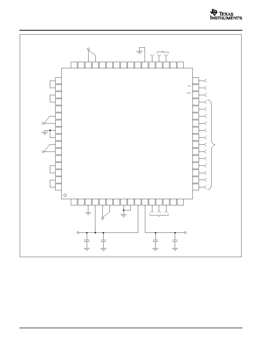
PIN ASSIGNMENTS
LQFP PACKAGE
(TOP VIEW)
32
31
30
29
28
27
26
25
24
23
22
21
20
19
18
17
LDAC
R/W
CS
DB0
DB1
DB2
DB3
DB4
DB5
DB6
DB7
DB8
DB9
DB10
DB11
DB12
49
50
51
52
53
54
55
56
57
58
59
60
61
62
63
64
NC
NC
V
OU
T
D
V
OU
T
DS
e
n
s
e
1
V
OU
T
DS
e
n
s
e
2
NC
NC
NC
NC
NC
RS
T
S
E
L
RS
T
A0
A1
NC
NC
NC
NC
V
SS
V
CC
V
OU
T
A
V
OU
T
A
S
ens
e
1
V
OU
T
A
S
ens
e
2
AG
N
D
DG
ND
V
DD
IO
V
DD
DB
1
5
DB
1
4
DB
1
3
NC
NC
48
47
46
45
44
43
42
41
40
39
38
1
2
3
4
5
6
7
8
9
10
11
37
36
35
34
33
12
13
14
15
16
DAC7664
Offset D Range 1
Offset D Range 2
Offset C Range 2
Offset C Range 1
V
OUT
C Sense 2
V
OUT
C Sense 1
V
OUT
C
REF GND
REF GND
V
OUT
B
V
OUT
B Sense 1
V
OUT
B Sense 2
Offset B Range 1
Offset B Range 2
Offset A Range 2
Offset A Range 1
DAC7664
SBAS271 - MARCH 2004
www.ti.com
6
Terminal Functions
PIN
NAME
DESCRIPTION
1
NC
No Connection
2
NC
No Connection
3
VSS
Analog ≠5V power supply or 0V single supply
4
VCC
Analog +5V power supply
5
VOUTA
DAC A output voltage
6
VOUTA
Sense 1
Connect to VOUTA for unipolar mode
7
VOUTA
Sense 2
Connect to VOUTA for bipolar mode
8
AGND
Analog ground
9
DGND
Digital ground
10
VDD
Digital +5V power supply
11
IOVDD
Interface power supply
12
DB15
Data bit 15 (MSB)
13
DB14
Data bit 14
14
DB13
Data bit 13
15
NC
No connection
16
NC
No connection
17
DB12
Data bit 12
18
DB11
Data bit 11
19
DB10
Data bit 10
20
DB9
Data bit 9
21
DB8
Data bit 8
22
DB7
Data bit 7
23
DB6
Data bit 6
24
DB5
Data bit 5
25
DB4
Data bit 4
26
DB3
Data bit 3
27
DB2
Data bit 2
28
DB1
Data bit 1
29
DB0
Data bit 0
30
CS
Chip select, active low
31
R/W
Enabled by CS; controls the data read and
data write.
32
LDAC
DAC register load control, rising edge
triggered.
33
NC
No connection
34
NC
No connection
35
A1
Enabled by CS; in combination with A0,
selects the individual DAC input registers.
36
A0
Enabled by CS; in combination with A1,
selects the individual DAC input registers.
37
RST
Reset, rising edge triggered. Depending on
the state of RSTSEL, the DAC registers are
set to either mid-scale or zero.
PIN
NAME
DESCRIPTION
38
RSTSEL
Reset select. Determines the action of RST.
If high, an RST command sets the DAC
registers to mid-scale (8000h). If low, an RST
command sets the DAC registers to zero
(0000h).
39
NC
No connection
40
NC
No connection
41
NC
No connection
42
NC
No connection
43
NC
No connection
44
VOUTD
Sense 2
Connect to VOUTD for bipolar mode
45
VOUTD
Sense 1
Connect to VOUTD for unipolar mode
46
VOUTD
DAC D output
47
NC
No connection
48
NC
No connection
49
Offset D
Range 1
Connect to Offset D Range 2 for unipolar
mode
50
Offset D
Range 2
Connect to Offset D Range 1 for unipolar
mode
51
Offset C
Range 2
Connect to Offset C Range 1 for unipolar
mode
52
Offset C
Range 1
Connect to Offset C Range 2 for unipolar
mode
53
VOUTC
Sense 2
Connect to VOUTC for bipolar mode
54
VOUTC
Sense 1
Connect to VOUTC for unipolar mode
55
VOUTC
DAC C output
56
REF GND
Reference ground
57
REF GND
Reference ground
58
VOUTB
DAC B output
59
VOUTB
Sense 1
Connect to VOUTB for unipolar mode
60
VOUTB
Sense 2
Connect to VOUTB for bipolar mode
61
Offset B
Range 1
Connect to Offset B Range 2 for unipolar
mode
62
Offset B
Range 2
Connect to Offset B Range 1 for unipolar
mode
63
Offset A
Range 2
Connect to Offset A Range 1 for unipolar
mode
64
Offset A
Range 1
Connect to Offset A Range 2 for unipolar
mode

DAC7664
SBAS271 - MARCH 2004
www.ti.com
7
TYPICAL CHARACTERISTICS: V
SS
= 0V (+25
∞
C)
All specifications at TA = 25
∞
C, IOVDD = VDD = VCC = +5V, VSS = 0V, representative unit, unless otherwise noted.
Figure 1
2.0
1.5
1.0
0.5
0
-
0.5
-
1.0
-
1.5
-
2.0
2.0
1.5
1.0
0.5
0
-
0.5
-
1.0
-
1.5
-
2.0
LE
(
L
S
B
)
DL
E
(
L
S
B
)
LINEARITY ERROR AND
DIFFERENTIAL LINEARITY ERROR vs CODE
(DAC A, +25
_
C)
0000h 2000h
4000h
6000h
8000h
Digital Input Code
A000h C000h E000h FFFFh
Figure 2
LINEARITY ERROR AND
DIFFERENTIAL LINEARITY ERROR vs CODE
(DAC B, +25
_
C)
2.0
1.5
1.0
0.5
0
-
0.5
-
1.0
-
1.5
-
2.0
2.0
1.5
1.0
0.5
0
-
0.5
-
1.0
-
1.5
-
2.0
L
E
(
L
SB)
DL
E
(
L
S
B
)
0000h 2000h 4000h
6000h
8000h
Digital Input Code
A000h C000h E000h FFFFh
Figure 3
LINEARITY ERROR AND
DIFFERENTIAL LINEARITY ERROR vs CODE
(DAC C, +25
_
C)
2.0
1.5
1.0
0.5
0
-
0.5
-
1.0
-
1.5
-
2.0
2.0
1.5
1.0
0.5
0
-
0.5
-
1.0
-
1.5
-
2.0
L
E
(
L
SB)
D
L
E
(
L
SB)
0000h 2000h 4000h
6000h
8000h
Digital Input Code
A000h C000h E000h FFFFh
Figure 4
LINEARITY ERROR AND
DIFFERENTIAL LINEARITY ERROR vs CODE
(DAC D, +25
_
C)
2.0
1.5
1.0
0.5
0
-
0.5
-
1.0
-
1.5
-
2.0
2.0
1.5
1.0
0.5
0
-
0.5
-
1.0
-
1.5
-
2.0
L
E
(
L
SB)
D
L
E
(
L
SB)
0000h 2000h
4000h
6000h
8000h
Digital Input Code
A000h C000h E000h FFFFh
DAC7664
SBAS271 - MARCH 2004
www.ti.com
8
TYPICAL CHARACTERISTICS: V
SS
= 0V (+85
∞
C)
All specifications at TA = 25
∞
C, IOVDD = VDD = VCC = +5V, VSS = 0V, representative unit, unless otherwise noted.
Figure 5
LINEARITY ERROR AND
DIFFERENTIAL LINEARITY ERROR vs CODE
(DAC A, +85
_
C)
2.0
1.5
1.0
0.5
0
-
0.5
-
1.0
-
1.5
-
2.0
2.0
1.5
1.0
0.5
0
-
0.5
-
1.0
-
1.5
-
2.0
L
E
(
L
SB)
DL
E
(
L
S
B
)
0000h 2000h 4000h
6000h
8000h
Digital Input Code
A000h C000h E000h FFFFh
Figure 6
LINEARITY ERROR AND
DIFFERENTIAL LINEARITY ERROR vs CODE
(DAC B, +85
_
C)
2.0
1.5
1.0
0.5
0
-
0.5
-
1.0
-
1.5
-
2.0
2.0
1.5
1.0
0.5
0
-
0.5
-
1.0
-
1.5
-
2.0
L
E
(
L
SB)
DL
E
(
L
S
B
)
0000h 2000h 4000h
6000h
8000h
Digital Input Code
A000h C000h E000h FFFFh
Figure 7
LINEARITY ERROR AND
DIFFERENTIAL LINEARITY ERROR vs CODE
(DAC C, +85
_
C)
2.0
1.5
1.0
0.5
0
-
0.5
-
1.0
-
1.5
-
2.0
2.0
1.5
1.0
0.5
0
-
0.5
-
1.0
-
1.5
-
2.0
LE
(
L
S
B
)
D
L
E
(
L
SB)
0000h 2000h 4000h
6000h
8000h
Digital Input Code
A000h C000h E000h FFFFh
Figure 8
LINEARITY ERROR AND
DIFFERENTIAL LINEARITY ERROR vs CODE
(DAC D, +85
_
C)
2.0
1.5
1.0
0.5
0
-
0.5
-
1.0
-
1.5
-
2.0
2.0
1.5
1.0
0.5
0
-
0.5
-
1.0
-
1.5
-
2.0
LE
(
L
S
B
)
DL
E
(
L
S
B
)
0000h 2000h
4000h
6000h
8000h
Digital Input Code
A000h C000h E000h FFFFh
DAC7664
SBAS271 - MARCH 2004
www.ti.com
9
TYPICAL CHARACTERISTICS: V
SS
= 0V (-40
∞
C)
All specifications at TA = 25
∞
C, IOVDD = VDD = VCC = +5V, VSS = 0V, representative unit, unless otherwise noted.
Figure 9
LINEARITY ERROR AND
DIFFERENTIAL LINEARITY ERROR vs CODE
(DAC A,
-
40
_
C)
2.0
1.5
1.0
0.5
0
-
0.5
-
1.0
-
1.5
-
2.0
2.0
1.5
1.0
0.5
0
-
0.5
-
1.0
-
1.5
-
2.0
LE
(
L
S
B
)
DL
E
(
L
S
B
)
0000h 2000h 4000h
6000h
8000h
Digital Input Code
A000h C000h E000h FFFFh
Figure 10
LINEARITY ERROR AND
DIFFERENTIAL LINEARITY ERROR vs CODE
(DAC B,
-
40
_
C)
2.0
1.5
1.0
0.5
0
-
0.5
-
1.0
-
1.5
-
2.0
2.0
1.5
1.0
0.5
0
-
0.5
-
1.0
-
1.5
-
2.0
LE
(
L
S
B
)
DL
E
(
L
S
B
)
0000h 2000h
4000h
6000h
8000h
Digital Input Code
A000h C000h E000h FFFFh
Figure 11
LINEARITY ERROR AND
DIFFERENTIAL LINEARITY ERROR vs CODE
(DAC C,
-
40
_
C)
2.0
1.5
1.0
0.5
0
-
0.5
-
1.0
-
1.5
-
2.0
2.0
1.5
1.0
0.5
0
-
0.5
-
1.0
-
1.5
-
2.0
L
E
(
L
SB)
DL
E
(
L
S
B
)
0000h 2000h 4000h
6000h
8000h
Digital Input Code
A000h C000h E000h FFFFh
Figure 12
LINEARITY ERROR AND
DIFFERENTIAL LINEARITY ERROR vs CODE
(DAC D,
-
40
_
C)
2.0
1.5
1.0
0.5
0
-
0.5
-
1.0
-
1.5
-
2.0
2.0
1.5
1.0
0.5
0
-
0.5
-
1.0
-
1.5
-
2.0
LE
(
L
S
B
)
DL
E
(
L
S
B
)
0000h 2000h
4000h
6000h
8000h
Digital Input Code
A000h C000h E000h FFFFh
DAC7664
SBAS271 - MARCH 2004
www.ti.com
10
TYPICAL CHARACTERISTICS: V
SS
= 0V
All specifications at TA = 25
∞
C, IOVDD = VDD = VCC = +5V, VSS = 0V, representative unit, unless otherwise noted.
Figure 13
5.0
4.5
4.0
3.5
3.0
2.5
2.0
1.5
1.0
0.5
0
I
CC
(m
A
)
-
40
-
15
10
35
60
85
Temperature (
_
C)
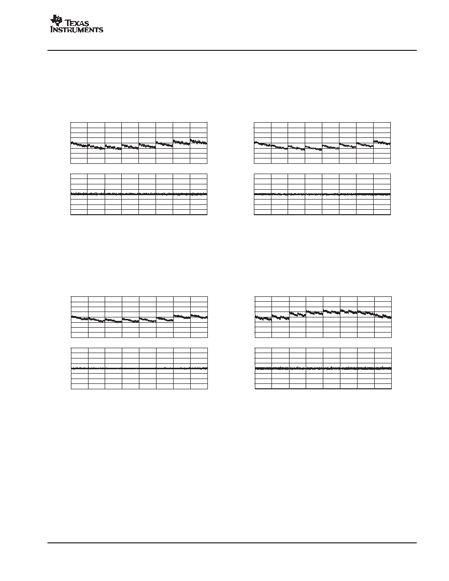
SUPPLY CURRENT vs TEMPERATURE
All DACs at Midscale
No Load
I
CC
Figure 14
5.0
4.5
4.0
3.5
3.0
2.5
2.0
1.5
1.0
0.5
0
Digital Input Code
0000h
2000h 4000h
6000h
8000h
A000h C000h
E000h FFFFh
SUPPLY CURRENT vs DIGITAL INPUT CODE
I
CC
(m
A
)
All DACs
No Load
I
CC
Figure 15
10
8
6
4
2
0
-
2
-
4
-
6
-
8
-
10
Ze
ro
-
S
c
a
l
e
E
rr
o
r
(m
V
)
-
40
-
15
10
35
60
85
Temperature (
_
C)
ZERO-SCALE ERROR vs TEMPERATURE
DAC A
DAC C
DAC B
DAC D
(Code 0000h)
Figure 16
10
8
6
4
2
0
-
2
-
4
-
6
-
8
-
10
P
o
s
i
t
i
ve
F
u
l
l
-
S
ca
l
e
E
r
r
o
r
(
m
V
)
-
40
-
15
10
35
60
85
Temperature (
_
C)
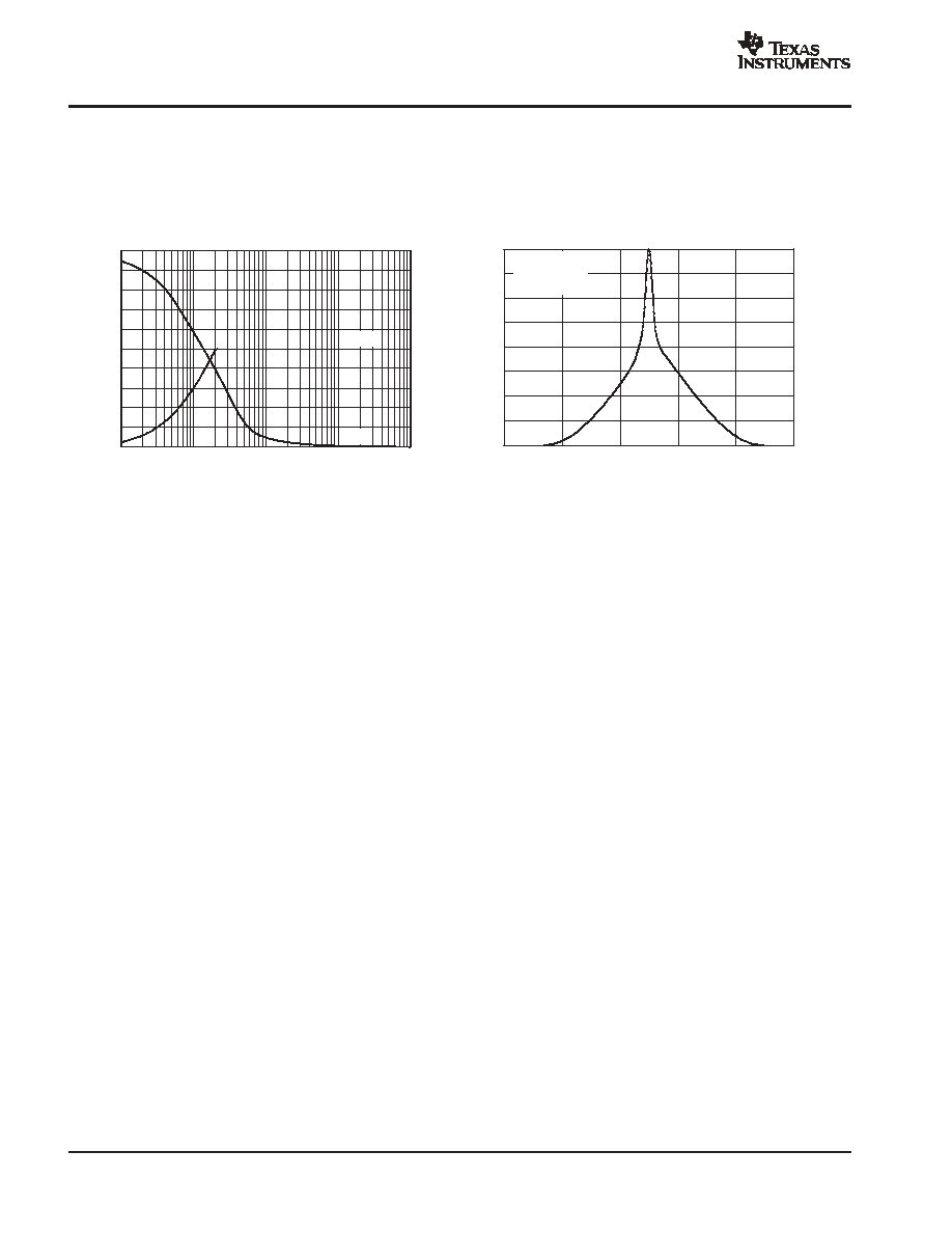
POSITIVE FULL-SCALE ERROR vs TEMPERATURE
DAC C
DAC B
DAC D
DAC A
(Code FFFFh)
N
o
i
s
e
V
ol
t
age
(
1
0
0
µ
V/
d
i
v
)
Time (10ms/div)
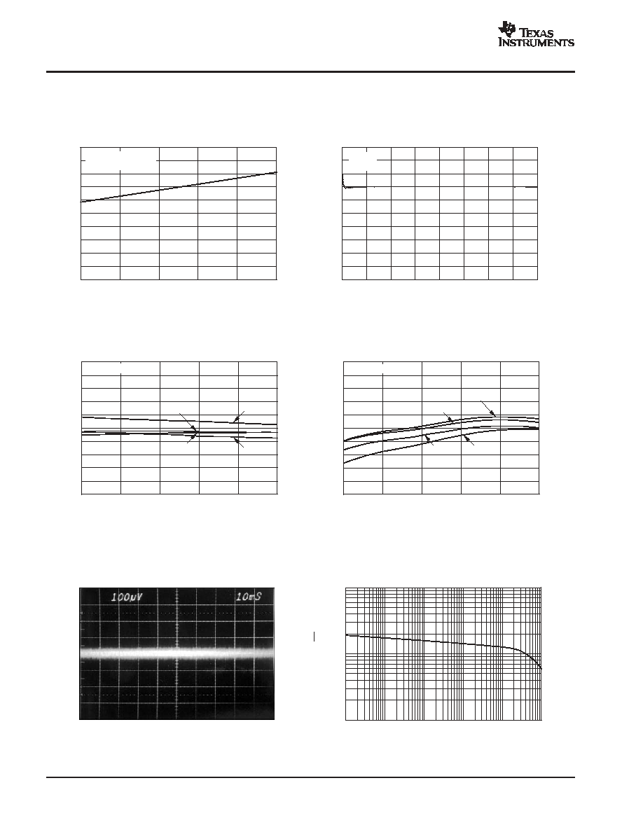
BROADBAND NOISE
(Code = 8000h, BW = 10kHz)
Figure 17
Figure 18
1000
100
10
No
i
s
e
(
n
V
Hz
)
10
100
1k
10k
100k
1M
Frequency (Hz)
OUTPUT NOISE VOLTAGE vs FREQUENCY
DAC7664
SBAS271 - MARCH 2004
www.ti.com
11
TYPICAL CHARACTERISTICS: V
SS
= 0V (continued)
All specifications at TA = 25
∞
C, IOVDD = VDD = VCC = +5V, VSS = 0V, representative unit, unless otherwise noted.
Figure 19
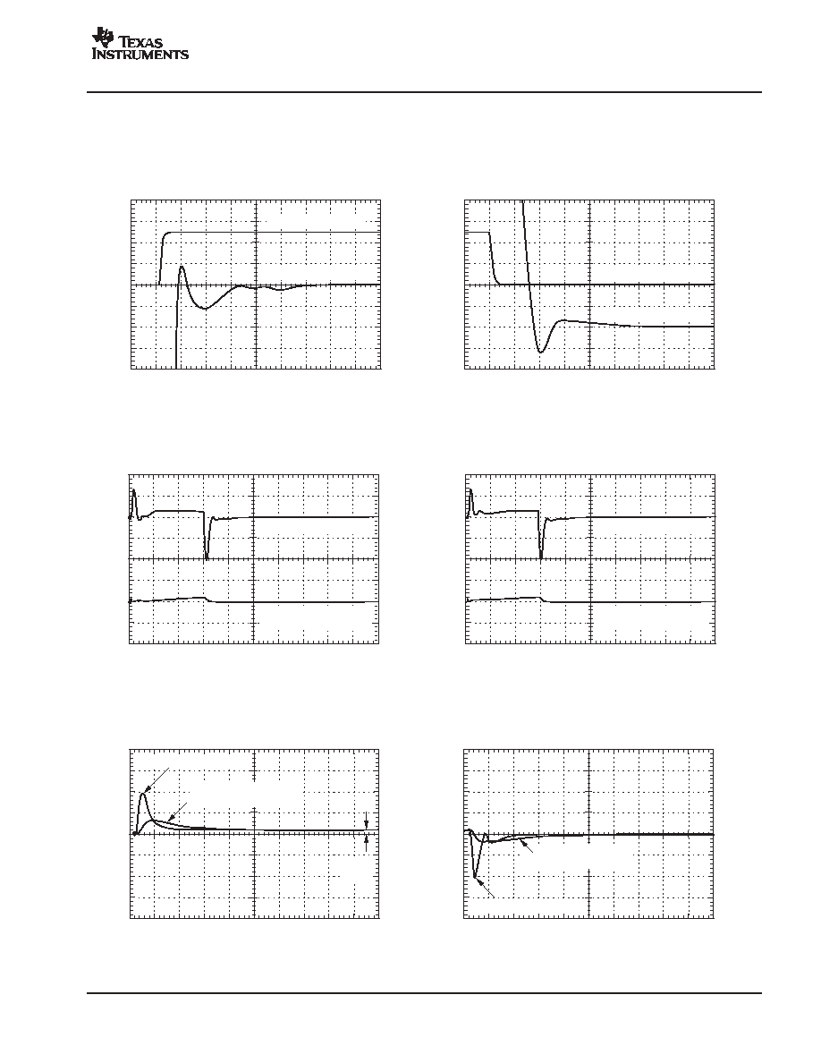
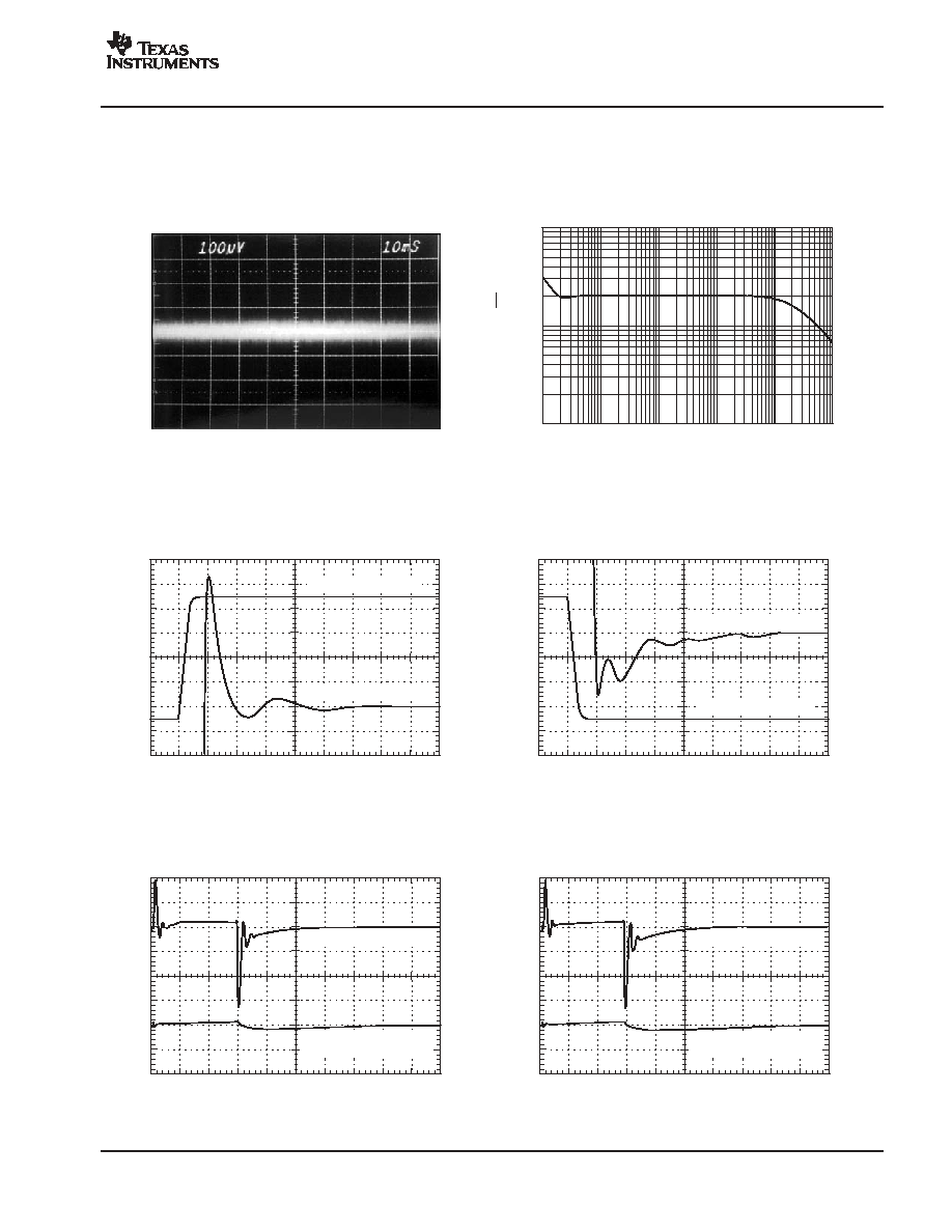
SETTLING TIME
(0V to +2.5V)
Time (5
µ
s/div)
O
u
tput
V
o
l
t
ag
e
Large Signal: 1.0V/div
Small Signal: 100
µ
V/div
Figure 20
SETTLING TIME
(+2.5V to 39mV)
Time (5
µ
s/div)
O
u
tput
V
o
l
t
ag
e
Large Signal: 1.0V/div
Small Signal: 100
µ
V/div
Figure 21
MIDSCALE GLITCH PERFORMANCE
CODE 7FFFh to 8000h
Time (0.5
µ
s/div)
O
u
t
p
ut
V
o
l
t
ag
e
(
1
0
m
V
/
di
v
)
Unfiltered DAC Output
DAC Output after
2K, 470pF Low-Pass Filter
Figure 22
MIDSCALE GLITCH PERFORMANCE
CODE 8000h to 7FFFh
Time (0.5
µ
s/div)
O
u
t
p
ut
V
o
l
t
ag
e
(
1
0
m
V
/
di
v
)
Unfiltered DAC Output
DAC Output After
2K, 470pF Low-Pass Filter
Figure 23
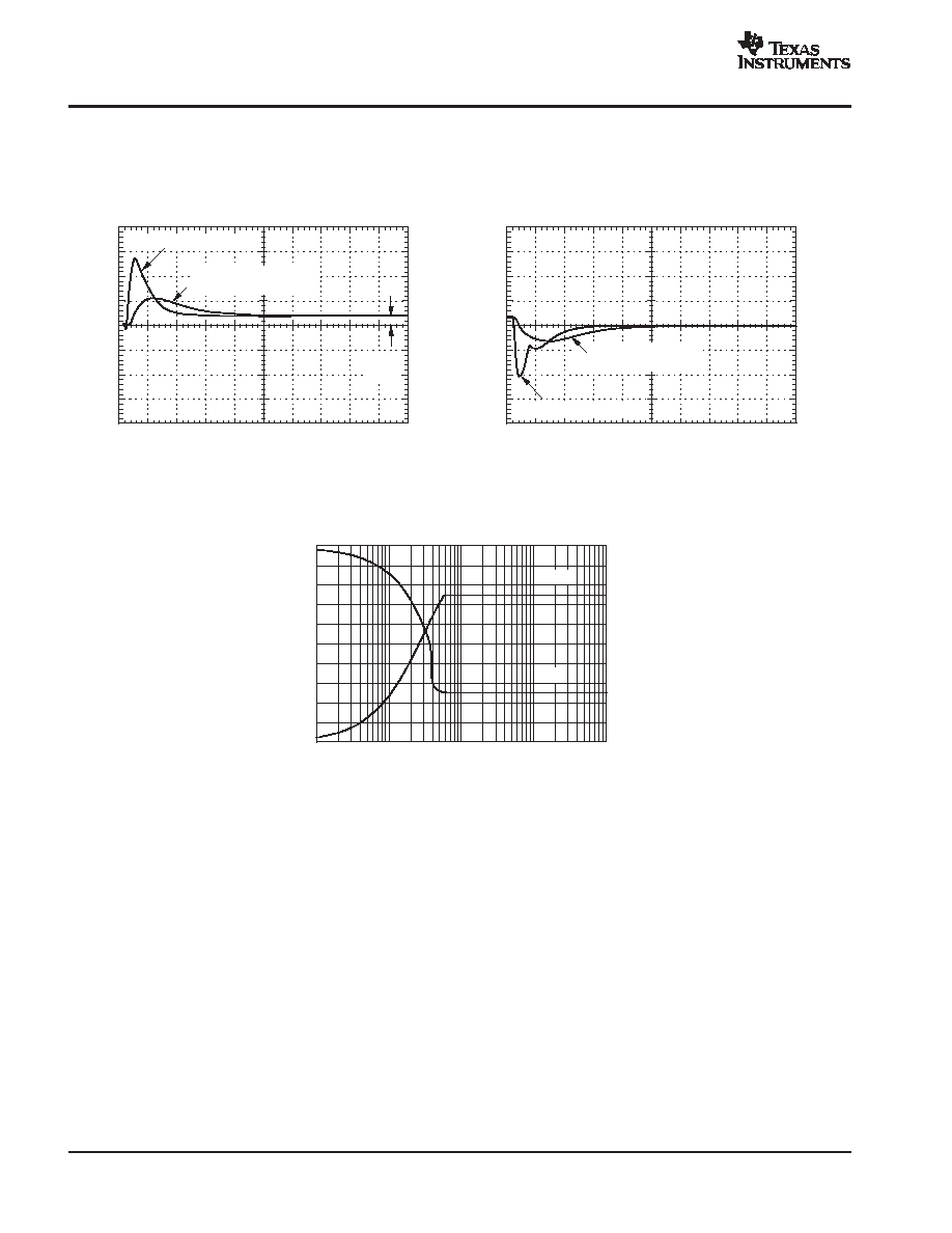
OVERSHOOT FOR TRANSITION OF 100 CODES
CODE 32750 to 32850
Time (1.0
µ
s/div)
O
u
t
p
ut
V
o
l
t
ag
e
(
2
0
m
V
/
di
v
)
Unfiltered DAC Output
100
Codes
DAC Output After
2K, 470pF Low-Pass Filter
Figure 24
OVERSHOOT FOR TRANSITION OF 100 CODES
CODE 32850 to 32750
Time (1.0
µ
s/div)
O
u
t
p
ut
V
o
l
t
ag
e
(
2
0
m
V
/
di
v
)
Unfiltered DAC Output
DAC Output After
2K, 470pF Low-Pass Filter
DAC7664
SBAS271 - MARCH 2004
www.ti.com
12
TYPICAL CHARACTERISTICS: V
SS
= 0V (continued)
All specifications at TA = 25
∞
C, IOVDD = VDD = VCC = +5V, VSS = 0V, representative unit, unless otherwise noted.
Figure 25
5.0
4.5
4.0
3.5
3.0
2.5
2.0
1.5
1.0
0.5
0
V
OU
T
(V
)
0.01
0.1
1
10
100
R
LOAD
(k
)
V
OUT
vs R
LOAD
Sink
Source
Figure 26
0.8
0.7
0.6
0.5
0.4
0.3
0.2
0.1
0
Log
i
c
S
u
p
p
l
y
C
u
r
r
ent
(
m
A
)
0
1
2
3
4
5
Logic Input Level for Digital Inputs (V)
IOVDD SUPPLY CURRENT
vs LOGIC INPUT LEVEL FOR DIGITAL INPUTS
Typical of One
Digital Input
IOVDD = 5V
DAC7664
SBAS271 - MARCH 2004
www.ti.com
13
TYPICAL CHARACTERISTICS: V
SS
= -5V (+25
∞
C)
All specifications at TA = 25
∞
C, IOVDD = VDD = VCC = +5V, VSS = -5V, representative unit, unless otherwise noted.
Figure 27
2.0
1.5
1.0
0.5
0
-
0.5
-
1.0
-
1.5
-
2.0
2.0
1.5
1.0
0.5
0
-
0.5
-
1.0
-
1.5
-
2.0
LE
(
L
S
B
)
DL
E
(
L
S
B
)
LINEARITY ERROR AND
DIFFERENTIAL LINEARITY ERROR vs CODE
(DAC A, +25
_
C)
0000h 2000h
4000h
6000h
8000h
Digital Input Code
A000h C000h E000h FFFFh
Figure 28
LINEARITY ERROR AND
DIFFERENTIAL LINEARITY ERROR vs CODE
(DAC B, +25
_
C)
2.0
1.5
1.0
0.5
0
-
0.5
-
1.0
-
1.5
-
2.0
2.0
1.5
1.0
0.5
0
-
0.5
-
1.0
-
1.5
-
2.0
LE
(
L
S
B
)
D
L
E
(
L
SB)
0000h 2000h 4000h
6000h
8000h
Digital Input Code
A000h C000h E000h FFFFh
Figure 29
LINEARITY ERROR AND
DIFFERENTIAL LINEARITY ERROR vs CODE
(DAC C, +25
_
C)
2.0
1.5
1.0
0.5
0
-
0.5
-
1.0
-
1.5
-
2.0
2.0
1.5
1.0
0.5
0
-
0.5
-
1.0
-
1.5
-
2.0
LE
(
L
S
B
)
DL
E
(
L
S
B
)
0000h 2000h
4000h
6000h
8000h
Digital Input Code
A000h C000h E000h FFFFh
Figure 30
LINEARITY ERROR AND
DIFFERENTIAL LINEARITY ERROR vs CODE
(DAC D, +25
_
C)
2.0
1.5
1.0
0.5
0
-
0.5
-
1.0
-
1.5
-
2.0
2.0
1.5
1.0
0.5
0
-
0.5
-
1.0
-
1.5
-
2.0
LE
(
L
S
B
)
D
L
E
(
L
SB)
0000h 2000h
4000h
6000h
8000h
Digital Input Code
A000h C000h E000h FFFFh
DAC7664
SBAS271 - MARCH 2004
www.ti.com
14
TYPICAL CHARACTERISTICS: V
SS
= -5V (+85
∞
C)
All specifications at TA = 25
∞
C, IOVDD = VDD = VCC = +5V, VSS = -5V, representative unit, unless otherwise noted.
Figure 31
2.0
1.5
1.0
0.5
0
-
0.5
-
1.0
-
1.5
-
2.0
2.0
1.5
1.0
0.5
0
-
0.5
-
1.0
-
1.5
-
2.0
LE
(
L
S
B
)
DL
E
(
L
S
B
)
LINEARITY ERROR AND
DIFFERENTIAL LINEARITY ERROR vs CODE
(DAC A, +85
_
C)
0000h 2000h
4000h
6000h
8000h
Digital Input Code
A000h C000h E000h FFFFh
Figure 32
2.0
1.5
1.0
0.5
0
-
0.5
-
1.0
-
1.5
-
2.0
2.0
1.5
1.0
0.5
0
-
0.5
-
1.0
-
1.5
-
2.0
LE
(
L
S
B
)
DL
E
(
L
S
B
)
LINEARITY ERROR AND
DIFFERENTIAL LINEARITY ERROR vs CODE
(DAC B, +85
_
C)
0000h 2000h
4000h
6000h
8000h
Digital Input Code
A000h C000h E000h FFFFh
Figure 33
2.0
1.5
1.0
0.5
0
-
0.5
-
1.0
-
1.5
-
2.0
2.0
1.5
1.0
0.5
0
-
0.5
-
1.0
-
1.5
-
2.0
LE
(
L
S
B
)
DL
E
(
L
S
B
)
LINEARITY ERROR AND
DIFFERENTIAL LINEARITY ERROR vs CODE
(DAC C, +85
_
C)
0000h 2000h
4000h
6000h
8000h
Digital Input Code
A000h C000h E000h FFFFh
Figure 34
2.0
1.5
1.0
0.5
0
-
0.5
-
1.0
-
1.5
-
2.0
2.0
1.5
1.0
0.5
0
-
0.5
-
1.0
-
1.5
-
2.0
LE
(
L
S
B
)
DL
E
(
L
S
B
)
LINEARITY ERROR AND
DIFFERENTIAL LINEARITY ERROR vs CODE
(DAC D, +85
_
C)
0000h 2000h 4000h
6000h
8000h
Digital Input Code
A000h C000h E000h FFFFh

DAC7664
SBAS271 - MARCH 2004
www.ti.com
15
TYPICAL CHARACTERISTICS: V
SS
= -5V (-40
∞
C)
All specifications at TA = 25
∞
C, IOVDD = VDD = VCC = +5V, VSS = -5V, representative unit, unless otherwise noted.
Figure 35
2.0
1.5
1.0
0.5
0
-
0.5
-
1.0
-
1.5
-
2.0
2.0
1.5
1.0
0.5
0
-
0.5
-
1.0
-
1.5
-
2.0
LE
(
L
S
B
)
DL
E
(
L
S
B
)
LINEARITY ERROR AND
DIFFERENTIAL LINEARITY ERROR vs CODE
(DAC A,
-
40
_
C)
0000h 2000h
4000h
6000h
8000h
Digital Input Code
A000h C000h E000h FFFFh
Figure 36
2.0
1.5
1.0
0.5
0
-
0.5
-
1.0
-
1.5
-
2.0
2.0
1.5
1.0
0.5
0
-
0.5
-
1.0
-
1.5
-
2.0
LE
(
L
S
B
)
DL
E
(
L
S
B
)
LINEARITY ERROR AND
DIFFERENTIAL LINEARITY ERROR vs CODE
(DAC B,
-
40
_
C)
0000h 2000h
4000h
6000h
8000h
Digital Input Code
A000h C000h E000h FFFFh
Figure 37
2.0
1.5
1.0
0.5
0
-
0.5
-
1.0
-
1.5
-
2.0
2.0
1.5
1.0
0.5
0
-
0.5
-
1.0
-
1.5
-
2.0
LE
(
L
S
B
)
DL
E
(
L
S
B
)
LINEARITY ERROR AND
DIFFERENTIAL LINEARITY ERROR vs CODE
(DAC C,
-
40
_
C)
0000h 2000h 4000h
6000h
8000h
Digital Input Code
A000h C000h E000h FFFFh
Figure 38
2.0
1.5
1.0
0.5
0
-
0.5
-
1.0
-
1.5
-
2.0
2.0
1.5
1.0
0.5
0
-
0.5
-
1.0
-
1.5
-
2.0
LE
(
L
S
B
)
DL
E
(
L
S
B
)
LINEARITY ERROR AND
DIFFERENTIAL LINEARITY ERROR vs CODE
(DAC D,
-
40
_
C)
0000h 2000h
4000h
6000h
8000h
Digital Input Code
A000h C000h E000h FFFFh

DAC7664
SBAS271 - MARCH 2004
www.ti.com
16
TYPICAL CHARACTERISTICS: V
SS
= -5V
All specifications at TA = 25
∞
C, IOVDD = VDD = VCC = +5V, VSS = -5V, representative unit, unless otherwise noted.
Figure 39
5
4
3
2
1
0
-
1
-
2
-
3
-
4
-
5
I
CC
(m
A
)
-
40
-
15
10
35
60
85
Temperature (
_
C)
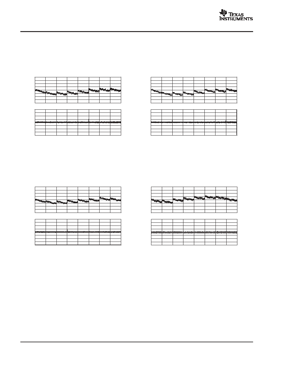
SUPPLY CURRENT vs TEMPERATURE
All DACs at Midscale
No Load
I
CC
I
SS
Figure 40
5
4
3
2
1
0
-
1
-
2
-
3
-
4
-
5
Digital Input Code
0000h
2000h 4000h 6000h
8000h
A000h C000h
E000h FFFFh
SUPPLY CURRENT vs DIGITAL INPUT CODE
I
CC
(m
A
)
All DACs
No Load
I
CC
I
SS
Figure 41
10
8
6
4
2
0
-
2
-
4
-
6
-
8
-
10
B
i
po
l
a
r
Z
er
o
E
r
r
or
(
m
V
)
-
40
-
15
10
35
60
85
Temperature (
_
C)
BIP L
O AR ZERO ERROR vs TEMPERATURE
DAC B
DAC C
DAC D
DAC A
(Code 8000h)
Figure 42
10
8
6
4
2
0
-
2
-
4
-
6
-
8
-
10
P
o
s
i
t
i
ve
F
u
l
l
-
S
ca
l
e
E
r
r
o
r
(
m
V
)
-
40
-
15
10
35
60
85
Temperature (
_
C)
POSITIVE FULL- SCALE ERROR vs TEMPERATURE
DAC B
DAC C
DAC D
DAC A
(Code FFFFh)
Figure 43
10
8
6
4
2
0
-
2
-
4
-
6
-
8
-
10
Ne
g
a
ti
v
e
F
u
l
l
-
S
c
a
l
e
E
r
r
o
r
(
m
V
)
-
40
-
15
10
35
60
85
Temperature (
_
C)
NEGATIVE FULL- SCALE ERROR vs TEMPERATURE
DAC B
DAC C
DAC D
DAC A
(Code 0000h)
DAC7664
SBAS271 - MARCH 2004
www.ti.com
17
TYPICAL CHARACTERISTICS: V
SS
= -5V (continued)
All specifications at TA = 25
∞
C, IOVDD = VDD = VCC = +5V, VSS = -5V, representative unit, unless otherwise noted.
Figure 44
N
o
i
s
e
V
ol
ta
g
e
(
100
µ
V/
d
i
v)
Time (10ms/div)
BROADBAND NOISE
(Code = 8000h, BW = 10kHz)
Figure 45
1000
100
10
No
i
s
e
(
n
V
Hz
)
10
100
1k
10k
100k
1M
Frequency (Hz)
OUTPUT NOISE VOLTAGE vs FREQUENCY
Figure 46
SETTLING TIME
(
-
2.5V to +2.5V)
Time (5
µ
s/div)
O
u
tput
V
o
l
t
ag
e
Large Signal: 1.0V/div
Small Signal: 100
µ
V/div
Figure 47
SETTLING TIME
(+2.5V to
-
2.5V)
Time (5
µ
s/div)
O
u
tput
V
o
l
t
ag
e
Large Signal: 1.0V/div
Small Signal: 100
µ
V/div
Figure 48
MIDSCALE GLITCH PERFORMANCE
CODE 7FFFh to 8000h
Time (0.5
µ
s/div)
O
u
t
p
ut
V
o
l
t
ag
e
(
1
0
m
V
/
di
v
)
Unfiltered DAC Output
DAC Output after
2K, 470pF Low-Pass Filter
Figure 49
MIDSCALE GLITCH PERFORMANCE
CODE 8000h to 7FFFh
Time (0.5
µ
s/div)
O
u
t
p
ut
V
o
l
t
ag
e
(
1
0
m
V
/
di
v
)
Unfiltered DAC Output
DAC Output After
2K, 470pF Low-Pass Filter
DAC7664
SBAS271 - MARCH 2004
www.ti.com
18
TYPICAL CHARACTERISTICS: V
SS
= -5V (continued)
All specifications at TA = 25
∞
C, IOVDD = VDD = VCC = +5V, VSS = -5V, representative unit, unless otherwise noted.
Figure 50
OVERSHOOT FOR TRANSITION OF 100 CODES
CODE 32750 to 32850
Time (1.0
µ
s/div)
O
u
t
p
ut
V
o
l
t
ag
e
(
2
0
m
V
/
di
v
)
Unfiltered DAC Output
100
Codes
DAC Output After
2K, 470pF Low-Pass Filter
Figure 51
OVERSHOOT FOR TRANSITION OF 100 CODES
CODE 32850 to 32750
Time (1.0
µ
s/div)
O
u
t
p
ut
V
o
l
t
ag
e
(
2
0
m
V
/
di
v
)
Unfiltered DAC Output
DAC Output After
2K, 470pF Low-Pass Filter
Figure 52
5
4
3
2
1
0
-
1
-
2
-
3
-
4
-
5
V
OU
T
(V
)
0.01
0.1
1
10
100
R
LOAD
(k
)
V
OUT
vs R
LOAD
Sink
Source
DAC7664
SBAS271 - MARCH 2004
www.ti.com
19
THEORY OF OPERATION
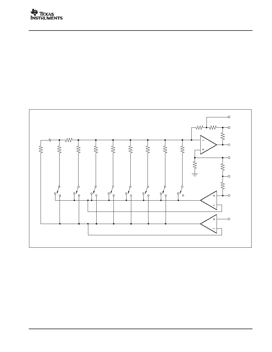
The DAC7664 is a quad voltage output 16-bit DAC. The
architecture is an R-2R ladder configuration with the three
most significant bits (MSBs) segmented, followed by an
operational amplifier that serves as a buffer. Each DAC
has its own R-2R ladder network, segmented MSBs, and
output op amp, as shown in Figure 53. The minimum
voltage output (zero-scale) and maximum voltage output
(full-scale) are set by the internal voltage references and
the resistors associated with the output operational
amplifier.
The digital input is a 16-bit parallel word and the DAC input
registers offer readback capability. The converters can be
powered from either a single +5V supply or a dual
±
5V
supply. The device offers a reset function that immediately
sets all DAC output voltages and DAC registers to
mid-scale (code 8000h) or to zero-scale, code 0000h. See
Figure 54 and Figure 55 for the basic operation of the
DAC7664.
R
2R
2R
2R
2R
2R
2R
2R
2R
2R
V
REF
H
V
REF
L
V
OUT
V
OUT
S2
V
OUT
S1
OFSR2
OFSR1
13K
13K
12K
13K
11K
100
Figure 53. DAC7664 Architecture
DAC7664
SBAS271 - MARCH 2004
www.ti.com
20
0V to +2.5V
32
31
30
29
28
27
26
25
24
23
22
21
20
19
18
17
LDAC
R/W
CS
(LSB) DB0
DB1
DB2
DB3
DB4
DB5
DB6
DB7
DB8
DB9
DB10
DB11
DB12
Load DAC Registers
Read/Write
Chip Select
DAC
Input
Data
49
50
51
52
53
54
55
56
57
58
59
60
61
62
63
64
NC
NC
V
OU
T
D
V
OU
T
DS
e
n
s
e
1
V
OU
T
DS
e
n
s
e
2
NC
NC
NC
NC
NC
RS
T
S
E
L
RS
T
A0
A1
NC
NC
NC
NC
V
SS
V
CC
V
OU
T
A
V
OU
T
AS
e
n
s
e
1
V
OU
T
AS
e
n
s
e
2
AG
N
D
DG
ND
V
DD
IO
V
DD
DB
1
5
(
M
S
B
)
DB
1
4
DB
1
3
NC
NC
48
NC
NC
NC
+5V
+3V to +5V
NC
NC = No Connection
0V to +2.5V
0V to +2.5V
0V to +2.5V
NC
NC NC
NC
NC
NC
NC
NC
NC
NC
NC
NC
RE
S
E
T
DA
C
Se
le
c
t
DAC
Input Data
NC
47
46
45
44
43
42
41
40
39
38
1
2
3
4
5
6
7
8
9
10
11
37
36
35
34
33
12
13
14
15
16
DAC7664
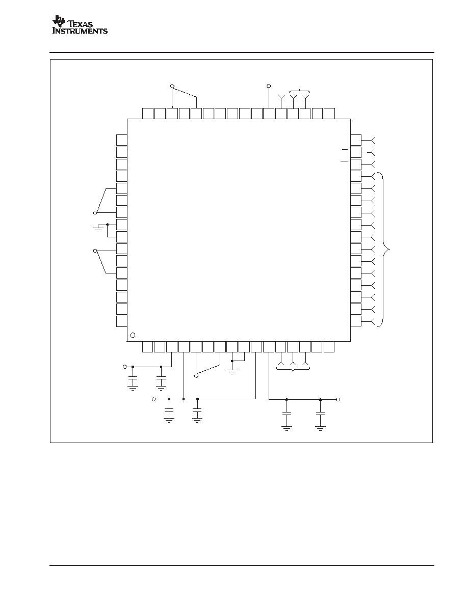
Single Supply
Offset D Range 1
Offset D Range 2
Offset C Range 2
Offset C Range 1
V
OUT
C Sense 2
V
OUT
C Sense 1
V
OUT
C
Reference GND
Reference GND
V
OUT
B
V
OUT
B Sense 1
V
OUT
B Sense 2
Offset B Range 1
Offset B Range 2
Offset A Range 2
Offset A Range 1
0.1
µ
F
0.1
µ
F
1
µ
F
+
1
µ
F
+
Figure 54. Basic Single-Supply Operation of the DAC7664
DAC7664
SBAS271 - MARCH 2004
www.ti.com
21
-
2.5V to +2.5V
+5V
32
31
30
29
28
27
26
25
24
23
22
21
20
19
18
17
NC
NC
NC
NC
NC
NC
NC
NC
NC
NC
49
50
51
52
53
54
55
56
57
58
59
60
61
62
63
64
NC
NC
V
OU
T
D
V
OU
T
DS
e
n
s
e
1
V
OU
T
DS
e
n
s
e
2
NC
NC
NC
NC
NC
RS
T
S
E
L
RS
T
A0
A1
NC
NC
NC
NC
V
SS
V
CC
V
OU
T
A
V
OU
T
AS
e
n
s
e
1
V
OU
T
AS
e
n
s
e
2
AG
N
D
DG
ND
V
DD
IO
V
DD
DB
1
5
(
M
S
B
)
DB
1
4
DB
1
3
NC
NC
48
NC
-
5V
+5V
NC
NC = No Connection
-
2.5V to +2.5V
-
2.5V to +2.5V
-
2.5V to +2.5V
NC
NC NC
NC
NC
NC
NC
NC
NC
NC
NC
NC NC
47
46
45
44
43
42
41
40
39
38
1
2
3
4
5
6
7
8
9
10
11
37
36
35
34
33
12
13
14
15
16
DAC7664
Dual Supply
Offset D Range 1
Offset D Range 2
Offset C Range 2
Offset C Range 1
V
OUT
C Sense 2
V
OUT
C Sense 1
V
OUT
C
Reference GND
Reference GND
V
OUT
B
V
OUT
B Sense 1
V
OUT
B Sense 2
Offset B Range 1
Offset B Range 2
Offset A Range 2
Offset A Range 1
0.1
µ
F
1
µ
F
+
0.1
µ
F
1
µ
F
+
RE
S
E
T
DA
C
Se
l
e
c
t
+3V to +5V
DAC
Input Data
0.1
µ
F
1
µ
F
+
LDAC
R/W
CS
(LSB) DB0
DB1
DB2
DB3
DB4
DB5
DB6
DB7
DB8
DB9
DB10
DB11
DB12
Load DAC Registers
Read/Write
Chip Select
DAC
Input
Data
Figure 55. Basic Dual-Supply Operation of the DAC7664
DAC7664
SBAS271 - MARCH 2004
www.ti.com
22
ANALOG OUTPUTS
When V
SS
= ≠5V (dual-supply operation), the output
amplifier can swing to within 2.25V of the supply rails over
a range of ≠40
∞
C to +85
∞
C. When V
SS
= 0V (single-supply
operation), and with R
LOAD
also connected to ground, the
output can swing to within 5mV of ground. Care must be
taken when measuring the zero-scale error when
V
SS
= 0V. Since the output voltage cannot swing below
ground, the output voltage may not change for the first few
digital input codes (0000h, 0001h, 0002h, etc.) if the output
amplifier has a negative offset.
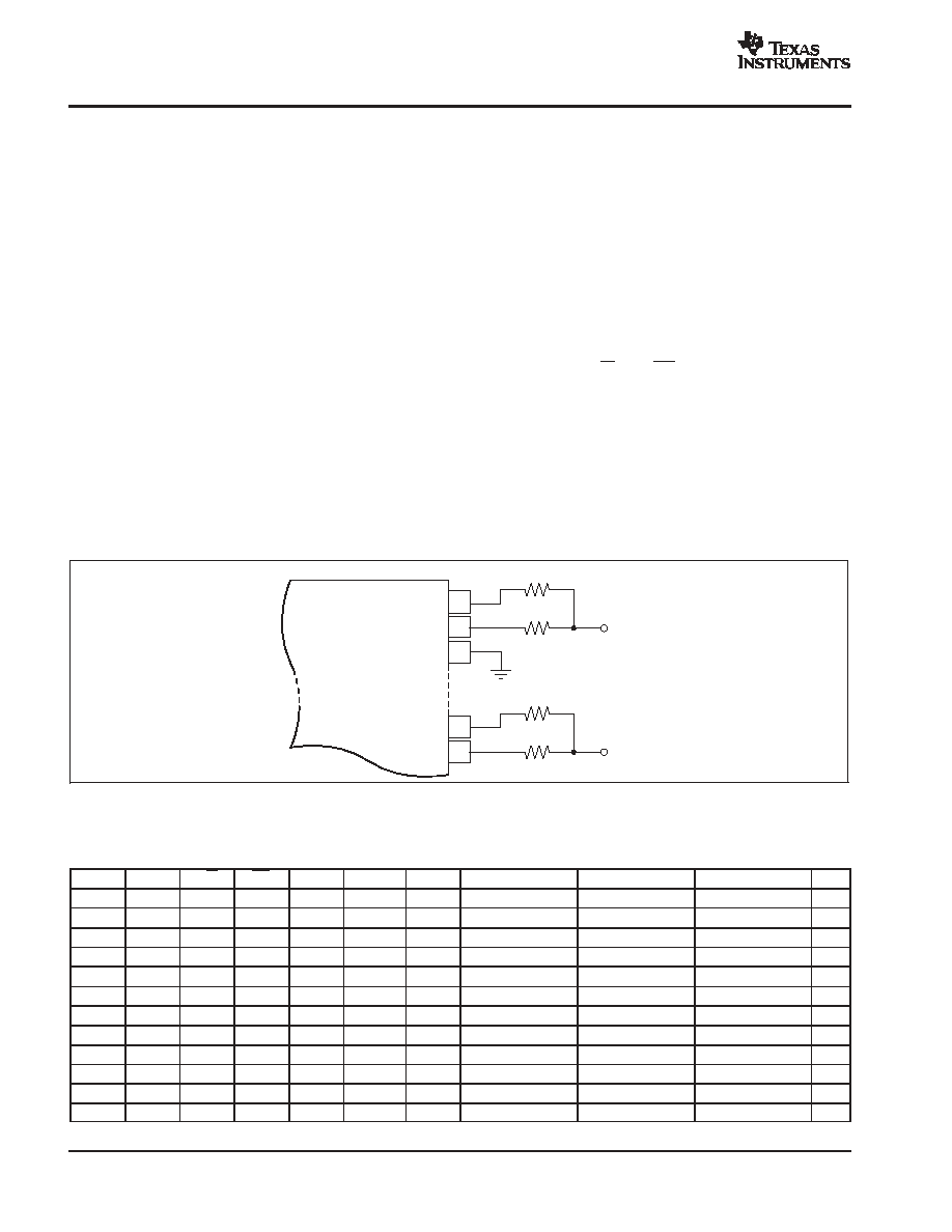
Due to the high accuracy of these DACs, system design
problems such as grounding and contact resistance are
very important. A 16-bit converter with a 2.5V full-scale
range has a 1LSB value of 38
µ
V. With a load current of
1mA, series wiring and connector resistance of only 40m
(R
W2
) will cause a voltage drop of 40
µ
V, as shown in
Figure 56. To understand what this means in terms of
system layout, the resistivity of a typical 1-ounce
copper-clad printed circuit board is 1/2 m
per square. For
a 1mA load, a 0.01-inch-wide printed circuit conductor 0.6
inches long will result in a voltage drop of 30
µ
V.
The DAC7664 offers a force and sense output
configuration for the high open-loop gain output amplifier.
This feature allows the loop around the output amplifier to
be closed at the load (as shown in Figure 56), thus
ensuring an accurate output voltage.
DIGITAL INTERFACE
Table 1 shows the basic control logic for the DAC7664.
Note that each internal register is edge-triggered and not
level-triggered. When the LDAC signal is transitioned to
high, the digital word currently in the register is latched.
The first set of registers (the input registers) are triggered
via the A0, A1, R/W, and CS inputs. Only one of these
registers is transparent at any given time.
The double-buffered architecture is designed mainly so
each DAC input register can be written to at any time and
then all DAC voltages updated simultaneously by the
rising edge of LDAC. It also allows a DAC input register to
be written to at any point and the DAC voltages to be
synchronously changed via a trigger signal connected to
LDAC.
V
OUT
A Sense1
V
OUT
A
AGND
V
OUT
B Sense1
V
OUT
B
6
5
8
59
58
DAC7664
R
W1
R
W2
V
OUT
R
W1
R
W2
V
OUT
Figure 56. Analog Output Closed-Loop Configuration (1/2 DAC7664). R
W
represents wiring resistances.
Table 1. DAC7664 Logic Truth Table
A1
A0
R/W
CS
RST
RSTSEL
LDAC
INPUT REGISTER
DAC REGISTER
MODE
DAC
L
L
L
L
H
X
X
Write
Hold
Write input
A
L
H
L
L
H
X
X
Write
Hold
Write input
B
H
L
L
L
H
X
X
Write
Hold
Write input
C
H
H
L
L
H
X
X
Write
Hold
Write input
D
L
L
H
L
H
X
X
Read
Hold
Read input
A
L
H
H
L
H
X
X
Read
Hold
Read input
B
H
L
H
L
H
X
X
Read
Hold
Read input
C
H
H
H
L
H
X
X
Read
Hold
Read input
D
X
X
X
H
H
X
Hold
Write
Update
All
X
X
X
H
H
X
H
Hold
Hold
Hold
All
X
X
X
X
L
X
Reset to zero
Reset to zero
Reset to zero
All
X
X
X
X
H
X
Reset to mid-scale
Reset to mid-scale
Reset to mid-scale
All

DAC7664
SBAS271 - MARCH 2004
www.ti.com
23
3V TO 5V LOGIC INTERFACE
All of the digital input and output pins are compatible with
any logic supply voltage between 3V and 5V. Connect the
interface logic supply voltage to the IOV
DD
pin. Note that
the internal digital logic operates from 5V, so the VDD pin
must connect to a 5V supply.
GLITCH SUPPRESSION CIRCUIT
Figure 21, Figure 22, Figure 48, and Figure 49 show the
typical DAC output when switching between codes 7FFFh
and 8000h. For R-2R ladder DACs, this is potentially the
worst-case glitch condition, since every switch in the DAC
changes state. To minimize the glitch energy at this and
other code pairs with possible high-glitch outputs, an
internal track-and-hold circuit is used to maintain the DAC
ouput voltage at a nearly constant level during the internal
switching interval. This track-and-hold circuit is activated
only when the transition is at, or close to, one of the code
pairs with the high-glitch possibility.
It is advisable to avoid digital transitions within 1
µ
s of the
rising edge of the LDAC signal. These signals can affect
the charge on the track-and-hold capacitor, thus
increasing the glitch energy.
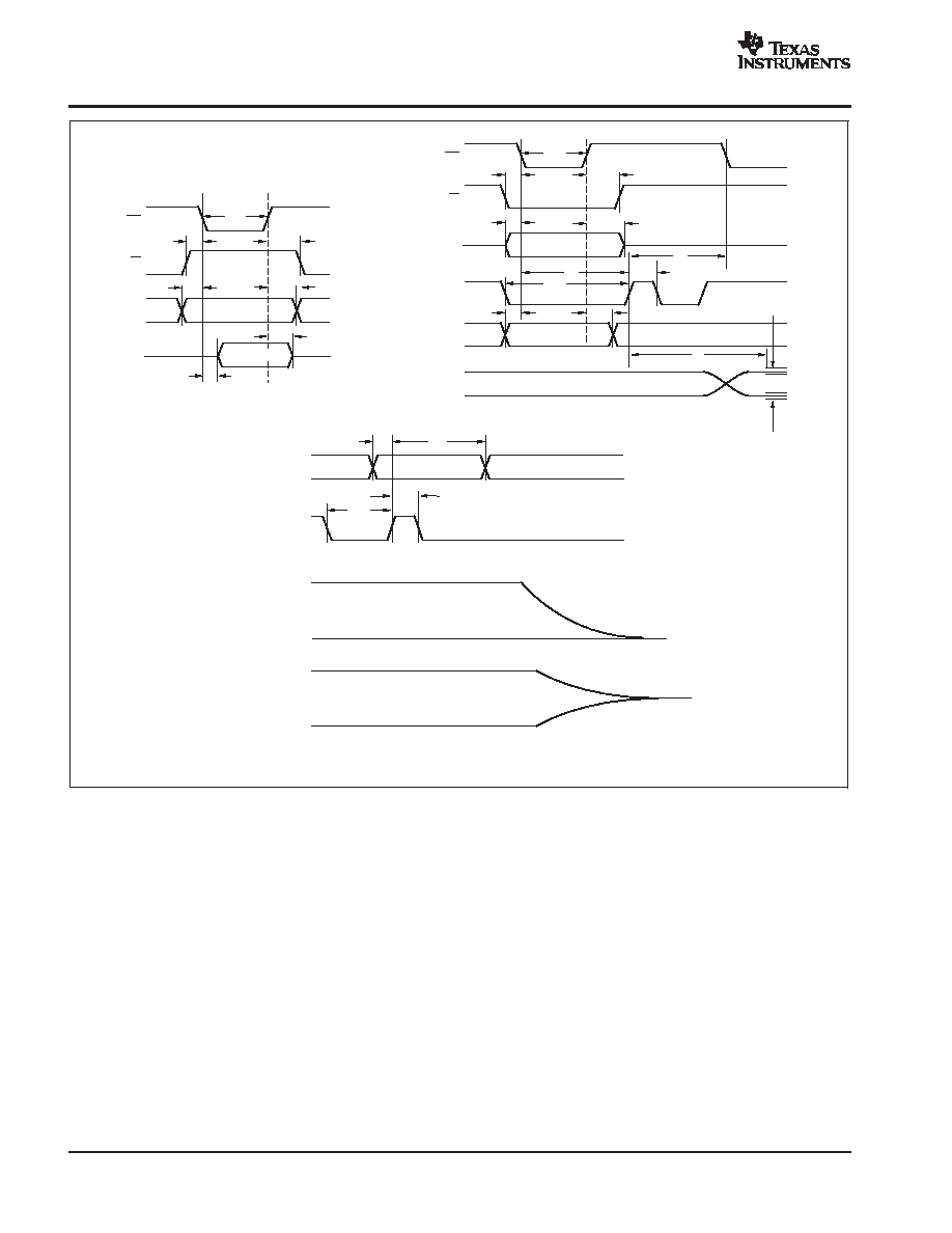
DIGITAL TIMING
Figure 57 and Table 2 provide detailed timing information
for the digital interface of the DAC7664.
DIGITAL INPUT CODING
The DAC7664 input data is in straight binary format. The
output voltage for single-supply operation is given by
Equation 1:
V
OUT
+
2.5
N
65, 536
where N is the digital input code.
This equation does not include the effects of offset
(zero-scale) or gain (full-scale) errors.
The output for the dual supply operation is given by
Equation 2:
V
OUT
+
5
N
65, 536
*
2.5
(1)
(2)
DAC7664
SBAS271 - MARCH 2004
www.ti.com
24
t
RCS
CS
t
RDS
t
RDH
t
AS
t
CSD
t
DZ
t
AH
R/W
A0/A1
Data Out
Data Valid
t
WCS
CS
t
WS
t
AS
t
AH
t
WH
R/W
A0/A1
t
LS
t
LWD
t
LH
t
S
±
0.003% of FSR
Error Band
±
0.003% of FSR
Error Band
t
LX
LDAC
t
DS
t
DH
Data In
V
OUT
Data Read Timing
Data Write Timing
t
RSH
RST
V
OUT
, RESET SEL LOW
+FS
-
FS
t
SS
t
SH
RESET SEL
V
OUT
, RESET SEL HIGH
MS
+FS
-
FS
DAC7664 Reset Timing
t
RSS
Figure 57. Digital Input and Output Timing
DAC7664
SBAS271 - MARCH 2004
www.ti.com
25
Table 2. Timing Specifications for Figure 57
SYMBOL
DESCRIPTION
MIN
TYP
MAX
UNITS
tRCS
CS low for read
150
ns
tRDS
R/W high to CS low
10
ns
tRDH
R/W high after CS high
10
ns
tDZ
CS high to data bus in high impedance
10
100
ns
tCSD
CS low to data bus valid
100
150
ns
tWCS
CS low for write
40
ns
tWS
R/W low to CS low
0
ns
tWH
R/W low after CS high
10
ns
tAS
Address valid to CS low
0
ns
tAH
Address valid after CS high
10
ns
tLS
CS low to LDAC high
30
ns
tLH
CS low after LDAC high
100
ns
tLX
LDAC high
100
ns
tDS
Data valid to CS low
0
ns
tDH
Data valid after CS low
10
ns
tLWD
LDAC low
100
ns
tSS
RSTSEL valid before RST high
0
ns
tSH
RSTSEL valid after RST high
200
ns
tRSS
RSTSEL low before RST high
10
ns
tRSH
RSTSEL low after RST high
10
ns
tS
Settling time
12
µ
s
PACKAGING INFORMATION
ORDERABLE DEVICE
STATUS(1)
PACKAGE TYPE
PACKAGE DRAWING
PINS
PACKAGE QTY
DAC7664YBR
ACTIVE
LQFP
PM
64
1500
DAC7664YBT
ACTIVE
LQFP
PM
64
250
DAC7664YCR
ACTIVE
LQFP
PM
64
1500
DAC7664YCT
ACTIVE
LQFP
PM
64
250
DAC7664YR
ACTIVE
LQFP
PM
64
1500
DAC7664YT
ACTIVE
LQFP
PM
64
250
(1) The marketing status values are defined as follows:
ACTIVE: Product device recommended for new designs.
LIFEBUY: TI has announced that the device will be discontinued, and a lifetime-buy period is in effect.
NRND: Not recommended for new designs. Device is in production to support existing customers, but TI does not recommend using this part in
a new design.
PREVIEW: Device has been announced but is not in production. Samples may or may not be available.
OBSOLETE: TI has discontinued the production of the device.
PACKAGE OPTION ADDENDUM
www.ti.com
2-Apr-2004
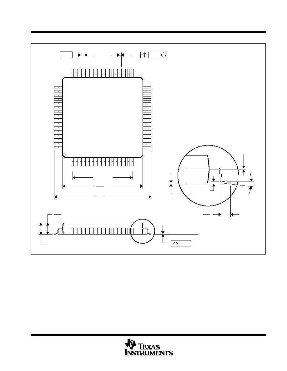
MECHANICAL DATA
MTQF008A ≠ JANUARY 1995 ≠ REVISED DECEMBER 1996
1
POST OFFICE BOX 655303
∑
DALLAS, TEXAS 75265
PM (S-PQFP-G64)
PLASTIC QUAD FLATPACK
4040152 / C 11/96
32
17
0,13 NOM
0,25
0,45
0,75
Seating Plane
0,05 MIN
Gage Plane
0,27
33
16
48
1
0,17
49
64
SQ
SQ
10,20
11,80
12,20
9,80
7,50 TYP
1,60 MAX
1,45
1,35
0,08
0,50
M
0,08
0
∞
≠ 7
∞
NOTES: A. All linear dimensions are in millimeters.
B. This drawing is subject to change without notice.
C. Falls within JEDEC MS-026
D. May also be thermally enhanced plastic with leads connected to the die pads.

IMPORTANT NOTICE
Texas Instruments Incorporated and its subsidiaries (TI) reserve the right to make corrections, modifications,
enhancements, improvements, and other changes to its products and services at any time and to discontinue
any product or service without notice. Customers should obtain the latest relevant information before placing
orders and should verify that such information is current and complete. All products are sold subject to TI's terms
and conditions of sale supplied at the time of order acknowledgment.
TI warrants performance of its hardware products to the specifications applicable at the time of sale in
accordance with TI's standard warranty. Testing and other quality control techniques are used to the extent TI
deems necessary to support this warranty. Except where mandated by government requirements, testing of all
parameters of each product is not necessarily performed.
TI assumes no liability for applications assistance or customer product design. Customers are responsible for
their products and applications using TI components. To minimize the risks associated with customer products
and applications, customers should provide adequate design and operating safeguards.
TI does not warrant or represent that any license, either express or implied, is granted under any TI patent right,
copyright, mask work right, or other TI intellectual property right relating to any combination, machine, or process
in which TI products or services are used. Information published by TI regarding third-party products or services
does not constitute a license from TI to use such products or services or a warranty or endorsement thereof.
Use of such information may require a license from a third party under the patents or other intellectual property
of the third party, or a license from TI under the patents or other intellectual property of TI.
Reproduction of information in TI data books or data sheets is permissible only if reproduction is without
alteration and is accompanied by all associated warranties, conditions, limitations, and notices. Reproduction
of this information with alteration is an unfair and deceptive business practice. TI is not responsible or liable for
such altered documentation.
Resale of TI products or services with statements different from or beyond the parameters stated by TI for that
product or service voids all express and any implied warranties for the associated TI product or service and
is an unfair and deceptive business practice. TI is not responsible or liable for any such statements.
Following are URLs where you can obtain information on other Texas Instruments products and application
solutions:
Products
Applications
Amplifiers
amplifier.ti.com
Audio
www.ti.com/audio
Data Converters
dataconverter.ti.com
Automotive
www.ti.com/automotive
DSP
dsp.ti.com
Broadband
www.ti.com/broadband
Interface
interface.ti.com
Digital Control
www.ti.com/digitalcontrol
Logic
logic.ti.com
Military
www.ti.com/military
Power Mgmt
power.ti.com
Optical Networking
www.ti.com/opticalnetwork
Microcontrollers
microcontroller.ti.com
Security
www.ti.com/security
Telephony
www.ti.com/telephony
Video & Imaging
www.ti.com/video
Wireless
www.ti.com/wireless
Mailing Address:
Texas Instruments
Post Office Box 655303 Dallas, Texas 75265
Copyright
2004, Texas Instruments Incorporated