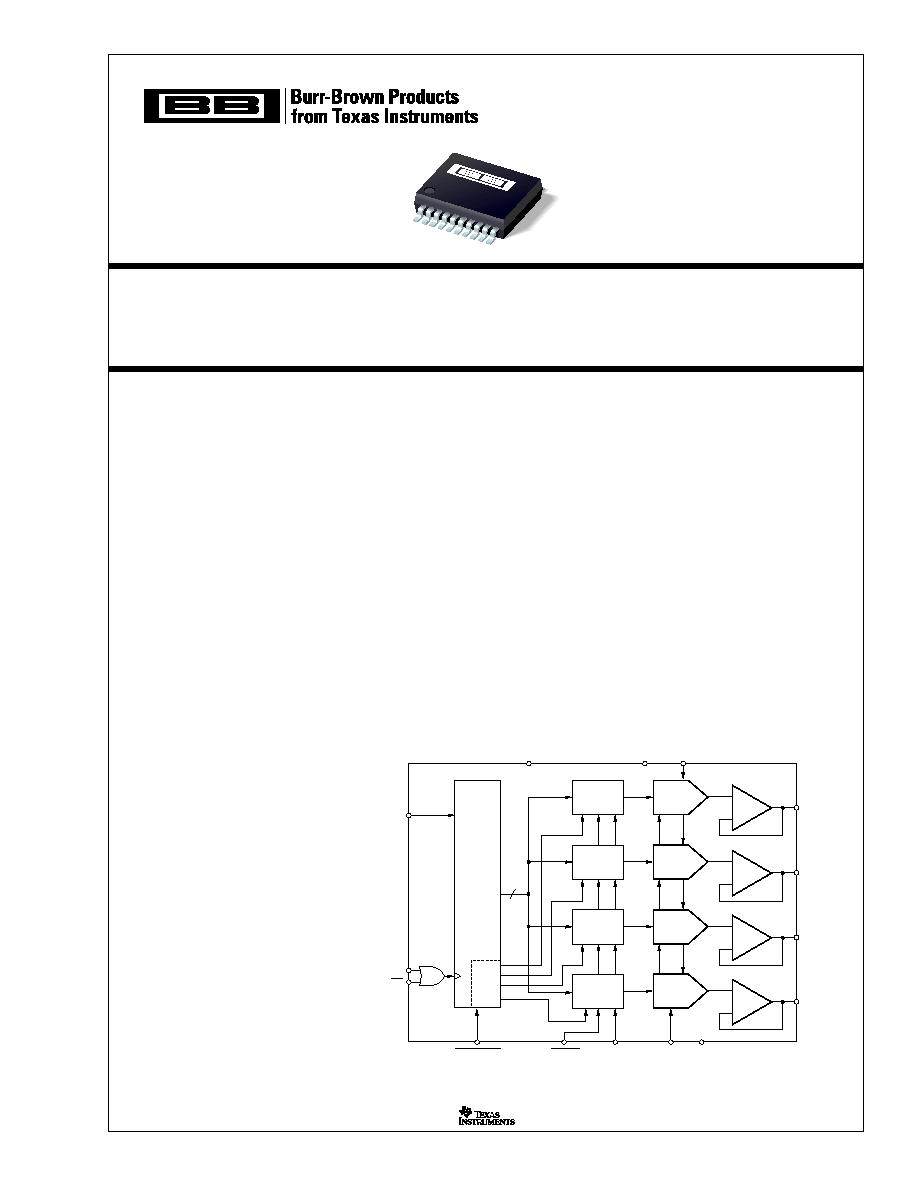
DAC7714
Copyright © 2000, Texas Instruments Incorporated
PDS-1533A
Printed in U.S.A. September, 2000
Quad, Serial Input, 12-Bit, Voltage Output
DIGITAL-TO-ANALOG CONVERTER
FEATURES
q
LOW POWER: 250mW (max)
q
UNIPOLAR OR BIPOLAR OPERATION
q
SETTLING TIME: 10
µ
s to 0.012%
q
12-BIT LINEARITY AND MONOTONICITY:
≠40
∞
C to +85
∞
C
q
USER SELECTABLE RESET TO MID-
SCALE OR ZERO-SCALE
q
SECOND-SOURCE for DAC8420
q
SMALL SO-16 PACKAGE
APPLICATIONS
q
ATE PIN ELECTRONICS
q
PROCESS CONTROL
q
CLOSED-LOOP SERVO-CONTROL
q
MOTOR CONTROL
q
DATA ACQUISITION SYSTEMS
DESCRIPTION
The DAC7714 is a quad, serial input, 12-bit, voltage
output Digital-to-Analog Converter (DAC) with guar-
anteed 12-bit monotonic performance over the ≠40
∞
C
to +85
∞
C temperature range. An asynchronous reset
clears all registers to either mid-scale (800
H
) or zero-
scale (000
H
), selectable via the RESETSEL pin. The
device can be powered from a single +15V supply or
from dual +15V and ≠15V supplies.
Low power and small size makes the DAC7714 ideal
for process control, data acquisition systems, and
closed-loop servo-control. The device is available in a
SO-16 package, and is guaranteed over the ≠40
∞
C to
+85
∞
C temperature range.
DAC A
DAC
Register A
DAC B
DAC
Register B
DAC C
DAC
Register C
DAC D
DAC
Register D
V
REFH
V
CC
V
SS
V
OUTD
V
OUTC
V
OUTB
V
OUTA
V
REFL
GND
CLK
CS
12
SDI
RESET
RESETSEL
LOADDACS
Serial-to-
Parallel
Shift
Register
DAC
Select
Æ
DAC7714
International Airport Industrial Park ∑ Mailing Address: PO Box 11400, Tucson, AZ 85734 ∑ Street Address: 6730 S. Tucson Blvd., Tucson, AZ 85706 ∑ Tel: (520) 746-1111
Twx: 910-952-1111 ∑ Cable: BBRCORP ∑ Telex: 066-6491 ∑ FAX: (520) 889-1510 ∑ Immediate Product Info: (800) 548-6132
http://www.burr-brown.com/ http://www.ti.com/
SBAS119
Æ
2
DAC7714
SPECIFICATIONS (Dual Supply)
At T
A
= ≠40
∞
C to +85
∞
C, V
CC
= +15V, V
SS
= ≠15V, V
REFH
= +10V, V
REFL
= ≠10V, unless otherwise noted.
The information provided herein is believed to be reliable; however, BURR-BROWN assumes no responsibility for inaccuracies or omissions. BURR-BROWN assumes
no responsibility for the use of this information, and all use of such information shall be entirely at the user's own risk. Prices and specifications are subject to change
without notice. No patent rights or licenses to any of the circuits described herein are implied or granted to any third party. BURR-BROWN does not authorize or warrant
any BURR-BROWN product for use in life support devices and/or systems.
DAC7714U
DAC7714UB
PARAMETER
CONDITIONS
MIN
TYP
MAX
MIN
TYP
MAX
UNITS
ACCURACY
Linearity Error
±
2
±
1
LSB
(1)
Linearity Matching
(2)
±
2
±
1
LSB
Differential Linearity Error
±
1
±
1
LSB
Monotonicity
T
MIN
to T
MAX
12
T
Bits
Zero-Scale Error
Code = 000
H
±
2
T
LSB
Zero-Scale Drift
1
T
ppm/
∞
C
Zero-Scale Matching
(2)
±
2
±
1
LSB
Full-Scale Error
Code = FFF
H
±
2
T
LSB
Full-Scale Matching
(2)
±
2
±
1
LSB
Power Supply Sensitivity
At Full Scale
10
T
ppm / V
ANALOG OUTPUT
Voltage Output
(3)
V
REFL
V
REFH
T
T
V
Output Current
≠5
+5
T
T
mA
Load Capacitance
No Oscillation
500
T
pF
Short-Circuit Current
±
20
T
mA
Short-Circuit Duration
To V
SS
, V
CC
, or GND
Indefinite
T
REFERENCE INPUT
V
REFH
Input Range
V
REFL
+1.25
+10
T
T
V
V
REFL
Input Range
≠10
V
REFH
≠ 1.25
T
T
V
Ref High Input Current
≠0.5
3.0
T
T
mA
Ref Low Input Current
≠3.5
0
T
T
mA
DYNAMIC PERFORMANCE
Settling Time
To
±
0.012%, 20V Output Step
8
10
T
T
µ
s
Channel-to-Channel Crosstalk
Full-Scale Step
0.25
T
LSB
Digital Feedthrough
2
T
nV-s
Output Noise Voltage
f = 10kHz
65
T
nV/
Hz
DIGITAL INPUT
Logic Levels
V
IH
I
IH
±
10
µ
A
3.325
T
V
V
IL
I
IL
±
10
µ
A
1.575
T
V
Data Format
Straight Binary
T
POWER SUPPLY REQUIREMENTS
V
CC
+14.25
+15.75
T
T
V
V
SS
≠15.75
≠14.25
T
T
V
I
CC
6
8.5
T
T
mA
I
SS
≠8
≠6
T
T
mA
Power Dissipation
180
250
T
T
mW
TEMPERATURE RANGE
Specified Performance
≠40
+85
T
T
∞
C
NOTES: (1) LSB means Least Significant Bit; if V
REFH
equals +10V and V
REFL
equals ≠10V, then one LSB equals 4.88mV. (2) All DAC outputs will match within
the specified error band. (3) Ideal output voltage does not take into account zero or full-scale error.
3
Æ
DAC7714
SPECIFICATIONS (Single Supply)
At T
A
= ≠40
∞
C to +85
∞
C, V
CC
= +15V, V
SS
= GND, V
REFH
= +10V, V
REFL
= 0V, unless otherwise noted.
DAC7714U
DAC7714UB
PARAMETER
CONDITIONS
MIN
TYP
MAX
MIN
TYP
MAX
UNITS
ACCURACY
Linearity Error
(1)
±
2
±
1
LSB
(2)
Linearity Matching
(3)
±
2
±
1
LSB
Differential Linearity Error
±
1
±
1
LSB
Monotonicity
T
MIN
to T
MAX
12
T
Bits
Zero-Scale Error
Code = 004
H
±
4
T
LSB
Zero-Scale Drift
2
T
ppm/
∞
C
Zero-Scale Matching
(3)
±
4
±
2
LSB
Full-Scale Error
Code = FFF
H
±
4
T
LSB
Full-Scale Matching
(3)
±
4
±
2
LSB
Power Supply Sensitivity
At Full Scale
20
T
ppm /V
ANALOG OUTPUT
Voltage Output
(4)
V
REFL
V
REFH
T
T
V
Output Current
≠5
+5
T
mA
Load Capacitance
No Oscillation
500
T
pF
Short-Circuit Current
±
20
T
mA
Short-Circuit Duration
To V
CC
or GND
Indefinite
T
REFERENCE INPUT
V
REFH
Input Range
V
REFL
+1.25
+10
T
T
V
V
REFL
Input Range
0
V
REFH
≠ 1.25
T
T
V
Ref High Input Current
≠0.3
1.5
T
T
mA
Ref Low Input Current
≠2.0
0
T
T
mA
DYNAMIC PERFORMANCE
Settling Time
(5)
To
±
0.012%, 10V Output Step
8
10
T
T
µ
s
Channel-to-Channel Crosstalk
0.25
T
LSB
Digital Feedthrough
2
T
nV-s
Output Noise Voltage
f = 10kHz
65
T
nV/
Hz
DIGITAL INPUT/OUTPUT
Logic Levels
V
IH
I
IH
±
10
µ
A
3.325
T
V
V
IL
I
IL
±
10
µ
A
1.575
T
V
Data Format
Straight Binary
T
POWER SUPPLY REQUIREMENTS
V
CC
14.25
15.75
T
T
V
I
CC
3.0
T
T
mA
Power Dissipation
45
T
mW
TEMPERATURE RANGE
Specified Performance
≠40
+85
T
T
∞
C
NOTES: (1) If V
SS
= 0V, specification applies at code 004
H
and above. (2) LSB means Least Significant Bit; if V
REFH
equals +10V and V
REFL
equals 0V, then one
LSB equals 2.44mV. (3) All DAC outputs will match within the specified error band. (4) Ideal output voltage does not take into account zero or full-scale error.
(5) Full-scale positive 10V step and negative step from code FFF
H
to 020
H
.
Æ
4
DAC7714
ELECTROSTATIC
DISCHARGE SENSITIVITY
This integrated circuit can be damaged by ESD. Burr-Brown
recommends that all integrated circuits be handled with
appropriate precautions. Failure to observe proper handling
and installation procedures can cause damage.
ESD damage can range from subtle performance degradation
to complete device failure. Precision integrated circuits may
be more susceptible to damage because very small parametric
changes could cause the device not to meet its published
specifications.
PACKAGE/ORDERING INFORMATION
MAXIMUM
MAXIMUM
LINEARITY
DIFFERENTIAL
PACKAGE
SPECIFICATION
ERROR
LINEARITY
DRAWING
TEMPERATURE
ORDERING
TRANSPORT
PRODUCT
(LSB)
(LSB)
PACKAGE
NUMBER
RANGE
NUMBER
(1)
MEDIA
DAC7714U
±
2
±
1
SO-16
211
≠40
∞
C to +85
∞
C
DAC7714U
Rails
"
"
"
"
"
"
DAC7714U/1K
Tape and Reel
DAC7714UB
±
1
±
1
SO-16
211
≠40
∞
C to +85
∞
C
DAC7714UB
Rails
"
"
"
"
"
"
DAC7714UB/1K
Tape and Reel
NOTE: (1) Models with a slash (/) are available only in Tape and Reel in the quantities indicated (e.g., /1K indicates 1000 devices per reel). Ordering 1000 pieces
of "DAC7714UB/1K" will get a single 1000-piece Tape and Reel.
REF
H
Typical of Each
Logic Input Pin
Internal V
DD
REF
L
V
SS
V
OUT
V
SS
GND
V
CC
V
CC
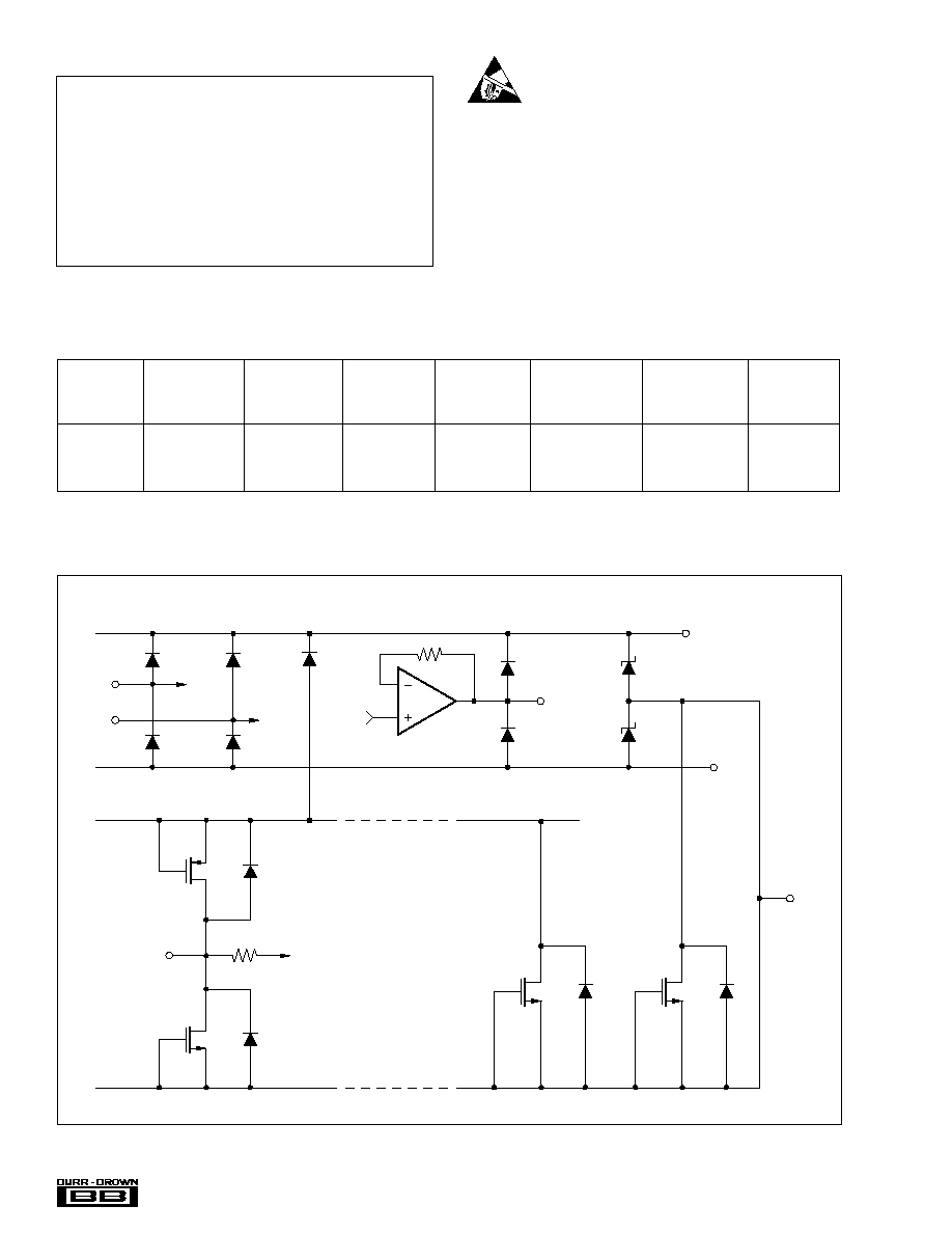
ESD PROTECTION CIRCUITS
ABSOLUTE MAXIMUM RATINGS
(1)
V
CC
to V
SS
........................................................................... ≠0.3V to +32V
V
CC
to GND ......................................................................... ≠0.3V to +16V
V
SS
to GND ......................................................................... +0.3V to ≠16V
V
REF
H to GND ....................................................................... ≠9V to +11V
V
REF
L to GND (V
SS
= ≠15V) ................................................. ≠11V to +9V
V
REF
L to GND (V
SS
= 0V) .................................................... ≠0.3V to +9V
V
REFH
to V
REFL
....................................................................... ≠1V to +22V
Digital Input Voltage to GND .............................................. ≠0.3V to 5.8V
Digital Output Voltage to GND ............................................ ≠0.3V to 5.8V
Maximum Junction Temperature ................................................... +150
∞
C
Operating Temperature Range ........................................ ≠40
∞
C to +85
∞
C
Storage Temperature Range ......................................... ≠65
∞
C to +150
∞
C
Lead Temperature (soldering, 10s) ............................................... +300
∞
C
NOTE: (1) Stresses above those listed under "Absolute Maximum Ratings"
may cause permanent damage to the device. Exposure to absolute maximum
conditions for extended periods may affect device reliability.
5
Æ
DAC7714
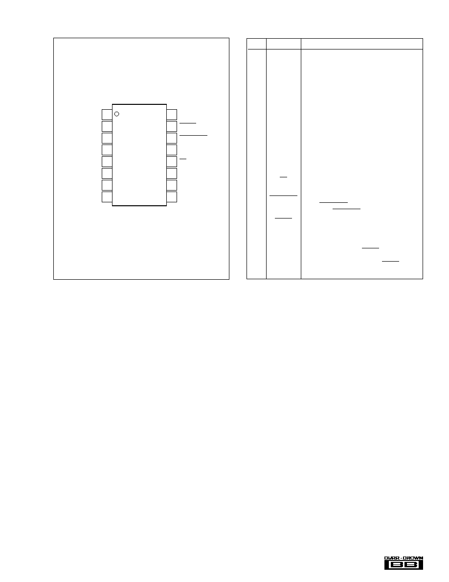
PIN CONFIGURATION--U Package
Top View
SO
PIN DESCRIPTIONS--U Package
PIN
LABEL
DESCRIPTION
1
V
CC
Positive Analog Supply Voltage, +15V nominal.
2
V
OUTD
DAC D Voltage Output
3
V
OUTC
DAC C Voltage Output
4
V
REFL
Reference Input Voltage Low. Sets minimum
output voltage for all DACs.
5
V
REFH
Reference Input Voltage High. Sets maximum
output voltage for all DACs.
6
V
OUTB
DAC B Voltage Output
7
V
OUTA
DAC A Voltage Output
8
V
SS
Negative Analog Supply Voltage, 0V or ≠15V
nominal.
9
GND
Ground
10
SDI
Serial Data Input
11
CLK
Serial Data Clock
12
CS
Chip Select Input
13
NIC
Not Internally Connected
14
LOADDACS
The selected DAC register becomes transparent
when LOADDACS is LOW. It is in the latched
state when LOADDACS is HIGH.
15
RESET
Asynchronous Reset Input. Sets all DAC
registers to either zero-scale (000
H
) or mid-
scale (800
H
) when LOW. RESETSEL determines
which code is active.
16
RESETSEL
When LOW, a LOW on RESET will cause all
DAC registers to be set to code 000
H
. When
RESETSEL is HIGH, a LOW on RESET will set
the registers to code 800
H
.
1
2
3
4
5
6
7
8
16
15
14
13
12
11
10
9
V
CC
V
OUTD
V
OUTC
V
REFL
V
REFH
V
OUTB
V
OUTA
V
SS
RESETSEL
RESET
LOADDACS
NIC
CS
CLK
SDI
GND
DAC7714U

Æ
6
DAC7714
TYPICAL PERFORMANCE CURVES: V
SS
= 0V
At T
A
= +25
∞
C, V
CC
= +15V, V
SS
= 0V, V
REFH
= +10V, V
REFL
= 0V, representative unit, unless otherwise specified.
000
H
200
H
400
H
600
H
800
H
Digital Input Code
A00
H
C00
H
E00
H
FFF
H
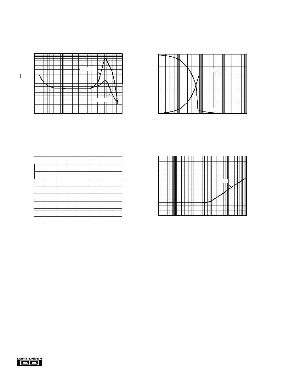
LINEARITY ERROR AND
DIFFERENTIAL LINEARITY ERROR vs CODE
Single Channel 25
∞
C
(Typical of Each Output Channel)
0.5
0.4
0.3
0.2
0.1
0
≠0.1
≠0.2
≠0.3
≠0.4
≠0.5
0.5
0.4
0.3
0.2
0.1
0
≠0.1
≠0.2
≠0.3
≠0.4
≠0.5
LE (LSB)
DLE (LSB)
0.5
0.4
0.3
0.2
0.1
0
≠0.1
≠0.2
≠0.3
≠0.4
≠0.5
0.5
0.4
0.3
0.2
0.1
0
≠0.1
≠0.2
≠0.3
≠0.4
≠0.5
LE (LSB)
DLE (LSB)
000
H
200
H
400
H
600
H
800
H
Digital Input Code
A00
H
C00
H
E00
H
FFF
H
LINEARITY ERROR AND
DIFFERENTIAL LINEARITY ERROR vs CODE
Single Channel 85
∞
C
(Typical of Each Output Channel)
000
H
200
H
400
H
600
H
800
H
Digital Input Code
A00
H
C00
H
E00
H
FFF
H
LINEARITY ERROR AND
DIFFERENTIAL LINEARITY ERROR vs CODE
Single Channel ≠40
∞
C
(Typical of Each Output Channel)
0.5
0.4
0.3
0.2
0.1
0
≠0.1
≠0.2
≠0.3
≠0.4
≠0.5
0.5
0.4
0.3
0.2
0.1
0
≠0.1
≠0.2
≠0.3
≠0.4
≠0.5
LE (LSB)
DLE (LSB)
≠30 ≠20 ≠10 0
10 20
30
40 50
60 70
80
90
≠40
Temperature (
∞
C)
ZERO-SCALE ERROR vs TEMPERATURE
(Code 004
H
)
Zero-Scale Error (mV)
2.0
1.5
1.0
0.5
0
≠0.5
≠1.0
≠1.5
≠2.0
DAC A
DAC B
DAC D
DAC C
≠30 ≠20 ≠10 0
10 20
30
40 50
60 70
80
90
≠40
Temperature (
∞
C)
FULL-SCALE ERROR vs TEMPERATURE
(Code FFF
H
)
Full-Scale Error (mV)
2.0
1.5
1.0
0.5
0
≠0.5
≠1.0
≠1.5
≠2.0
DAC C
DAC B
DAC D
DAC A
1.2
1.0
0.8
0.6
0.4
0.2
0
≠0.2
≠0.4
0
≠0.2
≠0.4
≠0.6
≠0.8
≠1.0
≠1.2
≠1.4
≠1.6
V
REF
Current (mA)
V
REF
Current (mA)
000
H
200
H
400
H
600
H
800
H
Digital Input Code
A00
H
C00
H
E00
H
FFF
H
CURRENT vs CODE
All DACs Set to Indicated Code
V
REFH
V
REFL

7
Æ
DAC7714
TYPICAL PERFORMANCE CURVES: V
SS
= 0V
(Cont.)
At T
A
= +25
∞
C, V
CC
= +15V, V
SS
= 0V, V
REFH
= +10V, V
REFL
= 0V, representative unit, unless otherwise specified.
4.5
3.5
2.5
1.5
0.5
≠0.5
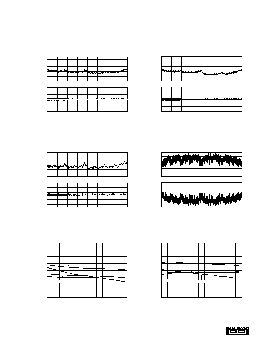
POWER SUPPLY CURRENT vs TEMPERATURE
Quiescent Current (mA)
Temperature (
∞
C)
≠40 ≠30 ≠20 ≠10 0
10 20 30 40 50 60 70 80 90 100
I
CC
I
CC
POSITIVE SUPPLY CURRENT
vs DIGITAL INPUT CODE
6.00
5.00
4.00
3.00
2.00
1.00
0
I
CC
(mA)
No Load, All 4 DACs Set to Indicated Code
200
H
400
H
600
H
800
H
A00
H
C00
H
E00
H
FFF
H
000
H
Digital Input Code
OUTPUT VOLTAGE
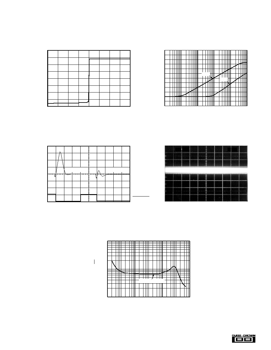
MID-SCALE GLITCH PERFORMANCE
Time (1
µ
s/div)
7FF
H
to 800
H
+5V
LOADDACS
0
Output V
oltage (200mV/div)
OUTPUT VOLTAGE
MID-SCALE GLITCH PERFORMANCE
Time (1
µ
s/div)
800
H
to 7FF
H
+5V
LOADDACS
0
Output V
oltage (200mV/div)
OUTPUT VOLTAGE vs SETTLING TIME
(0V to +10V)
Output V
oltage
Time (2
µ
s/div)
Large Signal
Settling Time: 5V/div
Small Signal
Settling Time: 1LSB/div
+5V
LOADDACS
0
OUTPUT VOLTAGE vs SETTLING TIME
(+10V to Code 020
H
)
Output V
oltage
Time (2
µ
s/div)
Large Signal
Settling Time: 5V/div
Small Signal
Settling Time: 1LSB/div
+5V
LOADDACS
0
Æ
8
DAC7714
TYPICAL PERFORMANCE CURVES: V
SS
= 0V
(Cont.)
At T
A
= +25
∞
C, V
CC
= +15V, V
SS
= 0V, V
REFH
= +10V, V
REFL
= 0V, representative unit, unless otherwise specified.
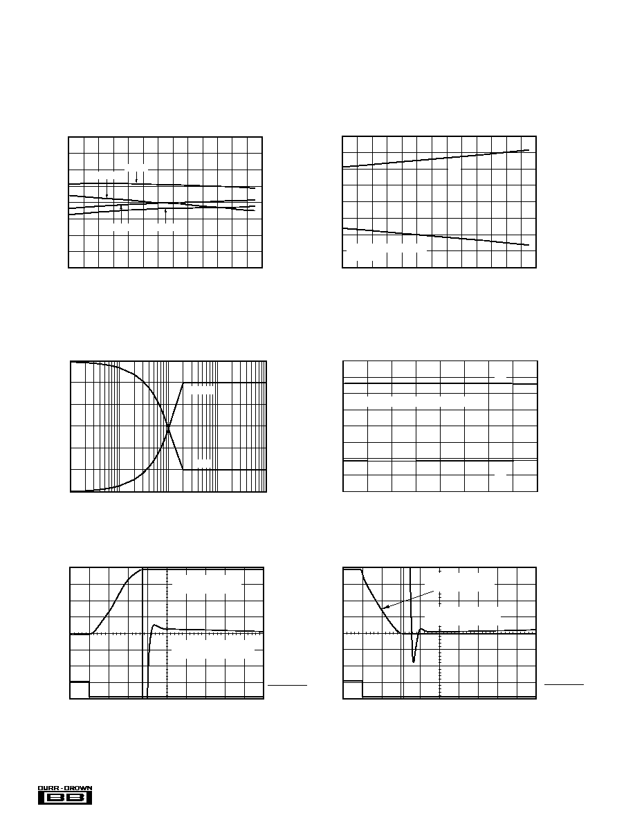
SINGLE SUPPLY CURRENT LIMIT vs INPUT CODE
20
15
10
5
0
≠5
≠10
≠15
≠20
I
OUT
(mA)
200
H
400
H
600
H
800
H
A00
H
C00
H
E00
H
FFF
H
000
H
Digital Input Code
Short to Ground
Short to V
CC
+15V
POWER SUPPLY REJECTION RATIO vs FREQUENCY
Frequency (Hz)
PSRR (dB)
0
≠10
≠20
≠30
≠40
≠50
≠60
≠70
≠80
≠90
≠100
≠110
≠120
10
2
10
3
10
4
10
5
10
6
10
1
15
12
9
6
3
0
R
LOAD
(kW)
0.01
0.1
1
10
100
OUTPUT VOLTAGE vs R
LOAD
V
OUT
(V)
Source
Sink
OUTPUT NOISE vs FREQUENCY
Frequency (kHz)
Noise (nV/
Hz)
1000
100
10
0.1
1
10
100
1000
10000
0
Code 020
H
Code FFF
H
9
Æ
DAC7714
TYPICAL PERFORMANCE CURVES: V
SS
= ≠15V
At T
A
= +25
∞
C, V
CC
= +15V, V
SS
= ≠15V, V
REFH
= +10V, V
REFL
= ≠10V, representative unit, unless otherwise specified.
000
H
200
H
400
H
600
H
800
H
Digital Input Code
A00
H
C00
H
E00
H
FFF
H
LINEARITY ERROR AND
DIFFERENTIAL LINEARITY ERROR vs CODE
Single Channel 25
∞
C
(Typical of Each Output Channel)
0.5
0.4
0.3
0.2
0.1
0
≠0.1
≠0.2
≠0.3
≠0.4
≠0.5
0.5
0.4
0.3
0.2
0.1
0
≠0.1
≠0.2
≠0.3
≠0.4
≠0.5
LE (LSB)
DLE (LSB)
000
H
200
H
400
H
600
H
800
H
Digital Input Code
A00
H
C00
H
E00
H
FFF
H
LINEARITY ERROR AND
DIFFERENTIAL LINEARITY ERROR vs CODE
Single Channel 85
∞
C
(Typical of Each Output Channel)
0.5
0.4
0.3
0.2
0.1
0
≠0.1
≠0.2
≠0.3
≠0.4
≠0.5
0.5
0.4
0.3
0.2
0.1
0
≠0.1
≠0.2
≠0.3
≠0.4
≠0.5
LE (LSB)
DLE (LSB)
000
H
200
H
400
H
600
H
800
H
Digital Input Code
A00
H
C00
H
E00
H
FFF
H
LINEARITY ERROR AND
DIFFERENTIAL LINEARITY ERROR vs CODE
Single Channel ≠40
∞
C
(Typical of Each Output Channel)
0.5
0.4
0.3
0.2
0.1
0
≠0.1
≠0.2
≠0.3
≠0.4
≠0.5
0.5
0.4
0.3
0.2
0.1
0
≠0.1
≠0.2
≠0.3
≠0.4
≠0.5
LE (LSB)
DLE (LSB)
2.5
2.0
1.5
1.0
0.5
0
≠0.5
V
REF
Current (mA)
CURRENT vs CODE
All DACs Set to Indicated Code
V
REFH
V
REFL
000
H
200
H
400
H
600
H
800
H
Digital Input Code
A00
H
C00
H
E000
H
FFF
H
0
≠0.5
≠1.0
≠1.5
≠2.0
≠2.5
≠3.0
V
REF
Current (mA)
≠30 ≠20 ≠10 0
10 20
30
40 50
60 70
80
90
≠40
Temperature (
∞
C)
BIPOLAR ZERO-SCALE ERROR vs TEMPERATURE
(Code 800
H
)
Bipolar Zero-Scale Error (mV)
DAC C
DAC A
DAC D
DAC B
2.0
1.5
1.0
0.5
0
≠0.5
≠1.0
≠1.5
≠2.0
≠30 ≠20 ≠10 0
10 20
30
40 50
60 70
80
90
≠40
Temperature (
∞
C)
POSITIVE FULL-SCALE ERROR vs TEMPERATURE
(Code FFF
H
)
Positive Full-Scale Error (mV)
2.0
1.5
1.0
0.5
0
≠0.5
≠1.0
≠1.5
≠2.0
DAC D
DAC C
DAC A
DAC B
Æ
10
DAC7714
TYPICAL PERFORMANCE CURVES: V
SS
= ≠15V
(Cont.)
At T
A
= +25
∞
C, V
CC
= +15V, V
SS
= ≠15V, V
REFH
= +10V, V
REFL
= ≠10V, representative unit, unless otherwise specified.
≠30 ≠20 ≠10 0
10 20
30
40 50
60 70
80
90
≠40
Temperature (
∞
C)
NEGATIVE FULL-SCALE ERROR vs TEMPERATURE
(Code 000
H
)
Negative Full-Scale Error (mV)
DAC A
DAC C
DAC D
DAC B
2.0
1.5
1.0
0.5
0
≠0.5
≠1.0
≠1.5
≠2.0
8
6
4
2
0
≠2
≠4
≠6
≠8
Data = FFF
H
(all DACs)
No Load
POWER SUPPLY CURRENT vs TEMPERATURE
Quiescent Current (mA)
Temperature (
∞
C)
≠40 ≠30 ≠20 ≠10
0
10 20
30
40 50
60
70 80 90
I
CC
I
SS
15
10
5
0
≠5
≠10
≠15
R
LOAD
(k
)
0.01
0.1
1
10
100
OUTPUT VOLTAGE vs R
LOAD
V
OUT
(V)
Sink
Source
SUPPLY CURRENT vs CODE
8
6
4
2
0
≠2
≠4
≠6
≠8
Supply Current (mA)
I
SS
200
H
400
H
600
H
800
H
A00
H
C00
H
E00
H
FFF
H
000
H
Digital Input Code
I
CC
No Load, All 4 DACs Set to Indicated Code
OUTPUT VOLTAGE vs SETTLING TIME
(≠10V to +10V)
Output V
oltage
Time (2
µ
s/div)
Large Signal
Settling Time: 5V/div
Small Signal
Settling Time: 0.5LSB/div
+5V
LOADDACS
0
OUTPUT VOLTAGE vs SETTLING TIME
(+10V to ≠10V)
Output V
oltage
Time (2
µ
s/div)
Small Signal
Settling Time: 0.5LSB/div
Large Signal
Settling Time: 5V/div
+5V
LOADDACS
0
11
Æ
DAC7714
BROADBAND NOISE
Time (1ms/div)
Noise Voltage (500
µ
V/div)
TYPICAL PERFORMANCE CURVES: V
SS
= ≠15V
(Cont.)
At T
A
= +25
∞
C, V
CC
= +15V, V
SS
= ≠15V, V
REFH
= +10V, V
REFL
= ≠10V, representative unit, unless otherwise specified.
DUAL SUPPLY CURRENT LIMIT vs INPUT CODE
SHORT TO GROUND
20
15
10
5
0
≠5
≠10
≠15
≠20
I
OUT
(mA)
200
H
400
H
600
H
800
H
A00
H
C00
H
E00
H
FFF
H
000
H
Digital Input Code
≠15V
POWER SUPPLY REJECTION RATIO vs FREQUENCY
Frequency (Hz)
PSRR (dB)
0
≠10
≠20
≠30
≠40
≠50
≠60
≠70
≠80
≠90
≠100
≠110
≠120
10
2
10
3
10
4
10
5
10
6
10
1
+15V
OUTPUT VOLTAGE
MID-SCALE GLITCH PERFORMANCE
Time (1
µ
s/div)
+5V
LOADDACS
0
Output V
oltage (200mV/div)
7FF
H
to 800
H
800
H
to 7FF
H
Noise at any code
OUTPUT NOISE vs FREQUENCY
Frequency (kHz)
Noise (nV/
Hz)
1000
100
10
0.1
1
10
100
1000
10000
0
Æ
12
DAC7714
THEORY OF OPERATION
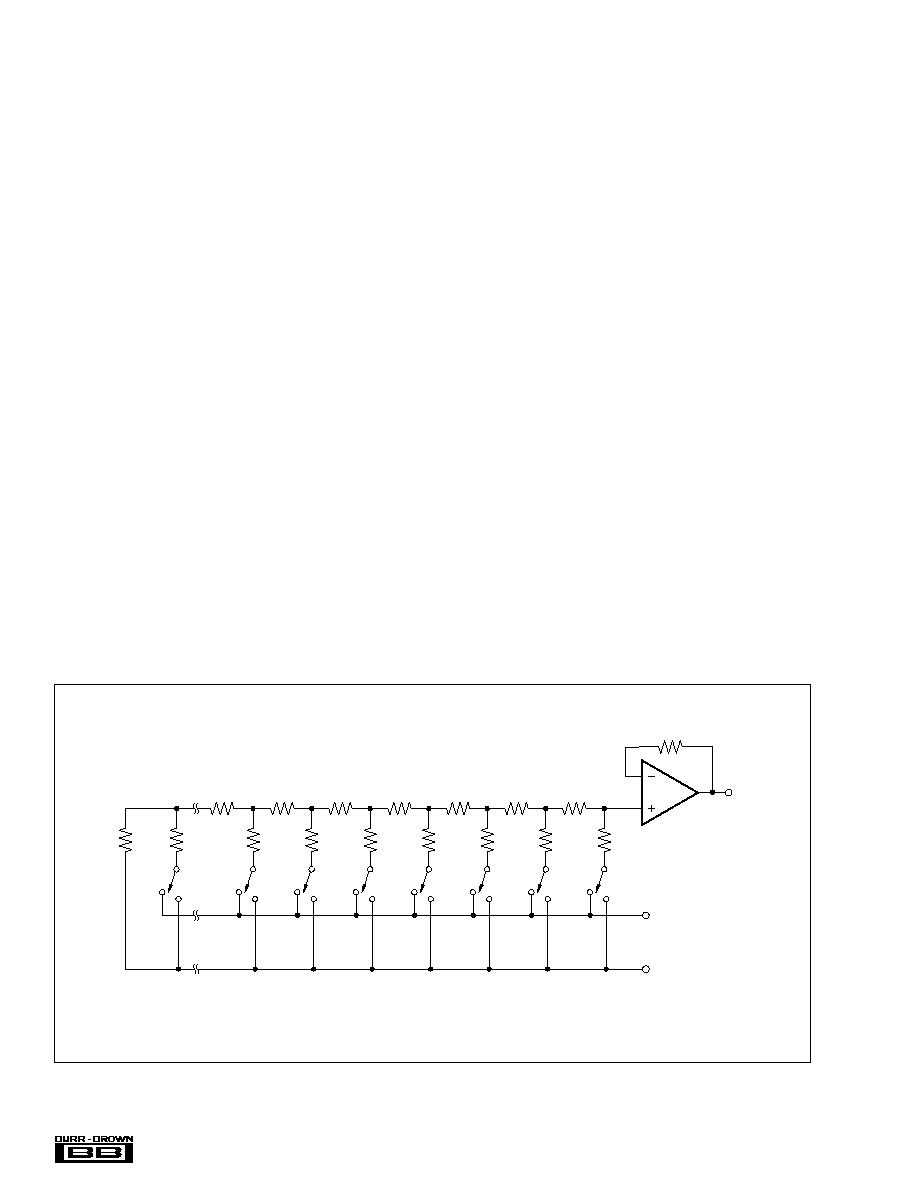
The DAC7714 is a quad, serial input, 12-bit, voltage output
DAC. The architecture is a classic R-2R ladder configura-
tion followed by an operational amplifier that serves as a
buffer. Each DAC has its own R-2R ladder network and
output op amp, but all share the reference voltage inputs, as
shown in Figure 1. The minimum voltage output ("zero-
scale") and maximum voltage output ("full-scale") are set by
external voltage references (V
REFL
and V
REFH
, respectively).
The digital input is a 16-bit serial word that contains the
12-bit DAC code and a 2-bit address code that selects one of
the four DACs (the two remaining bits are unused). The
converter can be powered from a single +15V supply or a
dual
±
15V supply. Each device offers a reset function which
immediately sets all DAC output voltages and internal
registers to either zero-scale (code 000
H
) or mid-scale (code
800
H
). The reset code is selected by the state of the
RESETSEL pin (LOW = 000
H
, HIGH = 800
H
). Figures 2
and 3 show the basic operation of the DAC7714.
ANALOG OUTPUTS
When V
SS
= ≠15V (dual supply operation), the output
amplifier can swing to within 4V of the supply rails, over the
≠40
∞
C to +85
∞
C temperature range. With V
SS
= 0V (single-
supply operation), the output can swing to ground. Note that
the settling time of the output op amp will be longer with
voltages very near ground. Care must also be taken when
measuring the zero-scale error when V
SS
= 0V. If the output
amplifier has a negative offset, the output voltage may not
change for the first few digital input codes (000
H
, 001
H
,
002
H
, etc.) since the output voltage cannot swing below
ground.
FIGURE 1. DAC7714 Architecture.
R
2R
2R
2R
2R
2R
2R
2R
2R
2R
V
REF
H
V
OUT
R
R
R
R
R
R
V
REF
L
R
F
At the negative offset limit of ≠4LSB (≠9.76mV), for the
single-supply case, the first specified output starts at code
004
H
.
REFERENCE INPUTS
The reference inputs, V
REFL
and V
REFH
, can be any voltage
between V
SS
+ 4V and V
CC
≠ 4V provided that V
REFH
is at
least 1.25V greater than V
REFL
. The minimum output of
each D/A is equal to V
REFL
≠ 1LSB plus a small offset
voltage (essentially, the offset of the output op amp). The
maximum output is equal to V
REFH
plus a similar offset
voltage. Note that V
SS
(the negative power supply) must
either be connected to ground or must be in the range of
≠14.75V to ≠15.75V. The voltage on V
SS
sets several bias
points within the converter. If V
SS
is not in one of these two
configurations, the bias values may be in error and proper
operation of the device is not guaranteed.
The current into the reference inputs depends on the DAC
output voltages and can vary from a few microamps to
approximately 3mA. The reference input appears as a vary-
ing load to the reference. If the reference can sink or source
the required current, a reference buffer is not required. See
"Reference Current vs Code" in the Typical Performance
Curves.
The analog supplies must come up before the reference
power supplies, if they are separate. If the power supplies for
the references come up first, then the V
CC
and V
SS
supplies
will be powered from the reference via the ESD protection
diodes (see page 4).

13
Æ
DAC7714
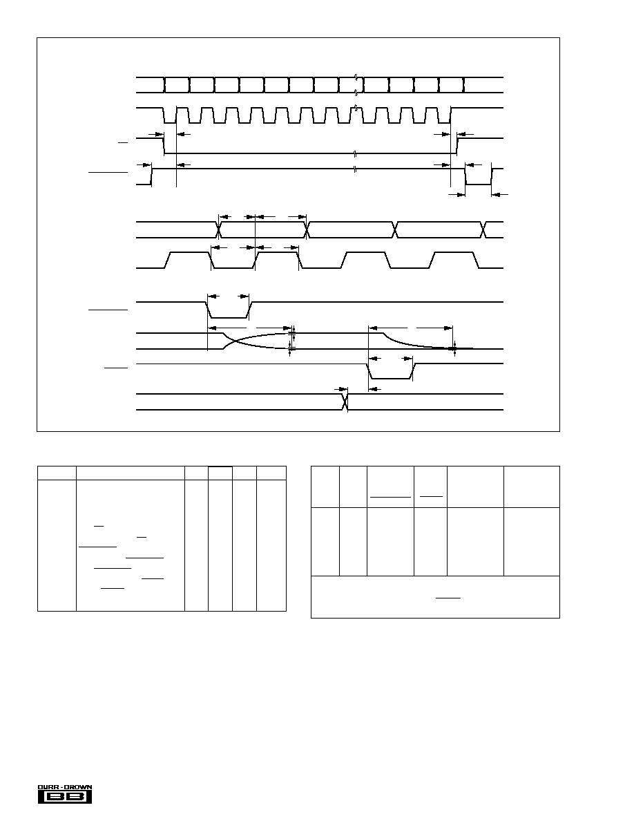
Note that CS and CLK are combined with an OR gate and
the output controls the serial-to-parallel shift register inter-
nal to the DAC7714 (see the block diagram on the front of
this data sheet). These two inputs are completely inter-
changeable. In addition, care must be taken with the state of
CLK when CS rises at the end of a serial transfer. If CLK is
LOW when CS rises, the OR gate will provide a rising edge
to the shift register, shifting the internal data one additional
bit. The result will be incorrect data and possible selection of
the wrong DAC.
If both CS and CLK are used, then CS should rise only when
CLK is HIGH. If not, then either CS or CLK can be used to
operate the shift register. See Table III for more information.
DIGITAL INTERFACE
Figure 4 and Table I provide the basic timing for the
DAC7714. The interface consists of a serial clock (CLK),
serial data (SDI), and a load DAC signal (LOADDACS). In
addition, a chip select (CS) input is available to enable serial
communication when there are multiple serial devices. An
asynchronous reset input (RESET) is provided to simplify
start-up conditions, periodic resets, or emergency resets to a
known state.
The DAC code and address are provided via a 16-bit serial
interface (see Figure 4). The first two bits select the DAC
register that will be updated when LOADDACS goes LOW
(see Table II). The next two bits are not used. The last 12 bits
is the DAC code which is provided, most significant bit first.
FIGURE 3. Basic Dual-Supply Operation of the DAC7714.
NOTE: (1) As configured, RESET LOW sets all internal registers to code 800
H
(0V).
If RESETSEL is LOW, RESET LOW sets all internal registers to code 000
H
(≠10V).
1
2
3
4
5
6
7
8
16
15
14
13
12
11
10
9
V
CC
V
OUTD
V
OUTC
V
REFL
V
REFH
V
OUTB
V
OUTA
V
SS
RESETSEL
RESET
LOADDACS
NIC
CS
CLK
SDI
GND
Reset DACs
(1)
Update Selected Register
Chip Select
Clock
Serial Data In
DAC7714
0.1
µ
F
0.1
µ
F
≠10V to +10V
1
µ
F to 10
µ
F
+15V
≠15V
+
0.1
µ
F
1
µ
F to 10
µ
F
+
≠10V to +10V
≠10.0V
0.1
µ
F
+10.0V
≠10V to +10V
≠10V to +10V
+5V
FIGURE 2. Basic Single-Supply Operation of the DAC7714.
NOTE: (1) As configured, RESET LOW sets all internal registers to code 000
H
(0V).
If RESETSEL is HIGH, RESET LOW sets all internal registers to code 800
H
(5V).
1
2
3
4
5
6
7
8
16
15
14
13
12
11
10
9
V
CC
V
OUTD
V
OUTC
V
REFL
V
REFH
V
OUTB
V
OUTA
V
SS
RESETSEL
RESET
LOADDACS
NIC
CS
CLK
SDI
GND
Reset DACs
(1)
Update Selected Register
Chip Select
Clock
Serial Data In
DAC7714
0.1
µ
F
0.1
µ
F
0V to +10.0V
1
µ
F to 10
µ
F
+15V
+
0V to +10.0V
0V to +10.0V
0V to +10.0V
+10.000V
Æ
14
DAC7714
SYMBOL
DESCRIPTION
MIN
TYP
MAX
UNITS
t
DS
Data Valid to CLK Rising
25
ns
t
DH
Data Held Valid after CLK Rises
20
ns
t
CH
CLK HIGH
30
ns
t
CL
CLK LOW
50
ns
t
CSS
CS LOW to CLK Rising
55
ns
t
CSH
CLK HIGH to CS Rising
15
ns
t
LD1
LOADDACS HIGH to CLK Rising
40
ns
t
LD2
CLK Rising to LOADDACS LOW
15
ns
t
LDDW
LOADDACS LOW Time
45
ns
t
RSSH
RESETSEL Valid to RESET LOW
25
ns
t
RSTW
RESET LOW Time
70
ns
t
S
Settling Time
10
µ
s
FIGURE 4. DAC7714 Timing.
TABLE I. Timing Specifications (T
A
= ≠40
∞
C to +85
∞
C).
A1
(MSB)
(LSB)
SDI
CLK
CS
LOADDACS
A0
X
X
D11
D10
D9
D3
D2
D1
D0
SDI
CLK
LOADDACS
RESET
V
OUT
tcss
t
LD1
t
CL
t
CH
t
DS
t
DH
t
LD2
t
LDDW
t
LDDW
t
S
t
RSTW
t
RSSH
t
CSH
t
S
1 LSB
ERROR BAND
1 LSB
ERROR BAND
RESETSEL
STATE OF
SELECTED
SELECTED
DAC
DAC
A1
A0
LOADDACS
RESET
REGISTER
REGISTER
L
(1)
L
L
H
(2)
A
Transparent
L
H
L
H
B
Transparent
H
L
L
H
C
Transparent
H
H
L
H
D
Transparent
X
(3)
X
H
H
NONE
(All Latched)
X
X
X
L
ALL
Reset
(4)
NOTES: (1) L = Logic LOW. (2) H = Logic HIGH. (3) X = Don't Care.
(4) Resets to either 000H or 800
H
, per the RESETSEL state
(LOW = 000
H
, HIGH = 800
H
). When RESET rises, all registers that are in
their latched state retain the reset value.
TABLE II. Control Logic Truth Table.
15
Æ
DAC7714
Digital Input Coding
The DAC7714 input data is in Straight Binary format. The
output voltage is given by the following equation:
V
V
V
V
N
OUT
REFL
REFH
REFL
=
+
∑
(
≠
)
4096
where N is the digital input code (in decimal). This equation
does not include the effects of offset (zero-scale) or gain
(full-scale) errors.
LAYOUT
A precision analog component requires careful layout, ad-
equate bypassing, and clean, well-regulated power supplies.
As the DAC7714 offers single-supply operation, it will often
be used in close proximity with digital logic, microcontrollers,
microprocessors, and digital signal processors. The more
digital logic present in the design and the higher the switch-
ing speed, the more difficult it will be to achieve good
performance from the converter.
Because the DAC7714 has a single ground pin, all return
currents, including digital and analog return currents, must
flow through the GND pin. Ideally, GND would be con-
nected directly to an analog ground plane. This plane would
be separate from the ground connection for the digital
components until they were connected at the power entry
point of the system.
The power applied to V
CC
(as well as V
SS
, if not grounded)
should be well regulated and low noise. Switching power
supplies and DC/DC converters will often have high-fre-
quency glitches or spikes riding on the output voltage. In
addition, digital components can create similar high-fre-
quency spikes as their internal logic switches states. This
noise can easily couple into the DAC output voltage through
various paths between the power connections and analog
output.
CS
(1)
CLK
(1)
LOADDACS
RESET
SERIAL SHIFT REGISTER
H
(2)
X
(3)
H
H
No Change
L
(4)
L
H
H
No Change
L
(5)
H
H
Advanced One Bit
L
H
H
Advanced One Bit
H
(6)
X
L
(7)
H
No Change
H
(6)
X
H
L
(8)
No Change
NOTES: (1) CS and CLK are interchangeable. (2) H = Logic HIGH. (3) X =
Don't Care. (4) L = Logic LOW (5) = Positive Logic Transition. (6) A HIGH
value is suggested in order to avoid a "false clock" from advancing the shift
register and changing the shift register. (7) If data is clocked into the serial
register while LOADDACS is LOW, the selected DAC register will change as
the shift register bits "flow" through A1 and A0. This will corrupt the data in
each DAC register that has been erroneously selected. (8) RESET LOW
causes no change in the contents of the serial shift register.
TABLE III. Serial Shift Register Truth Table.
PACKAGING INFORMATION
ORDERABLE DEVICE
STATUS(1)
PACKAGE TYPE
PACKAGE DRAWING
PINS
PACKAGE QTY
DAC7714U
ACTIVE
SOIC
DW
16
48
DAC7714U/1K
ACTIVE
SOIC
DW
16
1000
DAC7714UB
ACTIVE
SOIC
DW
16
48
DAC7714UB/1K
ACTIVE
SOIC
DW
16
1000
(1) The marketing status values are defined as follows:
ACTIVE: Product device recommended for new designs.
LIFEBUY: TI has announced that the device will be discontinued, and a lifetime-buy period is in effect.
NRND: Not recommended for new designs. Device is in production to support existing customers, but TI does not recommend using this part in
a new design.
PREVIEW: Device has been announced but is not in production. Samples may or may not be available.
OBSOLETE: TI has discontinued the production of the device.
PACKAGE OPTION ADDENDUM
www.ti.com
3-Oct-2003

IMPORTANT NOTICE
Texas Instruments Incorporated and its subsidiaries (TI) reserve the right to make corrections, modifications,
enhancements, improvements, and other changes to its products and services at any time and to discontinue
any product or service without notice. Customers should obtain the latest relevant information before placing
orders and should verify that such information is current and complete. All products are sold subject to TI's terms
and conditions of sale supplied at the time of order acknowledgment.
TI warrants performance of its hardware products to the specifications applicable at the time of sale in
accordance with TI's standard warranty. Testing and other quality control techniques are used to the extent TI
deems necessary to support this warranty. Except where mandated by government requirements, testing of all
parameters of each product is not necessarily performed.
TI assumes no liability for applications assistance or customer product design. Customers are responsible for
their products and applications using TI components. To minimize the risks associated with customer products
and applications, customers should provide adequate design and operating safeguards.
TI does not warrant or represent that any license, either express or implied, is granted under any TI patent right,
copyright, mask work right, or other TI intellectual property right relating to any combination, machine, or process
in which TI products or services are used. Information published by TI regarding third-party products or services
does not constitute a license from TI to use such products or services or a warranty or endorsement thereof.
Use of such information may require a license from a third party under the patents or other intellectual property
of the third party, or a license from TI under the patents or other intellectual property of TI.
Reproduction of information in TI data books or data sheets is permissible only if reproduction is without
alteration and is accompanied by all associated warranties, conditions, limitations, and notices. Reproduction
of this information with alteration is an unfair and deceptive business practice. TI is not responsible or liable for
such altered documentation.
Resale of TI products or services with statements different from or beyond the parameters stated by TI for that
product or service voids all express and any implied warranties for the associated TI product or service and
is an unfair and deceptive business practice. TI is not responsible or liable for any such statements.
Following are URLs where you can obtain information on other Texas Instruments products and application
solutions:
Products
Applications
Amplifiers
amplifier.ti.com
Audio
www.ti.com/audio
Data Converters
dataconverter.ti.com
Automotive
www.ti.com/automotive
DSP
dsp.ti.com
Broadband
www.ti.com/broadband
Interface
interface.ti.com
Digital Control
www.ti.com/digitalcontrol
Logic
logic.ti.com
Military
www.ti.com/military
Power Mgmt
power.ti.com
Optical Networking
www.ti.com/opticalnetwork
Microcontrollers
microcontroller.ti.com
Security
www.ti.com/security
Telephony
www.ti.com/telephony
Video & Imaging
www.ti.com/video
Wireless
www.ti.com/wireless
Mailing Address:
Texas Instruments
Post Office Box 655303 Dallas, Texas 75265
Copyright
2003, Texas Instruments Incorporated