 | –≠–ª–µ–∫—Ç—Ä–æ–Ω–Ω—ã–π –∫–æ–º–ø–æ–Ω–µ–Ω—Ç: DAC7801LU | –°–∫–∞—á–∞—Ç—å:  PDF PDF  ZIP ZIP |

DESCRIPTION
The DAC7800, DAC7801 and DAC7802 are members of a
new family of monolithic dual 12-bit CMOS multiplying Digi-
tal-to-Analog Converters (DACs). The digital interface speed
and the AC multiplying performance are achieved by using
an advanced CMOS process optimized for data conversion
circuits. High stability on-chip resistors provide true 12-bit
integral and differential linearity over the wide industrial
temperature range of ≠40
∞
C to +85
∞
C.
DAC7800 features a serial interface capable of clocking-in
data at a rate of at least 10MHz. Serial data is clocked (edge
triggered) MSB first into a 24-bit shift register and then
latched into each DAC separately or simultaneously as
required by the application. An asynchronous CLEAR control
is provided for power-on reset or system calibration func-
tions. It is packaged in a 16-pin 0.3" wide plastic DIP.
DAC7801 has a 2-byte (8 + 4) double-buffered interface.
Data is first loaded (level transferred) into the input registers
in two steps for each DAC. Then both DACs are updated
simultaneously. DAC7801 features an asynchronous CLEAR
control. DAC7801 is packaged in a 24-pin 0.3" wide plastic
DIP.
DAC7802 has a single-buffered 12-bit data word interface.
Parallel data is loaded (edge triggered) into the single DAC
register for each DAC. DAC7802 is packaged in a 24-pin 0.3"
wide plastic DIP.
FEATURES
q
TWO DACs IN A 0.3" WIDE PACKAGE
q
SINGLE +5V SUPPLY
q
HIGH SPEED DIGITAL INTERFACE:
Serial--DAC7800
8 + 4-Bit Parallel--DAC7801
12-Bit Parallel--DAC7802
q
MONOTONIC OVER TEMPERATURE
q
LOW CROSSTALK: ≠94dB min
q
FULLY SPECIFIED OVER ≠40
O
C TO +85
O
C
APPLICATIONS
q
PROCESS CONTROL OUTPUTS
q
ATE PIN ELECTRONICS LEVEL SETTING
q
PROGRAMMABLE FILTERS
q
PROGRAMMABLE GAIN CIRCUITS
q
AUTO-CALIBRATION CIRCUITS
Dual Monolithic CMOS 12-Bit Multiplying
DIGITAL-TO-ANALOG CONVERTERS
Serial Interface
8-Bit Interface
8 Bits + 4 Bits
Serial
DAC7801
DAC7800
12-Bit MDAC
DAC A
FB B
I
OUT B
CLR
WR
A0
CS
A1
UPD
UPD A
UPD B
CS
CLK
CLR
12-Bit MDAC
DAC B
R
12-Bit Interface
DAC7802
CSA
WR
12
8
CSB
12
12
AGND B
REF B
V
FB A
I
OUT A
R
AGND A
REF A
V
DAC7800
DAC7801
DAC7802
SBAS005A ≠ DECEMBER 2001
www.ti.com
PRODUCTION DATA information is current as of publication date.
Products conform to specifications per the terms of Texas Instruments
standard warranty. Production processing does not necessarily include
testing of all parameters.
Copyright © 1990, Texas Instruments Incorporated
Please be aware that an important notice concerning availability, standard warranty, and use in critical applications of
Texas Instruments semiconductor products and disclaimers thereto appears at the end of this data sheet.

DAC7800, 7801, 7802
2
SBAS005A
www.ti.com
SPECIFIED
RELATIVE
GAIN
PACKAGE
TEMPERATURE
PACKAGE
ORDERING
TRANSPORT
PRODUCT
ACCURACY
ERROR
PACKAGE-LEAD
DESIGNATOR
(1)
RANGE
MARKING
NUMBER
MEDIA, QUANTITY
DAC7800KP
±
1LSB
±
3LSB
DIP-16
N
≠40
∞
C to +85
∞
C
DAC7800KP
DAC7800KP
Rails, 25
DAC7800LP
±
1/2 LSB
±
1LSB
DIP-16
N
DAC7800LP
DAC7800LP
Rails, 25
DAC7800KU
--
--
SO-16
DW
≠40
∞
C to +85
∞
C
DAC7800KU DAC7800KU/1K Tape and Reel, 1000
DAC7800LU
--
--
SO-16
DW
DAC7800LU
DAC7800LU/1K Tape and Reel, 1000
DAC7801KP
±
1LSB
±
3LSB
DIP-24
NT
≠40
∞
C to +85
∞
C
DAC7801KP
DAC7801KP
Rails, 15
DAC7801LP
±
1/2 LSB
±
1LSB
DIP-24
NT
DAC7801LP
DAC7801LP
Rails, 15
DAC7801KU
--
--
SO-24
DW
≠40
∞
C to +85
∞
C
DAC7801KU DAC7801KU/1K Tape and Reel, 1000
DAC7801LU
--
--
SO-24
DW
DAC7801LU
DAC7801LU/1K Tape and Reel, 1000
DAC7802KP
±
1LSB
±
3LSB
DIP-24
NTG
≠40
∞
C to +85
∞
C
DAC7802KP
DAC7802KP
Rails, 15
DAC7802LP
±
1/2 LSB
±
1LSB
DIP-24
NTG
DAC7802LP
DAC7802LP
Rails, 15
DAC7802KU
--
--
SO-24
DW
≠40
∞
C to +85
∞
C
DAC7802KU DAC7802KU/1K Tape and Reel, 1000
DAC7802LU
--
--
SO-24
DW
DAC7802LU
DAC7802LU/1K Tape and Reel, 1000
NOTE: (1 ) For the most current specifications and package information, refer to our web site at www.ti.com.
ELECTRICAL CHARACTERISTICS
At V
DD
= +5VDC, V
REF A
= V
REF B
= +10V, T
A
= ≠40
∞
C to +85
∞
C, unless otherwise noted.
DAC7800, 7801, 7802K
DAC7800, 7801, 7802L
PARAMETER
CONDITIONS
MIN
TYP
MAX
MIN
TYP
MAX
UNITS
ACCURACY
Resolution
12
Bits
Relative Accuracy
±
1
±
1/2
LSB
Differential Nonlinearity
±
1
LSB
Gain Error
Measured Using R
FB A
and R
FB B
.
±
3
±
1
LSB
All Registers Loaded with All 1s.
Gain Temperature Coefficient
(1)
2
5
ppm/
∞
C
Output Leakage Current
T
A
= +25
∞
C
0.005
10
nA
T
A
= ≠40
∞
C to +85
∞
C
3
150
nA
REFERENCE INPUT
Input Resistance
6
10
14
k
Input Resistance Match
0.5
3
2
%
DIGITAL INPUTS
V
IH
(Input HIGH Voltage)
2
V
V
IL
(Input LOW Voltage)
0.8
V
I
IN
(Input Current)
T
A
= +25
∞
C
±
1
µ
A
T
A
= ≠40
∞
C to +85
∞
C
±
10
µ
A
C
IN
(Input Capacitance)
0.8
10
pF
POWER SUPPLY
V
DD
4.5
5.5
V
I
DD
0.2
2
mA
Power-Supply Rejection
V
DD
from 4.5V to 5.5V
0.002
%/%
Same specification as for DAC7800, 7801, 7802K.
V
DD
to AGND .................................................................................. 0V, +7V
V
DD
to DGND .................................................................................. 0V, +7V
AGND to DGND .......................................................................... ≠0.3, V
DD
Digital Input to DGND ........................................................ ≠0.3, V
DD
+ 0.3
V
REF A
, V
REF B
to AGND .....................................................................
±
16V
V
REF A
, V
REF B
to DGND .....................................................................
±
16V
I
OUT A
, I
OUT B
to AGND ................................................................. ≠0.3, V
DD
Storage Temperature Range ........................................... ≠55
∞
C to +125
∞
C
Operating Temperature Range ......................................... ≠40
∞
C to +85
∞
C
Lead Temperature (soldering, 10s) ................................................. +300
∞
C
Junction Temperature ...................................................................... +175
∞
C
ABSOLUTE MAXIMUM RATINGS
At T
A
= +25
∞
C, unless otherwise noted.
ELECTROSTATIC
DISCHARGE SENSITIVITY
This integrated circuit can be damaged by ESD. Texas Instru-
ments recommends that all integrated circuits be handled with
appropriate precautions. Failure to observe proper handling
and installation procedures can cause damage.
ESD damage can range from subtle performance degradation
to complete device failure. Precision integrated circuits may be
more susceptible to damage because very small parametric
changes could cause the device not to meet its published
specifications.
PACKAGE/ORDERING INFORMATION
DAC7800, 7801, 7802
3
SBAS005A
www.ti.com
AC PERFORMANCE
OUTPUT OP AMP IS OPA602.
At V
DD
= +5VDC, V
REF A
= V
REF B
= +10V, T
A
= +25
∞
C, unless otherwise noted. These specifications are fully characterized but not subject to test.
NOTE: (1) Ensured but not tested.
DAC7800, 7801, 7802K
DAC7800, 7801, 7802L
PARAMETER
CONDITIONS
MIN
TYP
MAX
MIN
TYP
MAX
UNITS
OUTPUT CURRENT SETTLING TIME
To 0.01% of Full-Scale
0.4
0.8
µ
s
R
L
= 100
, C
L
= 13pF
DIGITAL-TO-ANALOG GLITCH IMPULSE
V
REF A
= V
REF B
= 0V
0.9
nV-s
R
L
= 100
, C
L
= 13pF
AC FEEDTHROUGH
f
VREF
= 10kHz
≠75
≠72
dB
OUTPUT CAPACITANCE
DAC Loaded with All 0s
30
50
pF
DAC Loaded with All 1s
70
100
pF
CHANNEL-TO-CHANNEL ISOLATION
V
REF A
to I
OUT B
f
VREF A
= 10kHz
≠90
≠94
dB
V
REF B
= 0V,
Both DACs Loaded with 1s
V
REF B
to I
OUT A
f
VREF B
= 10kHz
≠90
≠101
dB
V
REF A
= 0V,
Both DACs Loaded with 1s
DIGITAL CROSSTALK
Full-Scale Transition
0.9
nV-s
R
L
= 100
, C
L
= 13pF
Same specification as for DAC7800, 7801, and 7802K.
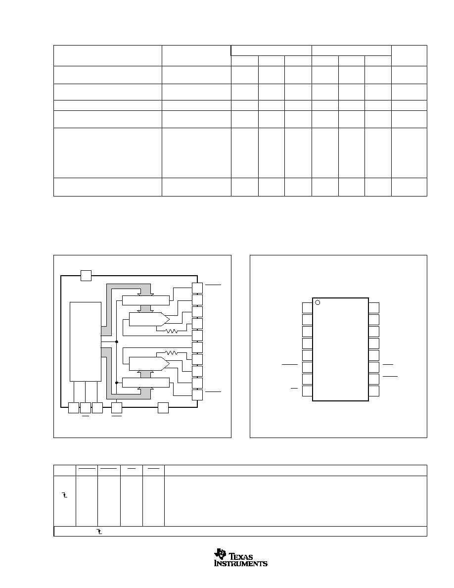
DAC7800
BLOCK DIAGRAM
DAC A
DAC B
DAC A Register
12
12
12
UPD B
I
AGND B
R
V
V
R
I
AGND A
UPD A
OUT B
FB B
REF B
REF A
FB A
OUT A
12
V
DD
9
DGND
10
15
16
14
13
4
3
2
1
6
DAC B Register
Bit 0
Bit 11
Bit 12
Bit 23
Control Logic and Shift Register
7
11
CLR
12
DAC7800
Data
In
5
CLK
8
CS
PIN CONFIGURATION
1
2
3
4
5
6
7
8
16
15
14
13
12
11
10
9
AGND A
CLK
UPD A
Data In
CS
AGND B
I
R
V
V
CLR
UPD B
DGND
OUT A
FB A
REF A
OUT B
DAC7800
I
R
V
FB B
REF B
DD
CLK
UPD A
UPD B
CS
CLR
FUNCTION
X
X
X
X
0
All register contents set to 0's (asynchronous).
X
X
X
1
X
No data transfer.
X
X
0
1
Input data is clocked into input register (location Bit 23) and previous data shifts.
X
0
1
0
1
Input register bits 23 (LSB) - 12 (MSB) are loaded into DAC A.
X
1
0
0
1
Input register bits 11 (LSB) - 0 (MSB) are loaded into DAC B.
X
0
0
0
1
Input register bits 23 (LSB) - 12 (MSB) are loaded into DAC A, and input register bits 11 (LSB) - 0 (MSB)
are loaded into DAC B.
X = Don't care.
means falling edge triggered.
LOGIC TRUTH TABLE
Top View
DIP
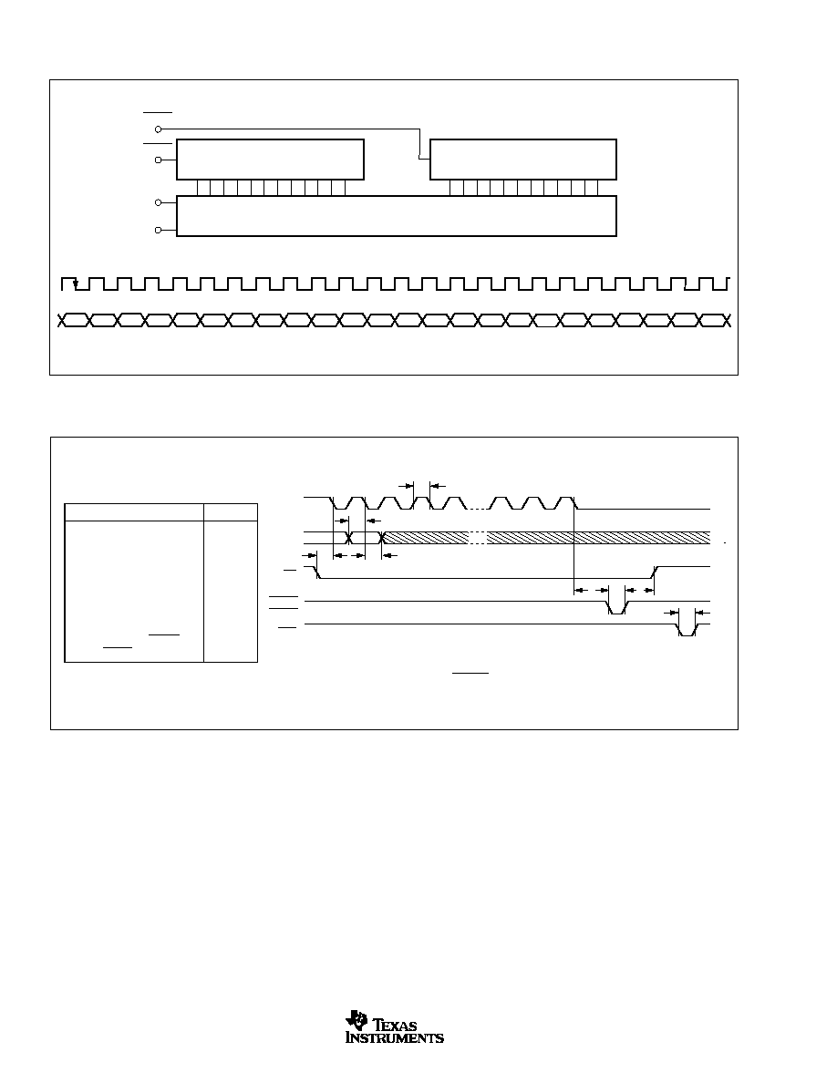
DAC7800, 7801, 7802
4
SBAS005A
www.ti.com
DATA
CS
CLK
t
1
t
5
UPD A
UPD B
t
3
t
7
CLR
t
6
t
8
t
4
0V
5V
5V
5V
5V
0V
NOTES: (1) All input signal rise and fall times are measured from 10% to 90% of +5V. t = t = 5ns.
(2) Timing measurement reference level is V + V
2
F
R
IH
IL
.
t
2
PARAMETER
MINIMUM
t
1
-- Data Setup Time
15ns
t
2
-- Data Hold Time
15ns
t
3
-- Chip Select to CLK,
15ns
Update, Data Setup Time
t
4
-- Chip Select to CLK,
40ns
Update, Data Hold Time
t
5
-- CLK Pulse Width
40ns
t
6
-- Clear Pulse Width
40ns
t
7
-- Update Pulse Width
40ns
t
8
-- CLK Edge to UPD A
15ns
or UPD B
TIMING CHARACTERISTICS
V
DD
= +5V, V
REF A
= V
REF B
= +10V, T
A
= ≠40
∞
C to +85
∞
C.
Data In
Bit 0
Bit 23
Bit 22
Bit 21
Bit 20
Bit 19
Bit 18
Bit 17
Bit 16
Bit 15
Bit 14
Bit 13
Bit 12
Bit 11
Bit 10
Bit 9
Bit 8
Bit 7
Bit 6
Bit 5
Bit 4
Bit 3
Bit 2
Bit 1
LSB
DAC A
MSB
DAC A
LSB
DAC B
MSB
DAC B
DAC7800 Data Input Sequence
DAC7800 Digital Interface Block Diagram
24-Bit
Shift Register
DAC A Register
UPD A
Data In
CLK
UPD B
LSB
MSB
DAC B Register
LSB
MSB
Bit
23
Bit
12
Bit
11
Bit
0
CLK
DATA INPUT FORMAT
DAC7800
(Cont.)
DAC7800, 7801, 7802
5
SBAS005A
www.ti.com
LOGIC TRUTH TABLE
BLOCK DIAGRAM
PIN CONFIGURATION
1
2
3
4
5
6
7
8
9
10
11
12
24
23
22
21
20
19
18
17
16
15
14
13
AGND A
CS
DB0
DB1
DB2
DB3
DB4
DB5
DGND
AGND B
I
R
V
V
UPD
WR
CLR
A1
A0
DB7
DB6
OUT A
FB A
REF A
FB B
REF B
DD
OUT B
DAC7801
I
R
V
DAC7801
CLR
UPD
CS
WR
A1
A0
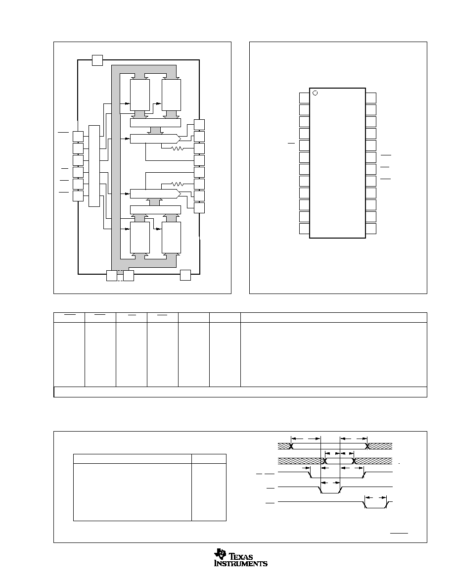
FUNCTION
1
1
1
X
X
X
No Data Transfer
1
1
X
1
X
X
No Data Transfer
0
X
X
X
X
X
All Registers Cleared
1
1
0
0
0
0
DAC A LS Input Register Loaded with DB7 - DB0 (LSB)
1
1
0
0
0
1
DAC A MS Input Register Loaded with DB3 (MSB) - DB0
1
1
0
0
1
0
DAC B LS Input Register Loaded with DB7 - DB0 (LSB)
1
1
0
0
1
1
DAC B MS Input Register Loaded with DB3 (MSB) - DB0
1
0
1
0
X
X
DAC A, DAC B Registers Updated Simultaneously from Input Registers
1
0
0
0
X
X
DAC A, DAC B Registers are Transparent
X = Don't care.
TIMING CHARACTERISTICS
V
DD
= +5V, V
REF A
= V
REF B
= +10V, T
A
= ≠40
∞
C to +85
∞
C.
PARAMETER
MINIMUM
t
1
-- Address Valid to Write Setup Time
10ns
t
2
-- Address Valid to Write Hold Time
10ns
t
3
-- Data Setup Time
30ns
t
4
-- Data Hold Time
10ns
t
5
-- Chip Select or Update to Write Setup Time
0ns
t
6
-- Chip Select or Update to Write Hold Time
0ns
t
7
-- Write Pulse Width
40ns
t
8
-- Clear Pulse Width
40ns
A0≠A1
CLR
t
2
t
1
t
8
WR
t
7
CS, UPD
t
6
t
4
t
3
DATA
t
5
5V
0V
5V
0V
5V
0V
5V
0V
5V
0V
NOTES: (1) All input signal rise and fall times are measured from 10% to 90%
of +5V. t
R
= t
F
= 5ns. (2) Timing measurement reference level is .
V
IH
+ V
IL
2
DAC A
I
AGND A
R
V
V
R
I
AGND B
OUT A
FB A
REF A
REF B
FB B
OUT B
20
V
DD
2
1
3
4
21
22
23
24
DAC A Register
4
8
DAC A
LS
Input
Reg
DAC A
MS
Input
Reg
Control Logic
DAC B
DAC B Register
4
8
12
DGND
DAC B
LS
Input
Reg
DAC B
MS
Input
Reg
19
16
15
5
18
17
UPD
A1
A0
CS
WR
CLR
DAC7801
14
6
DB7≠DB0
12
12
Top View
DIP
DAC7800, 7801, 7802
6
SBAS005A
www.ti.com
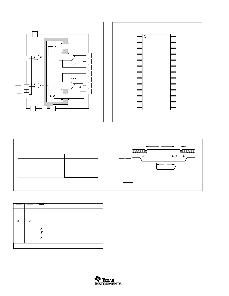
BLOCK DIAGRAM
1
2
3
4
5
6
7
8
9
10
11
12
24
23
22
21
20
19
18
17
16
15
14
13
AGND
I
R
V
CS A
(LSB) DB0
DB1
DB2
DB3
DB4
DB5
DGND
I
R
V
V
CS B
WR
DB11 (MSB)
DB10
DB9
DB8
DB7
DB6
OUT A
FB A
REF A
FB B
REF B
DD
OUT B
DAC7802
TIMING CHARACTERISTICS
At V
DD
= +5V, and T
A
= ≠40
o
C to +85
o
C.
PARAMETER
MINIMUM
t
1
- Data Setup Time
20ns
t
2
- Data Hold Time
15ns
t
3
- Chip Select to Write Setup Time
30ns
t
4
- Chip Select to Write Hold Time
0ns
t
5
- Write Pulse Width
30ns
LOGIC TRUTH TABLE
CSA
CSB
WR
FUNCTION
X
X
1
No Data Transfer
1
1
X
No Data Transfer
0
A Rising Edge on CSA or CSB Loads
Data to the Respective DAC
0
1
DAC A Register Loaded from Data Bus
1
0
DAC B Register Loaded from Data Bus
0
0
DAC A and DAC B Registers Loaded
from Data Bus
X = Don't care.
means rising edge triggered.
PIN CONFIGURATION
DAC7802
DATA
5V
0V
5V
5V
CSA, CSB
WR
t
2
t
1
t
3
t
4
t
5
NOTES: (1) All input signal rise and fall times are measured from 10%
to 90% of +5V. t
R
= t
R
= 5ns. (2) Timing measurement reference level
is
V
IH
+ V
IL
2
.
CK
DAC B
DAC A
12
12
12
12
12
DGND
18
CS A
5
CS B
20
WR
19
21
V
DD
DAC7802
6
2 I
3 R
OUT A
FB A
23 R
24 I
1 AGND
FB B
OUT B
DAC A Register
CK
DAC B Register
DB11≠DB0
4
22
V
V
REF A
REF B
Top View
DIP
DAC7800, 7801, 7802
7
SBAS005A
www.ti.com
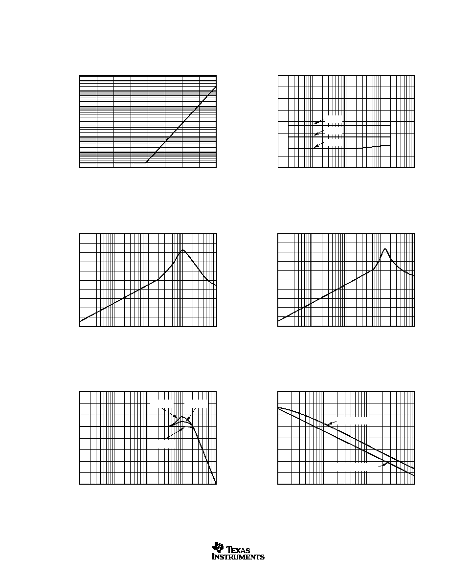
TYPICAL CHARACTERISTICS
OUTPUT OP AMP IS OPA602.
T
A
= +25
∞
C, V
DD
= +5V.
Output Leakage Current (A)
OUTPUT LEAKAGE CURRENT
vs TEMPERATURE
1µ
100n
10n
1n
100p
10p
1p
≠75
≠50
≠25
0
+25
+50
+75
+100
+125
Temperature (∞C)
≠60
≠65
≠70
≠75
≠80
≠85
≠90
≠95
≠100
THD + Noise (dB)
THD + NOISE vs FREQUENCY
Frequency (Hz)
1k
10
100
10k
100k
1Vrms
3Vrms
6Vrms
≠20
≠30
≠40
≠50
≠60
≠70
≠80
≠90
≠100
≠110
≠120
Crosstalk (dB)
CHANNEL-TO-CHANNEL ISOLATION
vs FREQUENCY
Frequency (Hz)
100k
1k
10k
1M
10M
0
≠10
≠20
≠30
≠40
≠50
≠60
≠70
≠80
≠90
≠100
Feedthrough (dB)
FEEDTHROUGH vs FREQUENCY
Frequency (Hz)
100k
1k
10k
1M
10M
+30
+20
+10
0
≠10
≠20
≠30
≠40
≠50
Gain (dB)
FREQUENCY RESPONSE
Frequency (Hz)
100k
1k
10k
1M
10M
C
F
= 5pF
C
F
= 10pF
C
F
= 0pF
Frequency (Hz)
PSRR (dB)
PSRR vs FREQUENCY
70
60
50
40
30
20
10
0
≠10
1k
10k
100k
1M
DAC Loaded w/0s
DAC Loaded w/1s
DAC7800, 7801, 7802
8
SBAS005A
www.ti.com
DISCUSSION OF
SPECIFICATIONS
RELATIVE ACCURACY
This term, also known as end point linearity or integral
linearity, describes the transfer function of analog output to
digital input code. Relative accuracy describes the deviation
from a straight line, after zero and full-scale errors have been
adjusted to zero.
DIFFERENTIAL NONLINEARITY
Differential nonlinearity is the deviation from an ideal 1LSB
change in the output when the input code changes by 1LSB.
A differential nonlinearity specification of 1LSB maximum
ensures monotonicity.
GAIN ERROR
Gain error is the difference between the full-scale DAC output
and the ideal value. The ideal full scale output value for the
DAC780x is ≠(4095/4096)V
REF
. Gain error may be adjusted
to zero using external trims, see Figures 5 and 7.
OUTPUT LEAKAGE CURRENT
The current which appears at I
OUT A
and I
OUT B
with the DAC
loaded with all zeros.
OUTPUT CAPACITANCE
The parasitic capacitance measured from I
OUT A
or I
OUT B
to
AGND.
CHANNEL-TO-CHANNEL ISOLATION
The AC output error due to capacitive coupling from DAC A
to DAC B or DAC B to DAC A.
MULTIPLYING FEEDTHROUGH ERROR
The AC output error due to capacitive coupling from V
REF
to
I
OUT
with the DAC loaded with all zeros.
OUTPUT CURRENT SETTLING TIME
The time required for the output current to settle to within
+0.01% of final value for a full-scale step.
DIGITAL-TO-ANALOG GLITCH ENERGY
The integrated area of the glitch pulse measured in nanovolt-
seconds. The key contributor to DAC glitch is charge injected
by digital logic switching transients.
DIGITAL CROSSTALK
Glitch impulse measured at the output of one DAC but caused
by a full-scale transition on the other DAC. The integrated
area of the glitch pulse is measured in nanovolt-seconds.
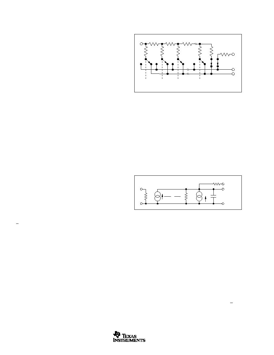
CIRCUIT DESCRIPTION
Figure 1 shows a simplified schematic of one half of a DAC780x.
The current from the V
REF
A
pin is switched between I
OUT A
and
AGND by 12 single-pole double-throw CMOS switches. This
maintains a constant current in each leg of the ladder regard-
less of the input code. The input resistance at V
REF
is therefore
A CMOS switch transistor, included in series with the ladder
terminating resistor and in series with the feedback resistor,
R
FB A
, compensates for the temperature drift of the ON resis-
tance of the ladder switches.
Figure 2 shows an equivalent circuit for DAC A. C
OUT
is the
output capacitance due to the N-channel switches and varies
from about 30pF to 70pF with digital input code. The current
source I
LKG
is the combination of surface and junction leak-
ages to the substrate. I
LKG
approximately doubles every 10
∞
C.
R
O
is the equivalent output resistance of the DAC and it varies
with input code.
constant and can be driven by either a voltage or current, AC
or DC, positive or negative polarity, and have a voltage range
up to
±
20V.
OUT A
I
AGND
FB A
R
2R
2R
2R
2R
2R
R
R
R
V
REF A
DB11
(MSB)
DB10
DB9
DB0
(LSB)
R
FIGURE 1. Simplified Circuit Diagram for DAC A.
FIGURE 2. Equivalent Circuit for DAC A.
FB A
R
OUT A
I
V
REF A
I
LKG
R
OUT
C
O
R
AGND A
D
IN
4096
x
V
REF
R
R
INSTALLATION
ESD PROTECTION
All digital inputs of the DAC780x incorporate on-chip ESD
protection circuitry. This protection is designed to withstand
2.5kV (using the Human Body Model, 100pF and 1500
).
However, industry standard ESD protection methods should
be used when handling or storing these components. When
not in use, devices should be stored in conductive foam or
rails. The foam or rails should be discharged to the destina-
tion socket potential before devices are removed.
POWER-SUPPLY CONNECTIONS
The DAC780x are designed to operate on V
DD
= +5V +10%.
For optimum performance and noise rejection, power-supply
decoupling capacitors C
D
should be added as shown in the
application circuits. These capacitors (1
µ
F tantalum recom-
mended) should be located close to the DAC. AGND and
DAC7800, 7801, 7802
9
SBAS005A
www.ti.com
DGND should be connected together at one point only,
preferably at the power-supply ground point. Separate re-
turns minimize current flow in low-level signal paths if properly
connected. Output op amp analog common (+ input) should
be connected as near to the AGND pins of the DAC780x as
possible.
WIRING PRECAUTIONS
To minimize AC feedthrough when designing a PC board,
care should be taken to minimize capacitive coupling be-
tween the V
REF
lines and the I
OUT
lines. Similarly, capacitive
coupling between DACs may compromise the channel-to-
channel isolation. Coupling from any of the digital control or
data lines might degrade the glitch and digital crosstalk
performance. Solder the DAC780x directly into the PC board
without a socket. Sockets add parasitic capacitance (which
can degrade AC performance).
AMPLIFIER OFFSET VOLTAGE
The output amplifier used with the DAC780x should have low
input offset voltage to preserve the transfer function linearity.
The voltage output of the amplifier has an error component
which is the offset voltage of the op amp multiplied by
the "noise gain" of the circuit. This "noise gain" is equal to
(R
F
/ R
O
+ 1) where R
O
is the output impedance of the DAC
I
OUT
terminal and R
F
is the feedback network impedance. The
nonlinearity occurs due to the output impedance varying with
code. If the 0 code case is excluded (where R
O
= infinity), the
R
O
will vary from R-3R providing a "noise gain" variation
between 4/3 and 2. In addition, the variation of R
O
is nonlinear
with code, and the largest steps in R
O
occur at major code
transitions where the worst differential nonlinearity is also
likely to be experienced. The nonlinearity seen at the amplifier
output is 2V
OS
≠ 4V
OS
/ 3 = 2V
OS
/3. Thus, to maintain good
nonlinearity the op amp offset should be much less than
1/2 LSB.
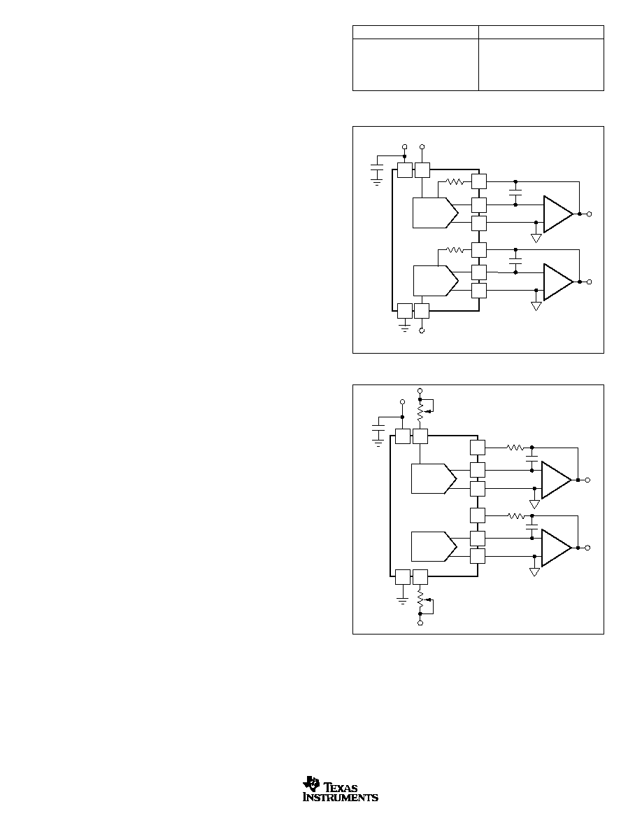
UNIPOLAR CONFIGURATION
Figure 3 shows DAC780x in a typical unipolar (two-quadrant)
multiplying configuration. The analog output values versus
digital input code are listed in Table II. The operational
amplifiers used in this circuit can be single amplifiers such as
the OPA602, or a dual amplifier such as the OPA2107. C1
and C2 provide phase compensation to minimize settling time
and overshoot when using a high speed operational amplifier.
If an application requires the DAC to have zero gain error, the
circuit shown in Figure 4 may be used. Resistors R
2
and R
4
induce a positive gain error greater than worst-case initial
negative gain error. Trim resistors R
1
and R
3
provide a
variable negative gain error and have sufficient trim range to
correct for the worst-case initial positive gain error plus the
error produced by R
2
and R
4
.
BIPOLAR CONFIGURATION
See Figure 5 for the DAC780x in a typical bipolar (four-
quadrant) multiplying configuration. See Table III for the
listing of the analog output values versus digital input code.
DATA INPUT
ANALOG OUTPUT
MSB
LSB
1111 1111 1111
≠V
REF
(4095/4096)
1000 0000 0000
≠V
REF
(2048/4096) = ≠1/2V
REF
0000 0000 0001
≠V
REF
(1/4096)
0000 0000 0000
0 Volts
TABLE II. Unipolar Output Code.
The operational amplifiers used in this circuit can be single
amplifiers such as the OPA602, a dual amplifier such as the
OPA2107, or a quad amplifier like the OPA404. C1 and C2
provide phase compensation to minimize settling time and
overshoot when using a high speed operational amplifier. The
bipolar offset resistors R
5
≠R
7
and R
8
≠R
10
should be ratio-
matched to 0.01% to ensure the specified gain error perfor-
mance.
DAC A
I
OUT A
DAC B
AGND A
I
OUT B
R
FB B
R
FB A
C1
10pF
C2
10pF
DAC780X
V
OUT A
V
OUT B
≠
+
≠
+
A1
A2
DGND
V
REF B
V
REF A
V
DD
+5V
C
D
A1, A2 OPA602 or 1/2 OPA2107.
DAC7802 has a single analog
common, AGND.
+
1µF
AGND B
R
100
3
REF B
R
2
47
R
4
47
DAC A
I
OUT A
DAC B
AGND A
I
OUT B
R
FB B
R
FB A
C1 10pF
C2 10pF
DAC780X
V
OUT A
V
OUT B
≠
+
≠
+
A1
A2
DGND
V
DD
+5V
C
D
A1, A2 OPA602 or 1/2 OPA2107.
DAC7802 has a single analog
common, AGND.
+
1µF
AGND B
V
IN A
R
100
1
REF A
V
V
IN B
V
FIGURE 4. Unipolar Configuration with Gain Trim.
FIGURE 3. Unipolar Configuration.
DAC7800, 7801, 7802
10
SBAS005A
www.ti.com
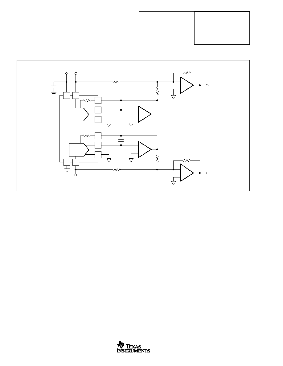
If an application requires the DAC to have zero gain error, the
circuit may be used, see Figure 6. Resistors R
2
and R
4
induce
a positive gain error greater than worst-case initial negative
gain error. Trim resistors R
1
and R
3
provide a variable
negative gain error and have sufficient trim range to correct
for the worst-case initial positive gain error plus the error
produced by R
2
and R
4
.
DATA INPUT
ANALOG OUTPUT
MSB
LSB
1111 1111 1111
+V
REF
(2047/2048)
1000 0000 0001
+V
REF
(1/2048)
1000 0000 0000
0 Volts
0111 1111 1111
≠V
REF
(1/2048)
0000 0000 0000
≠V
REF
(2048/2048)
TABLE III. Bipolar Output Code.
FIGURE 5. Bipolar Configuration.
R
3
10k
1
C
10pF
DAC A
DAC B
R
10k
5
DAC780X
DGND
V
REF A
V
DD
+5V
C
D
2
R
6
20k
R
2
20k
R
10k
C
10pF
V
OUT A
V
OUT B
A1
A3
DAC7802 has a single analog common, AGND.
A1≠A4, OPA602 or 1/2 OPA2107.
≠
+
A2
≠
+
A4
5
R
1
20k
R
4
20k
REF B
V
I
OUT B
R
FB B
≠
+
AGND B
I
OUT A
R
FB A
≠
+
AGND A
1µF
+
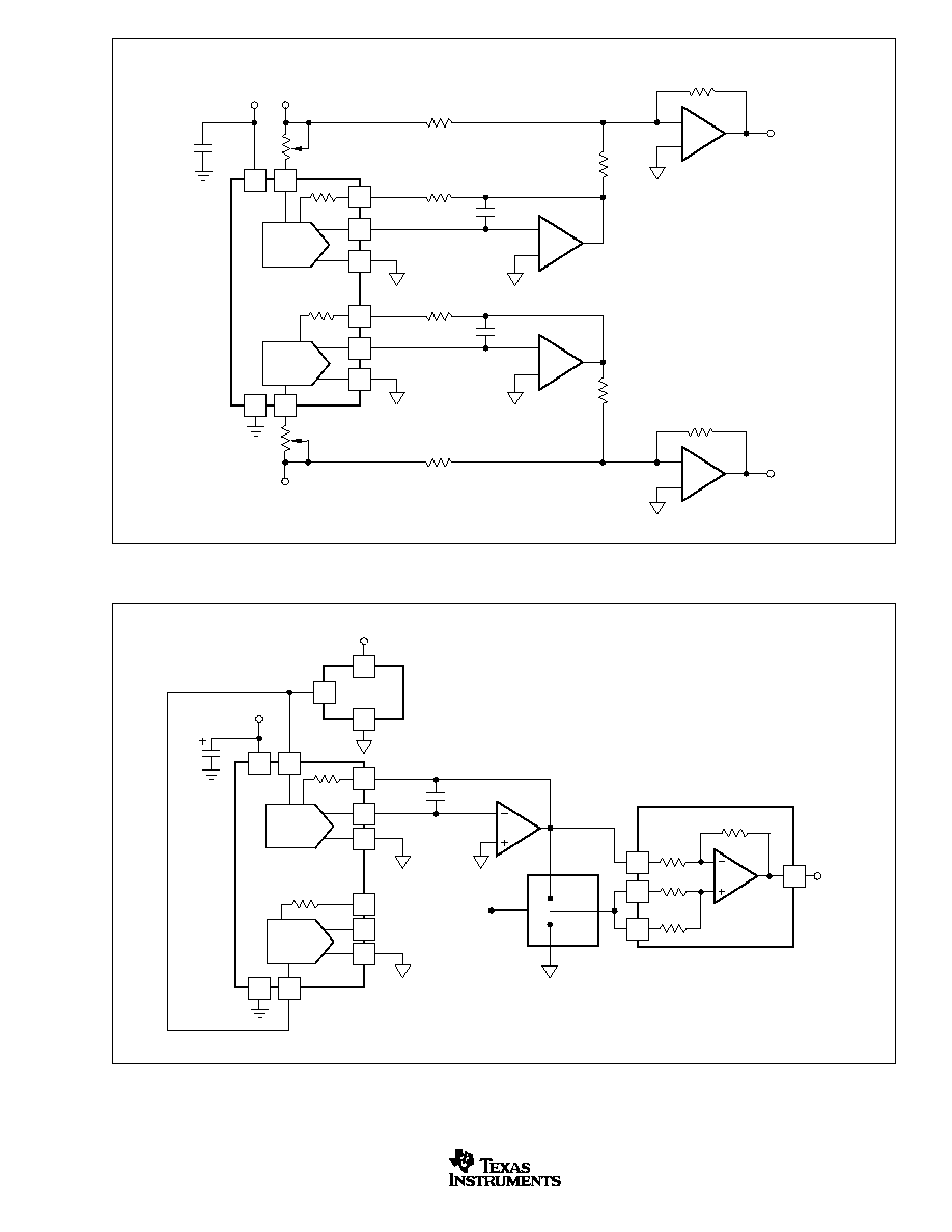
APPLICATIONS
12-BIT PLUS SIGN DACS
For a bipolar DAC with 13 bits of resolution, two solutions are
possible. The addition of a precision difference amplifier and
a high speed JFET switch provides a 12-bit plus sign voltage-
output DAC, see Figure 7. When the switch selects the op
amp output, the difference amplifier serves as a noninverting
output buffer. If the analog ground side of the switch is
selected, the output of the difference amplifier is inverted.
Another option, see Figure 8, also produces a 12-bit plus sign
output without the additional switch and digital control line.
DIGITALLY PROGRAMMABLE ACTIVE FILTER
See Figure 9 for the DAC780x in a digitally programmable
active filter application. The design is based on the state-
variable filter, Texas Instruments UAF42, an active filter topol-
ogy that offers stable and repeatable filter characteristics.
DAC1 and DAC2 can be updated in parallel with a single word
to set the center frequency of the filter. DAC 4, which makes
use of the uncommitted op amp in UAF42, sets the Q of the
filter. DAC3 sets the gain of the filter transfer function without
changing the Q of the filter. The reverse is also true.
The center frequency is determined by f
C
= 1/2
RC where R is
the ladder resistance of the DAC (typical value, 10k
) and C
the internal capacitor value (1000pF) of the UAF42. External
capacitors can be added to lower the center frequency of the
filter. But the highest center frequency for this circuit will be
about 16kHz because the effective series resistance of the
DAC cannot be less than 10k
.
Note that the ladder resistance of the DAC may vary from
device to device. Thus, for best tracking, DAC2 and DAC3
should be in the same package. Some calibration may be
necessary from one filter to another.
DAC7800, 7801, 7802
11
SBAS005A
www.ti.com
FIGURE 6. Bipolar Configuration with Gain Trim.
R
100
1
R
7
10k
1
C
10pF
DAC A
DAC B
R
10k
DAC7802
DGND
V
IN A
V
DD
+5V
C
D
2
R
10
20k
R
6
20k
R
10k
C
10pF
V
OUT A
V
OUT B
A1
A3
DAC7802 has a single analog common, AGND.
A1≠A4, OPA602 or 1/2 OPA2107.
≠
+
A2
≠
+
A4
9
R
5
20k
R
8
20k
V
I
OUT B
R
FB B
≠
+
AGND B
I
OUT A
R
FB A
≠
+
AGND A
R
100
3
R
2
47
R
4
47
IN B
+
1µF
V
REF A
V
REF B
FIGURE 7. 12-Bit Plus Sign DAC.
1
C
10pF
I
OUT A
DAC A
DAC B
R
FB A
DAC780X
DGND
V
DD
+5V
C
D
A1
DAC7802 has a single analog common, AGND.
A1 OPA602 or 1/2 OPA2107.
INA105
DG188
Sign Control
REF102
±10V
13 Bits
V
REF B
+15V
V
REF A
R
R
R
R
AGND B
+10V
AGND A
2
4
6
1µF
2
3
1
6

DAC7800, 7801, 7802
12
SBAS005A
www.ti.com
FIGURE 8. 13-Bit Bipolar DAC.
1
C
10pF
I
OUT A
DAC A
DAC B
R
FB A
DAC780X
DGND
V
DD
+5V
A1
DAC7802 has a single analog common, AGND.
A1 OPA602 or 1/2 OPA2107.
REF102
±10V
13 Bits
V
REF B
+15V
V
REF A
R
R
R
AGND B
AGND A
+10V
I
OUT B
R
FB B
2
C
10pF
A2
R
C
D
INA105
2
4
6
1µF
2
3
6
1
V
REF 2
DAC 2
DAC 1
DAC 3
Gain Adjust
Filter Input
V
REF 3
I
OUT 3
AGND 3
High-Pass Out
Band-Pass
Out
Low-Pass
Out
UAF 42
C
C
R
R
R
R
DAC780X
V
REF 1
I
OUT 1
AGND 1
I
OUT 2
AGND 2
DAC 4
Q Adjust
V
REF 4
I
OUT 4
AGND 4
R
FB 4
C
Adjust
f
R = 50k
C = 1000pF ±0.5%
±0.5%
1/2 DAC780X
1/2 DAC780X
1
5
13
12
3
14
7
2
11
8
4
6
FIGURE 9. Digitally Programmable Universal Active Filter.
DAC7800, 7801, 7802
13
SBAS005A
www.ti.com
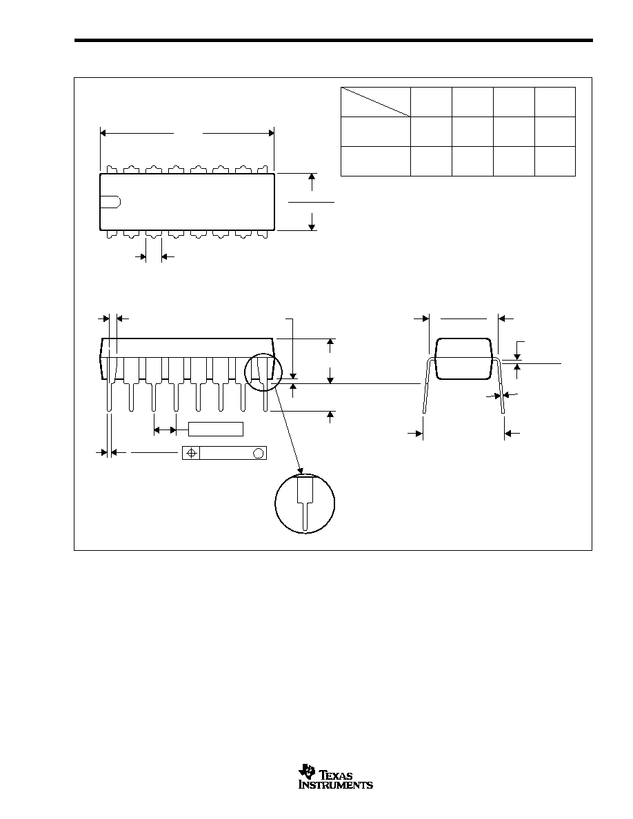
PACKAGE DRAWINGS
MPDI002B ≠ JANUARY 1995 ≠ REVISED FEBRUARY 2000
N (R-PDIP-T**)
PLASTIC DUAL-IN-LINE PACKAGE
0.325 (8,26)
0.300 (7,62)
0.010 (0,25) NOM
Gauge Plane
0.015 (0,38)
0.430 (10,92) MAX
20
0.975
(24,77)
0.940
(23,88)
18
0.920
0.850
14
0.775
0.745
(19,69)
(18,92)
16
0.775
(19,69)
(18,92)
0.745
A MIN
DIM
A MAX
PINS **
(23,37)
(21,59)
Seating Plane
14/18 PIN ONLY
4040049/D 02/00
9
8
0.070 (1,78) MAX
A
0.035 (0,89) MAX
0.020 (0,51) MIN
16
1
0.015 (0,38)
0.021 (0,53)
0.200 (5,08) MAX
0.125 (3,18) MIN
0.240 (6,10)
0.260 (6,60)
M
0.010 (0,25)
0.100 (2,54)
16 PINS SHOWN
NOTES: A. All linear dimensions are in inches (millimeters).
B. This drawing is subject to change without notice.
C. Falls within JEDEC MS-001 (20-pin package is shorter than MS-001).
DAC7800, 7801, 7802
14
SBAS005A
www.ti.com
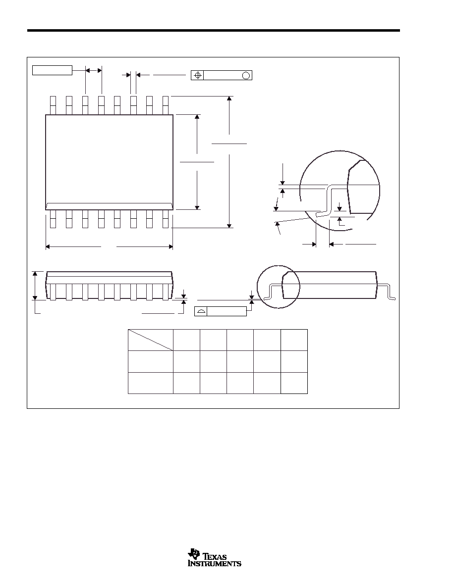
PACKAGE DRAWINGS (Cont)
MSOI003E ≠ JANUARY 1995 ≠ REVISED SEPTEMBER 2001
DW (R-PDSO-G**)
PLASTIC SMALL-OUTLINE PACKAGE
16 PINS SHOWN
4040000 / E 08/01
Seating Plane
0.400 (10,15)
0.419 (10,65)
0.104 (2,65) MAX
1
0.012 (0,30)
0.004 (0,10)
A
8
16
0.020 (0,51)
0.014 (0,35)
0.291 (7,39)
0.299 (7,59)
9
0.010 (0,25)
0.050 (1,27)
0.016 (0,40)
(15,24)
(15,49)
PINS **
0.010 (0,25) NOM
A MAX
DIM
A MIN
Gage Plane
20
0.500
(12,70)
(12,95)
0.510
(10,16)
(10,41)
0.400
0.410
16
0.600
24
0.610
(17,78)
28
0.700
(18,03)
0.710
0.004 (0,10)
M
0.010 (0,25)
0.050 (1,27)
0 Ò8
(11,51)
(11,73)
0.453
0.462
18
NOTES: A. All linear dimensions are in inches (millimeters).
B. This drawing is subject to change without notice.
C. Body dimensions do not include mold flash or protrusion not to exceed 0.006 (0,15).
D. Falls within JEDEC MS-013

DAC7800, 7801, 7802
15
SBAS005A
www.ti.com
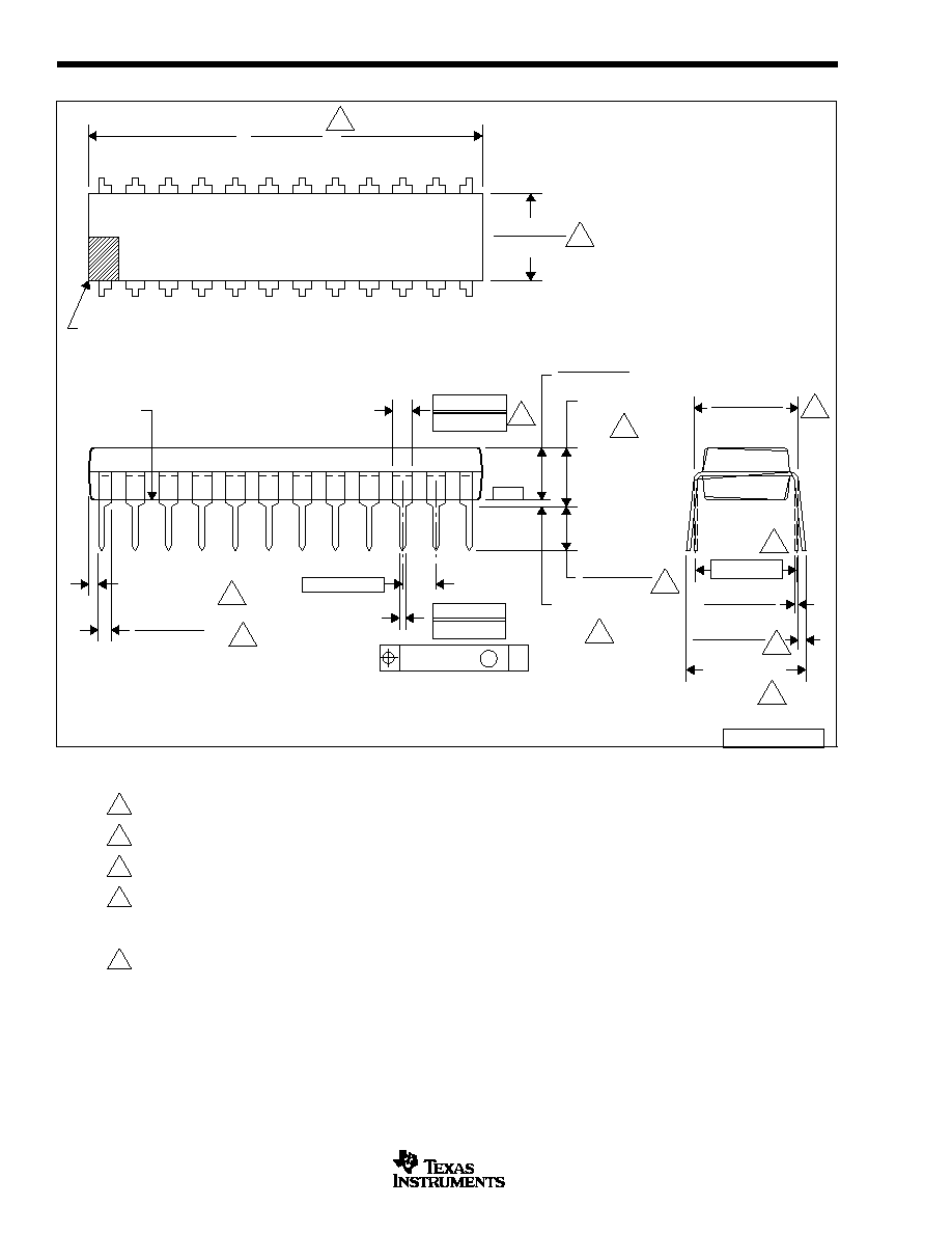
PACKAGE DRAWINGS (Cont)
MPDI004 ≠ OCTOBER 1994
NT (R-PDIP-T**)
PLASTIC DUAL-IN-LINE PACKAGE
4040050 / B 04/95
24 PINS SHOWN
1.425
(36,20)
1.385
0.295
(7,49)
(8,00)
0.315
(35,18)
28
PINS **
A MIN
A MAX
B MAX
B MIN
13
0.250 (6,35)
0.280 (7,11)
12
0.200 (5,08) MAX
DIM
24
1.230
(31,24)
(32,04)
1.260
0.310
(7,87)
(7,37)
0.290
B
0.125 (3,18) MIN
Seating Plane
0.010 (0,25) NOM
A
0.070 (1,78) MAX
24
1
0.015 (0,38)
0.021 (0,53)
0.020 (0,51) MIN
0.100 (2,54)
M
0.010 (0,25)
0
∞
≠ 15
∞
NOTES: A. All linear dimensions are in inches (millimeters).
B. This drawing is subject to change without notice.
DAC7800, 7801, 7802
16
SBAS005A
www.ti.com
PACKAGE DRAWINGS (Cont)
MPDI066 ≠ AUGUST 2001
NTG (R-PDIP-T24)
PLASTIC DUAL-IN-LINE
4202642/A 08/01
0.150 (3,81)
0.115 (2,92)
≠C≠
0.005 (0,13) MIN
1/2 Lead 4 PL
1
1
2
13
24
1.195 (30,35)
1.160 (29,46)
0.240 (6,10)
0.280 (7,11)
0.070 (1,78)
0.045 (1,14)
0.030 (0,76)
0.045 (1,14)
0.014 (0,36)
0.022 (0,56)
0.010 (0,25) M
C
0.210 (5,33)
0.195 (4,95)
0.115 (2,92)
0.300 (7,62)
MAX
0.430 (10,92)
0.000 (0,00)
0.060 (1,52)
0.014 (0,36)
0.008 (0,20)
0.325 (8,26)
0.300 (7,62)
Index
Area
0.015 (0,38)
MIN
0.100 (2,54)
Seating Plane
Base Plane
MAX
C
C
C
E
F
F
D
D
H
H
D
E
4 PL
NOTES: A. All linear dimensions are in inches (millimeters).
B. This drawing is subject to change without notice.
C. Dimensions are measured with the package
seated in JEDEC seating plane gauge GS-3.
D. Dimensions do not include mold flash or protrusions.
Mold flash or protrusions shall not exceed 0.010 (0,25).
E. Dimensions measured with the leads constrained to be
perpendicular to Datum C.
F. Dimensions are measured at the lead tips with the
leads unconstrained.
G. Pointed or rounded lead tips are preferred to ease
insertion.
H. Maximum dimensions do not include dambar
protrusions. Dambar protrusions shall not exceed
0.010 (0,25).
I. Distance between leads including dambar protrusions
to be 0.005 (0,13) minumum.
J. A visual index feature must be located within the
cross≠hatched area.
K. For automatic insertion, any raised irregularity on the
top surface (step, mesa, etc.) shall be symmetrical
about the lateral and longitudinal package centerlines.
L. Controlling dimension in inches.
M. Falls within JEDEC MS-011-AB.

IMPORTANT NOTICE
Texas Instruments Incorporated and its subsidiaries (TI) reserve the right to make corrections, modifications,
enhancements, improvements, and other changes to its products and services at any time and to discontinue
any product or service without notice. Customers should obtain the latest relevant information before placing
orders and should verify that such information is current and complete. All products are sold subject to TI's terms
and conditions of sale supplied at the time of order acknowledgment.
TI warrants performance of its hardware products to the specifications applicable at the time of sale in
accordance with TI's standard warranty. Testing and other quality control techniques are used to the extent TI
deems necessary to support this warranty. Except where mandated by government requirements, testing of all
parameters of each product is not necessarily performed.
TI assumes no liability for applications assistance or customer product design. Customers are responsible for
their products and applications using TI components. To minimize the risks associated with customer products
and applications, customers should provide adequate design and operating safeguards.
TI does not warrant or represent that any license, either express or implied, is granted under any TI patent right,
copyright, mask work right, or other TI intellectual property right relating to any combination, machine, or process
in which TI products or services are used. Information published by TI regarding third≠party products or services
does not constitute a license from TI to use such products or services or a warranty or endorsement thereof.
Use of such information may require a license from a third party under the patents or other intellectual property
of the third party, or a license from TI under the patents or other intellectual property of TI.
Reproduction of information in TI data books or data sheets is permissible only if reproduction is without
alteration and is accompanied by all associated warranties, conditions, limitations, and notices. Reproduction
of this information with alteration is an unfair and deceptive business practice. TI is not responsible or liable for
such altered documentation.
Resale of TI products or services with statements different from or beyond the parameters stated by TI for that
product or service voids all express and any implied warranties for the associated TI product or service and
is an unfair and deceptive business practice. TI is not responsible or liable for any such statements.
Mailing Address:
Texas Instruments
Post Office Box 655303
Dallas, Texas 75265
Copyright
2001, Texas Instruments Incorporated