 | –≠–ª–µ–∫—Ç—Ä–æ–Ω–Ω—ã–π –∫–æ–º–ø–æ–Ω–µ–Ω—Ç: DAC7811 | –°–∫–∞—á–∞—Ç—å:  PDF PDF  ZIP ZIP |
www.ti.com
PRODUCT PREVIEW
FEATURES
DESCRIPTION
APPLICATIONS
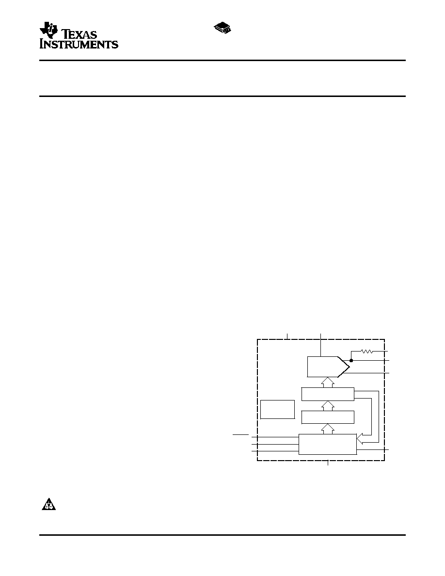
12-Bit
R-2R DAC
DAC Register
Input Latch
Control Logic and
Input Shift Register
Power-On
Reset
DAC7811
R
SYNC
SCLK
SDIN
V
DD
V
REF
R
FB
I
OUT
1
I
OUT
2
SDO
GND
DAC7811
SBAS337 ≠ APRIL 2005
12-Bit, Serial Input, Multiplying
Digital-to-Analog Converter
∑
2.7 V to 5.5 V Supply Operation
The DAC7811 is a CMOS 12-bit current output
digital-to-analog
converter
(DAC).
This
device
∑
50 MHz Serial Interface
operates from a 3.0 V to 5.5 V power supply, making
∑
10 MHz Multiplying Bandwidth
it suitable to both battery-powered and many other
∑
±
10 V Reference Input
applications.
∑
Low Glitch Energy: 2 nV-s
This DAC uses a double-buffered 3-wire serial
∑
Extended Temperature Range:
interface
that
is
compatible
with
SPITM,
QSPI,
≠40
∞
C to +125
∞
C
MICROWIRETM, and most DSP interface standards.
In addition, a serial data out pin (SDO) allows for
∑
10-Lead SON Package
daisy-chaining when multiple packages are used.
∑
12-Bit Monotonic
Data readback allows the user to read the contents of
∑
4-Quadrant Multiplication
the DAC register via the SDO pin. On power-up, the
internal shift register and latches are filled with zeroes
∑
Power-On Reset with Brownout Detection
and the DAC outputs are at zero scale.
∑
Daisy-Chain Mode
The DAC7811 offers excellent 4-quadrant multipli-
∑
Readback Function
cation characteristics, with large signal multiplying
∑
Industry-Standard Pin Configuration
bandwidth of 10 MHz. The applied external reference
input voltage (V
REF
) determines the full-scale output
current. An integrated feedback resistor (R
FB
) pro-
∑
Portable Battery-Powered Instruments
vides temperature tracking and full-scale voltage
output
when
combined
with
an
external
cur-
∑
Waveform Generators
rent-to-voltage precision amplifier.
∑
Analog Processing
∑
Programmable Amplifiers and Attenuators
The DAC7811 is available in a 10-lead MSOP pack-
age as well as a small 10-lead SON package.
∑
Digitally Controlled Calibration
∑
Programmable Filters and Oscillators
∑
Composite Video
∑
Ultrasound
Please be aware that an important notice concerning availability, standard warranty, and use in critical applications of Texas
Instruments semiconductor products and disclaimers thereto appears at the end of this data sheet.
SPI is a trademark of Motorola, Inc.
MICROWIRE is a trademark of National Semiconductor.
All trademarks are the property of their respective owners.
PRODUCT PREVIEW information concerns products in the forma-
Copyright © 2005, Texas Instruments Incorporated
tive or design phase of development. Characteristic data and other
specifications are design goals. Texas Instruments reserves the
right to change or discontinue these products without notice.

www.ti.com
PRODUCT PREVIEW
ABSOLUTE MAXIMUM RATINGS
ELECTRICAL CHARACTERISTICS
DAC7811
SBAS337 ≠ APRIL 2005
This integrated circuit can be damaged by ESD. Texas Instruments recommends that all integrated
circuits be handled with appropriate precautions. Failure to observe proper handling and installation
procedures can cause damage.
ESD damage can range from subtle performance degradation to complete device failure. Precision
integrated circuits may be more susceptible to damage because very small parametric changes could
cause the device not to meet its published specifications.
ORDERING INFORMATION
(1)
SPECIFIED
PACKAGE
PACKAGE
ORDERING NUM-
TRANSPORT MEDIA,
PRODUCT
PACKAGE
TEMPERATURE
DESIGNATOR
MARKING
BER
QUANTITY
RANGE
DAC7811
10-MSOP
DGS
≠40
∞
C to +125
∞
C
7811
DAC7811IDGST
250, Tape and Reel
DAC7811IDGSR
2500, Tape and Reel
DAC7811
10-SON
DRC
≠40
∞
C to +125
∞
C
7811
DAC7811IDRCT
250, Tape and Reel
DAC7811IDRCR
2500, Tape and Reel
(1)
For the most current specifications and package information, see the Package Option Addendum located at the end of this data sheet or
refer to our web site at
www.ti.com
.
over operating free-air temperature range (unless otherwise noted)
(1)
DAC7811
UNIT
V
DD
to GND
≠0.3 to +7.0
V
Digital input voltage to GND
≠0.3 to V
DD
+ 0.3
V
V
OUT
to GND
≠0.3 to V
DD
+ 0.3
V
Operating temperature range
≠40 to +125
∞
C
Storage temperature range
≠65 to +150
∞
C
Junction temperature (T
J
max)
+150
∞
C
ESD Rating, HBM
1500
V
ESD Rating, CDM
1000
V
(1)
Stresses above those listed under absolute maximum ratings may cause permanent damage to the device. Exposure to absolute
maximum conditions for extended periods may affect device reliability.
V
DD
= +2.7 V to +5.5 V; I
OUT1
= Virtual GND; I
OUT2
= 0V; V
REF
= 10 V; T
A
= full operating temperature. All specifications ≠40
∞
C
to +125
∞
C, unless otherwise noted.
DAC7811
PARAMETER
CONDITIONS
MIN
TYP
MAX
UNITS
STATIC PERFORMANCE
(1)
Resolution
12
Bits
Relative accuracy
DAC7811
±
1
LSB
Differential nonlinearity
±
1
LSB
Output leakage current
Data = 0000h, T
A
= +25
∞
C
±
5
nA
Output leakage current
Data = 0000h, T
A
= T
MAX
±
25
nA
Full-scale gain error
All ones loaded to DAC register
±
5
±
10
mV
Full-scale tempco
±
5
ppm/
∞
C
Output capacitance
Code dependent
50
pF
(1)
Linearity calculated by using a reduced code range of 48 to 4047; output unloaded.
2
www.ti.com
PRODUCT PREVIEW
DAC7811
SBAS337 ≠ APRIL 2005
ELECTRICAL CHARACTERISTICS (continued)
V
DD
= +2.7 V to +5.5 V; I
OUT1
= Virtual GND; I
OUT2
= 0V; V
REF
= 10 V; T
A
= full operating temperature. All specifications ≠40
∞
C
to +125
∞
C, unless otherwise noted.
DAC7811
PARAMETER
CONDITIONS
MIN
TYP
MAX
UNITS
REFERENCE INPUT
V
REF
range
≠15
15
V
Input resistance
8
10
12
k
R
FB
resistance
8
10
12
k
LOGIC INPUTS AND OUTPUT
(2)
Input low voltage
V
IL
V
DD
= +2.7V
0.6
V
V
IL
V
DD
= +5V
0.8
V
Input high voltage
V
IH
V
DD
= +2.7V
2.1
V
V
IH
V
DD
= +5V
2.4
V
Input leakage current
I
IL
10
µA
Input capacitance
C
IL
10
pF
INTERFACE TIMING
Clock input frequency
f
CLK
50
MHz
Clock pulse width high
t
CH
8
ns
Clock pulse width low
t
CC
8
ns
SYNC falling edge to SCLK
t
CSS
13
ns
active edge setup time
SCLK active edge to SYNC
t
CST
5
ns
rising edge hold time
Data setup time
t
DS
5
ns
Data hold time
t
DH
5
ns
SYNC high time
t
SH
30
V
DD
= +2.7V
25
35
ns
SYNC inactive edge to SDO
t
DDS
valid
V
DD
= +5V
20
30
ns
POWER REQUIREMENTS
V
DD
2.7
5.5
V
I
DD
(normal operation)
Logic inputs = 0 V
5
µA
V
DD
= +4.5 V to +5.5 V
V
IH
= V
DD
and V
IL
= GND
0.8
5
µA
V
DD
= +2.7 V to +3.6 V
V
IH
= V
DD
and V
IL
= GND
0.4
2.5
µA
AC CHARACTERISTICS
Output voltage settling time
0.2
µs
Reference multiplying BW
V
REF
= 7 V
PP
, Data = FFFh
10
MHz
V
REF
= 0 V to 10 V,
DAC glitch impulse
2
nV-s
Data = 7FFh to 800h to 7FFh
Feedthrough error V
OUT
/V
REF
Data = 000h, V
REF
= 100kHz
≠70
dB
Digital feedthrough
2
nV-s
Total harmonic distortion
≠105
dB
Output spot noise voltage
25
nV/
Hz
(2)
Specified by design and characterization; not production tested.
3
www.ti.com
PRODUCT PREVIEW
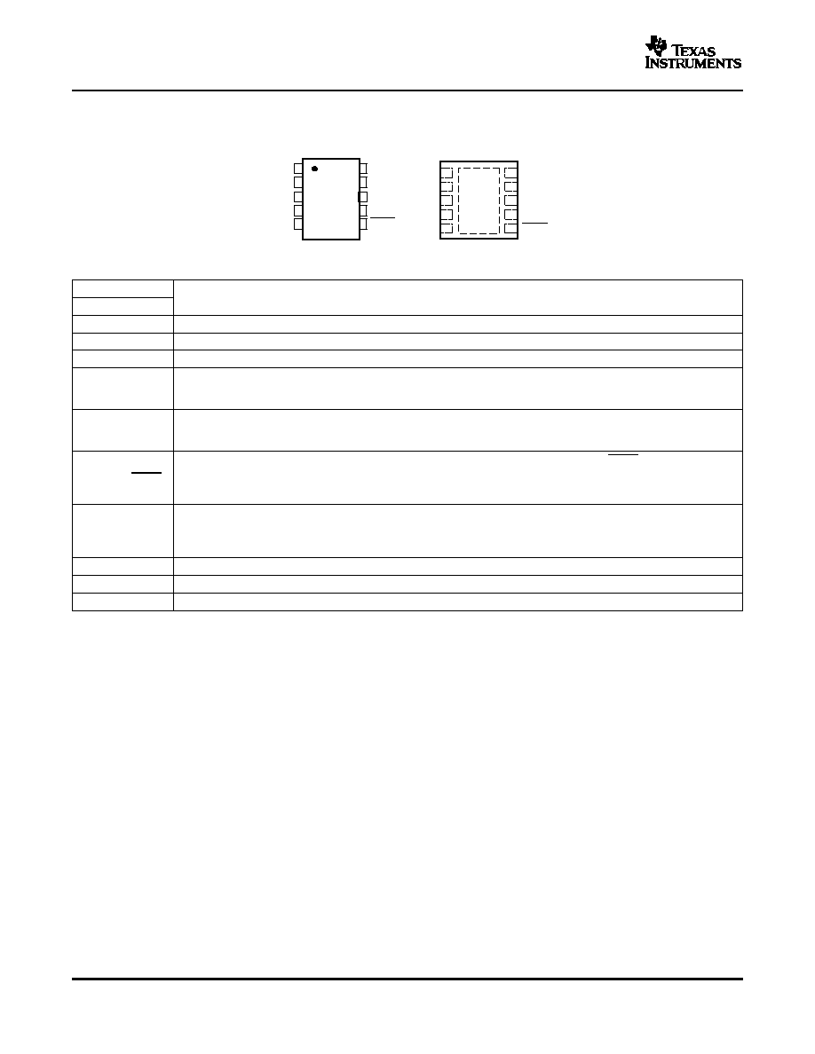
PIN DESCRIPTIONS
MSOP PACKAGE
(TOP VIEW)
1
2
3
4
5
10
9
8
7
6
I
OUT
1
I
OUT
2
GND
SCLK
SDIN
R
FB
V
REF
V
DD
SDO
SYNC
R
FB
V
REF
V
DD
SDO
SYNC
10
9
8
7
6
I
OUT
1
I
OUT
2
GND
SCLK
SDIN
1
2
3
4
5
SON PACKAGE
3mm x 3mm QFN
(TOP VIEW)
DAC7811
SBAS337 ≠ APRIL 2005
Table 1. TERMINAL FUNCTIONS
TERMINAL
DESCRIPTION
NO.
NAME
1
I
OUT
1
DAC Current Output
2
I
OUT
2
DAC Analog Ground. This pin is normally tied to the analog ground of the system.
3
GND
Ground pin.
Serial Clock Input. By default, data is clocked into the input shift register on the falling edge of the serial clock input.
4
SCLK
Alternatively, by means of the serial control bits, the device may be configured such that data is clocked into the shift
register on the rising edge of SCLK.
Serial Data Input. Data is clocked into the 16-bit input register on the active edge of the serial clock input. By default,
5
SDIN
on power-up, data is clocked into the shift register on the falling edge of SCLK. The control bits allow the user to
change the active edge to the rising edge.
Active Low Control Input. This is the frame synchronization signal for the input data. When SYNC goes low, it powers
on the SCLK and DIN buffers, and the input shift register is enabled. Data is loaded to the shift register on the active
6
SYNC
edge of the following clocks (power-on default is falling clock edge). In stand-alone mode, the serial interface counts
the clocks and data is latched to the shift register on the 16th active clock edge.
Serial Data Output. This allows a number of parts to be daisy-chained. By default, data is clocked into the shift register
on the falling edge and out via SDO on the rising edge of SCLK. Data will always be clocked out on the alternate edge
7
SDO
to loading data to the shift register. Writing the Readback control word to the shift register makes the DAC register
contents available for readback on the SDO pin, clocked out on the opposite edges to the active clock edge.
8
V
DD
Positive Power Supply Input. These parts can be operated from a supply of 2.7 V to 5.5 V.
9
V
REF
DAC Reference Voltage Input
10
R
FB
DAC Feedback Resistor pin. Establish voltage output for the DAC by connecting to external amplifier output.
4
www.ti.com
PRODUCT PREVIEW
TYPICAL CHARACTERISTICS: V
DD
= +5 V
1.0
0.8
0.6
0.4
0.2
0
-
0.2
-
0.4
-
0.6
-
0.8
-
1.0
0
512
1024
1536
2048
2560
3072
3584
4096
I
N
L
(
L
S
B
)
Digital Input Code
T
A
= +25
_
C
V
REF
= +10V
1.0
0.8
0.6
0.4
0.2
0
-
0.2
-
0.4
-
0.6
-
0.8
-
1.0
0
512
1024
1536
2048
2560
3072
3584
4096
D
N
L
(
L
S
B
)
Digital Input Code
T
A
= +25
_
C
V
REF
= +10V
1.0
0.8
0.6
0.4
0.2
0
-
0.2
-
0.4
-
0.6
-
0.8
-
1.0
0
512
1024
1536
2048
2560
3072
3584
4096
I
N
L
(
L
S
B
)
Digital Input Code
T
A
=
-
40
_
C
V
REF
= +10V
1.0
0.8
0.6
0.4
0.2
0
-
0.2
-
0.4
-
0.6
-
0.8
-
1.0
0
512
1024
1536
2048
2560
3072
3584
4096
D
N
L
(
L
S
B
)
Digital Input Code
T
A
=
-
40
_
C
V
REF
= +10V
1.0
0.8
0.6
0.4
0.2
0
-
0.2
-
0.4
-
0.6
-
0.8
-
1.0
0
512
1024
1536
2048
2560
3072
3584
4096
I
N
L
(
L
S
B
)
Digital Input Code
T
A
= +125
_
C
V
REF
= +10V
1.0
0.8
0.6
0.4
0.2
0
-
0.2
-
0.4
-
0.6
-
0.8
-
1.0
0
512
1024
1536
2048
2560
3072
3584
4096
D
N
L
(
L
S
B
)
Digital Input Code
T
A
= +125
_
C
V
REF
= +10V
DAC7811
SBAS337 ≠ APRIL 2005
At T
A
= +25
∞
C, +V
DD
= +5 V, unless otherwise noted.
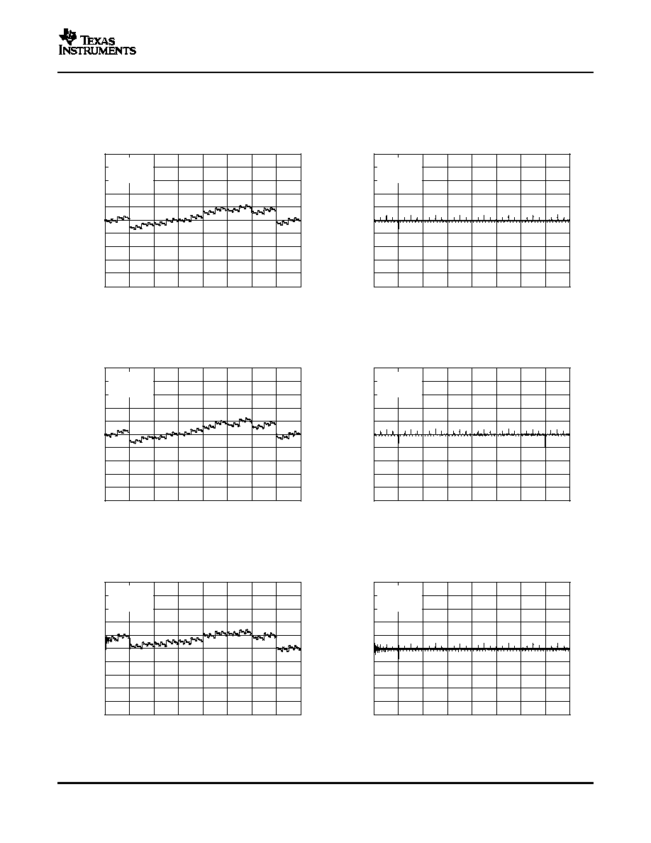
LINEARITY ERROR
DIFFERENTIAL LINEARITY ERROR
vs DIGITAL INPUT CODE
vs DIGITAL INPUT CODE
Figure 1.
Figure 2.
LINEARITY ERROR
DIFFERENTIAL LINEARITY ERROR
vs DIGITAL INPUT CODE
vs DIGITAL INPUT CODE
Figure 3.
Figure 4.
LINEARITY ERROR
DIFFERENTIAL LINEARITY ERROR
vs DIGITAL INPUT CODE
vs DIGITAL INPUT CODE
Figure 5.
Figure 6.
5
www.ti.com
PRODUCT PREVIEW
1.6
1.4
1.2
1.0
0.8
0.6
0.4
0.2
0
0
0.5
1.0
1.5
2.0
2.5
3.0
3.5
4.0
4.5
5.0
S
u
p
p
l
y
C
u
r
r
e
n
t
(
m
A
)
Logic Input Voltage (V)
V
DD
= +5.0V
V
DD
= +3.0V
6
0
-
6
-
12
-
18
-
24
-
30
-
36
-
42
-
48
-
54
-
60
-
66
-
72
-
78
-
84
-
90
-
96
-
102
10
100
1k
10k
100k
1M
10M
100M
A
t
t
e
n
u
a
t
i
o
n
(
d
B
)
Bandwidth (Hz)
Time (50ns/div)
O
u
t
p
u
t
V
o
l
t
a
g
e
(
5
0
m
V
/
d
i
v
)
Code 2047 to 2048
DAC Update
Bipolar Configuration:
±
10V
OUT
Time (50ns/div)
O
u
t
p
u
t
V
o
l
t
a
g
e
(
5
0
m
V
/
d
i
v
)
Code 2048 to 2047
DAC Update
Bipolar Configuration:
±
10V
OUT
Time (20ns/div)
O
u
t
p
u
t
V
o
l
t
a
g
e
(
2
0
m
V
/
d
i
v
)
Small Signal Settling
DAC Update
0
-
0.2
-
0.4
-
0.6
-
0.8
-
1.0
-
1.2
-
1.4
-
1.6
-
1.8
-
2.0
-
40
-
20
0
20
40
60
80
100
120
G
a
i
n
E
r
r
o
r
(
m
V
)
Temperature (
_
C)
V
REF
= +10V
DAC7811
SBAS337 ≠ APRIL 2005
TYPICAL CHARACTERISTICS: V
DD
= +5 V (continued)
At T
A
= +25
∞
C, +V
DD
= +5 V, unless otherwise noted.
SUPPLY CURRENT
vs LOGIC INPUT VOLTAGE
REFERENCE MULTIPLYING BANDWIDTH
Figure 7.
Figure 8.
MIDSCALE DAC GLITCH
MIDSCALE DAC GLITCH
Figure 9.
Figure 10.
GAIN ERROR
DAC SETTLING TIME
vs TEMPERATURE
Figure 11.
Figure 12.
6
www.ti.com
PRODUCT PREVIEW
2.0
1.8
1.6
1.4
1.2
1.0
0.8
0.6
0.4
0.2
0
-
40
-
20
0
20
40
60
80
100
120
Q
u
i
e
s
c
e
n
t
C
u
r
r
e
n
t
(
µ
A
)
Temperature (
_
C)
V
REF
= +10V
V
DD
= +5.0V
V
DD
= +3.0V
1.6
1.4
1.2
1.0
0.8
0.6
0.4
0.2
0
-
40
-
20
0
20
40
60
80
100
120
O
u
t
p
u
t
L
e
a
k
a
g
e
(
n
A
)
Temperature (
_
C)
V
REF
= +10V
TYPICAL CHARACTERISTICS: V
DD
= +3 V
1.0
0.8
0.6
0.4
0.2
0
-
0.2
-
0.4
-
0.6
-
0.8
-
1.0
0
512
1024
1536
2048
2560
3072
3584
4096
I
N
L
(
L
S
B
)
Digital Input Code
T
A
= +25
_
C
V
REF
= +10V
1.0
0.8
0.6
0.4
0.2
0
-
0.2
-
0.4
-
0.6
-
0.8
-
1.0
0
512
1024
1536
2048
2560
3072
3584
4096
D
N
L
(
L
S
B
)
Digital Input Code
T
A
= +25
_
C
V
REF
= +10V
DAC7811
SBAS337 ≠ APRIL 2005
TYPICAL CHARACTERISTICS: V
DD
= +5 V (continued)
At T
A
= +25
∞
C, +V
DD
= +5 V, unless otherwise noted.
SUPPLY CURRENT
OUTPUT LEAKAGE
vs TEMPERATURE
vs TEMPERATURE
Figure 13.
Figure 14.
At T
A
= +25
∞
C, +V
DD
= +3 V, unless otherwise noted.
LINEARITY ERROR
DIFFERENTIAL LINEARITY ERROR
vs DIGITAL INPUT CODE
vs DIGITAL INPUT CODE
Figure 15.
Figure 16.
7
www.ti.com
PRODUCT PREVIEW
1.0
0.8
0.6
0.4
0.2
0
-
0.2
-
0.4
-
0.6
-
0.8
-
1.0
0
512
1024
1536
2048
2560
3072
3584
4096
I
N
L
(
L
S
B
)
Digital Input Code
T
A
=
-
40
_
C
V
REF
= +10V
1.0
0.8
0.6
0.4
0.2
0
-
0.2
-
0.4
-
0.6
-
0.8
-
1.0
0
512
1024
1536
2048
2560
3072
3584
4096
D
N
L
(
L
S
B
)
Digital Input Code
T
A
=
-
40
_
C
V
REF
= +10V
1.0
0.8
0.6
0.4
0.2
0
-
0.2
-
0.4
-
0.6
-
0.8
-
1.0
0
512
1024
1536
2048
2560
3072
3584
4096
I
N
L
(
L
S
B
)
Digital Input Code
T
A
= +125
_
C
V
REF
= +10V
1.0
0.8
0.6
0.4
0.2
0
-
0.2
-
0.4
-
0.6
-
0.8
-
1.0
0
512
1024
1536
2048
2560
3072
3584
4096
D
N
L
(
L
S
B
)
Digital Input Code
T
A
= +125
_
C
V
REF
= +10V
Time (50ns/div)
O
u
t
p
u
t
V
o
l
t
a
g
e
(
5
0
m
V
/
d
i
v
)
Code 2048 to 2047
DAC Update
Bipolar Configuration:
±
10V
OUT
Time (50ns/div)
O
u
t
p
u
t
V
o
l
t
a
g
e
(
5
0
m
V
/
d
i
v
)
Code 2047 to 2048
DAC Update
Bipolar Configuration:
±
10V
OUT
DAC7811
SBAS337 ≠ APRIL 2005
TYPICAL CHARACTERISTICS: V
DD
= +3 V (continued)
At T
A
= +25
∞
C, +V
DD
= +3 V, unless otherwise noted.
LINEARITY ERROR
DIFFERENTIAL LINEARITY ERROR
vs DIGITAL INPUT CODE
vs DIGITAL INPUT CODE
Figure 17.
Figure 18.
LINEARITY ERROR
DIFFERENTIAL LINEARITY ERROR
vs DIGITAL INPUT CODE
vs DIGITAL INPUT CODE
Figure 19.
Figure 20.
MIDSCALE DAC GLITCH
MIDSCALE DAC GLITCH
Figure 21.
Figure 22.
8
www.ti.com
PRODUCT PREVIEW
0
-
0.2
-
0.4
-
0.6
-
0.8
-
1.0
-
1.2
-
1.4
-
1.6
-
1.8
-
2.0
-
40
-
20
0
20
40
60
80
100
120
G
a
i
n
E
r
r
o
r
(
m
V
)
Temperature (
_
C)
V
REF
= +10V
1.6
1.4
1.2
1.0
0.8
0.6
0.4
0.2
0
-
40
-
20
0
20
40
60
80
100
120
O
u
t
p
u
t
L
e
a
k
a
g
e
(
n
A
)
Temperature (
_
C)
V
REF
= +10V
Theory of Operation
R
R
R
R
2R
2R
2R
2R
R
FB
I
OUT2
I
OUT 1
2R
V
REF
DB0
(LSB)
DB9
DB10
DB11
(MSB)
V
OUT
+ *
V
REF
CODE
4096
(1)
DAC7811
SBAS337 ≠ APRIL 2005
TYPICAL CHARACTERISTICS: V
DD
= +3 V (continued)
At T
A
= +25
∞
C, +V
DD
= +3 V, unless otherwise noted.
GAIN ERROR
OUTPUT LEAKAGE
vs TEMPERATURE
vs TEMPERATURE
Figure 23.
Figure 24.
The DAC7811 is a single channel current output, 12-bit digital-to-analog converter (DAC). The architecture,
illustrated in Figure 25, is an R-2R ladder configuration with the three MSBs segmented. Each 2R leg of the
ladder is either switched to I
OUT1
or the I
OUT2
terminal. The I
OUT1
terminal of the DAC is held at a virtual GND
potential by the use of an external I/V converter op amp. The R-2R ladder is connected to an external reference
input V
REF
that determines the DAC full-scale current. The R-2R ladder presents a code independent load
impedance to the external reference of 10 k
±
20%. The external reference voltage can vary in a range of ≠15 V
to +15 V, thus providing bipolar I
OUT
current operation. By using an external I/V converter and the DAC7811 R
FB
resistor, output voltage ranges of -V
REF
to V
REF
can be generated.
Figure 25. Equivalent R-2R DAC Circuit
When using an external I/V converter and the DAC7811 R
FB
resistor, the DAC output voltage is given by
Equation 1:
Each DAC code determines the 2R leg switch position to either GND or I
OUT
. Because the DAC output
impedance as seen looking into the I
OUT1
terminal changes versus code, the external I/V converter noise gain will
also change. Because of this, the external I/V converter op amp must have a sufficiently low offset voltage such
that the amplifier offset is not modulated by the DAC I
OUT1
terminal impedance change. External op amps with
large offset voltages can produce INL errors in the transfer function of the DAC7811 due to offset modulation
versus DAC code.
9
www.ti.com
PRODUCT PREVIEW
OPA277
DAC7811
I
OUT1
V
OUT
15V
V+
V
-
-
15V
R
FB
GND
V
DD
V
DD
V
REF
I
OUT2
Serial Interface
Input Shift Register
DAC7811
SBAS337 ≠ APRIL 2005
Theory of Operation (continued)
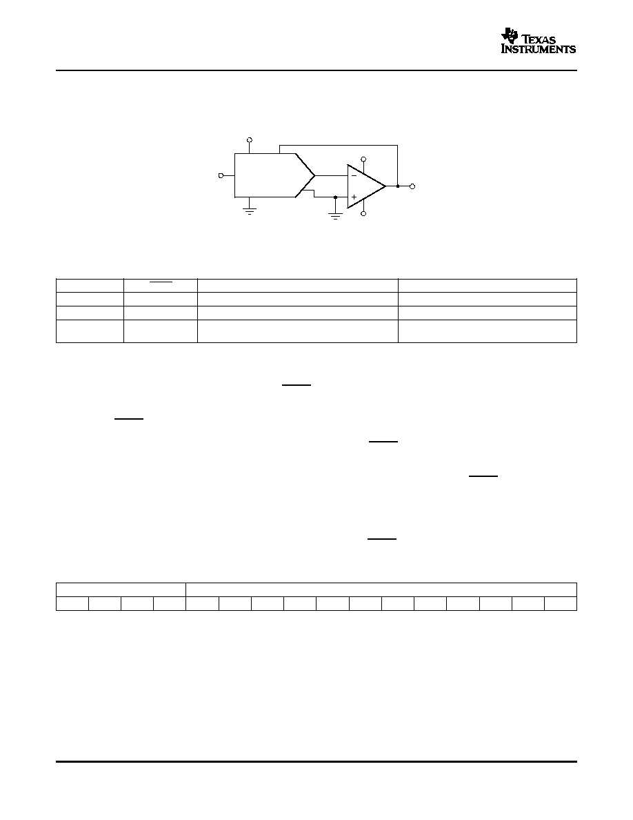
For best linearity performance of the DAC7811, an op amp (OPA277) is recommended (see Figure 26). This
circuit allows V
REF
swinging from ≠10 V to +10 V.
Figure 26. Voltage Output Configuration
Table 2. Control Logic Truth Table
(1)
CLK
SYNC
SERIAL SHIFT REGISTER
DAC REGISTER
X
H
No effect
Latched
+
L
Shift register data advanced one bit
Latched
X
+
In daisy-chain mode the function as determined by
In daisy-chain mode the contents may chage
C3-C0 is executed.
as determined by C3-C0.
(1)
+ Positive logic transition; X = Do not care.
The DAC7811 has a three-wire serial interface (SYNC, SCLK, and SDIN), which is compatible with SPI, QSPI,
and MICROWIRE interface standards as well as most Digital Signal Processor (DSP) devices. See the Serial
Write Operation timing diagram for an example of a typical write sequence. The write sequence begins by
bringing the SYNC line low. Data from the DIN line is clocked into the 16-bit shift register on the falling edge of
SCLK. The serial clock frequency can be as high as 50MHz, making the DAC7811 compatible with high-speed
DSPs. The SDIN and SCLK input buffers are gated off while SYNC is high which minimizes the power
dissipation of the digital interface. After SYNC goes low, the digital interface will respond to the SDIN and SCLK
input signals and data can now be shifted into the device. If an inactive clock edge occurs after SYNC goes low,
but before the first active clock edge, it will be ignored. If the SDO pin is being used then SYNC must remain low
until after the inactive clock edge that follows the 16th active clock edge.
The input shift register is 16 bits wide, as shown in Figure 27. The four MSBs are the control bits C3 ≠ C0; these
bits determine which function will be executed at the rising edge of SYNC in daisy-chain mode or the 16th active
clock edge in stand-alone mode. The remaining 12 bits are the data bits. On a load and update command
(C3≠C0 = 0001) these 12 data bits will be transferred to the DAC register; otherwise, they have no effect.
4 CONTROL BITS
12 DATA BITS
C3
C2
C1
C0
DB11
DB10
DB9
DB8
DB7
DB6
DB5
DB4
DB3
DB2
DB1
DB0
MSB
LSB
DB15
Figure 27. Contents of the 16-Bit Input Shift Register
10
www.ti.com
PRODUCT PREVIEW
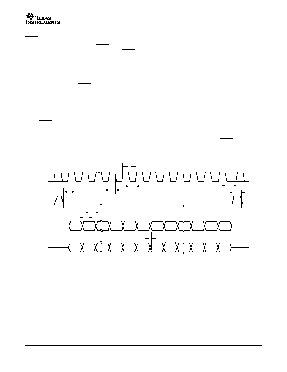
SYNC Interrupt
Daisy-Chain
t
CSS
t
CH
t
DS
t
DH
t
DDS
t
CC
t
CST
t
9
t
C
SCLK
SYNC
SDIN
DB15
(N)
DB0
(N)
DB15
(N)
DB0
(N)
DB15
(N + 1)
DB0
(N + 1)
SDO
Control Bits C3 to C0
DAC7811
SBAS337 ≠ APRIL 2005
In a normal write sequence, the SYNC line is kept low for at least 16 falling edges of SCLK and the DAC is
updated on the 16th falling edge. However, if SYNC is brought high before the 16th falling edge, this acts as an
interrupt to the write sequence. The shift register is reset and the write sequence is seen as invalid. Neither an
update of the DAC register contents or a change in the operating mode occurs.
The DAC7811 powers up in the daisy chain mode which must be used when 2 or more devices are connected in
tandem. The SCLK and SYNC signals are shared across all devices while the SDO output of the first device
connects to the SDIN input of the following device, and so forth. In this configuration 16 SCLK cycles for each
DAC7811 in the chain are required. Please refer to the timing diagram of Figure 28.
For n devices in a daisy-chain configuration, 16n SCLK cycles are required to shift in the entire input data
stream. After 16n active SCLK edges are received following a falling SYNC, the data stream becomes complete,
and SYNC can brought high to update n devices simultaneously.
When SYNC is brought high, each device will execute the function defined by the four DAC control bits C3-C0 in
its input shift register. For example, C3-C0 must be 0001 for each DAC in the chain that is to be updated with
new data, and C3-C0 must be 0000 for each DAC in the chain whose contents are to remain unchanged.
A continuous stream containing the exact number of SCLK cycles may be sent first while the SYNC signal is held
low, and then raise SYNC at a later time. Nothing happens until the rising edge of SYNC, and then each
DAC7811 in the chain will execute the function defined by the four DAC control bits C3-C0 in its input shift
register.
Figure 28. DAC7811 Timing Diagram
Control Bits C3 to C0 allow control of various functions of the DAC; see Table 3. Default settings of the DAC on
powering up are as follows: Data clocked into shift register on falling clock edges; daisy-chain mode is enabled.
Device powers on with zero-scale loaded into the DAC register and IOUT lines. The DAC control bits allow the
user to adjust certain features as part of an initialization sequence, for example, daisy-chaining may be disabled
if not in use, active clock edge may be changed to rising edge, and DAC output may be cleared to either zero or
midscale. The user may also initiate a readback of the DAC register contents for verification purposes.
11
www.ti.com
PRODUCT PREVIEW
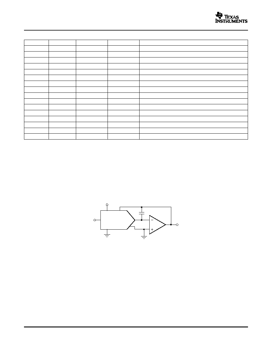
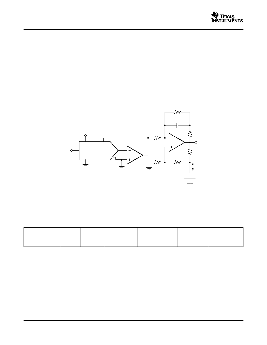
APPLICATION INFORMATION
Stability Circuit
I
OUT1
V
OUT
R
FB
C
1
GND
V
DD
V
DD
U1
U2
V
REF
V
REF
I
OUT2
Positive Voltage Output Circuit
DAC7811
SBAS337 ≠ APRIL 2005
Table 3. Serial Input Register Data Format, Data Loaded MSB First
C3
C2
C1
C0
FUNCTION IMPLEMENTED
0
0
0
0
No operation (power-on default)
0
0
0
1
Load and update
0
0
1
0
Initiate readback
0
0
1
1
Reserved
0
1
0
0
Reserved
0
1
0
1
Reserved
0
1
1
0
Reserved
0
1
1
1
Reserved
1
0
0
0
Reserved
1
0
0
1
Daisy-chain disable
1
0
1
0
Clock data to shift register on rising edge
1
0
1
1
Clear DAC output to 0
1
1
0
0
Clear DAC output to midscale
1
1
0
1
Reserved
1
1
1
0
Reserved
1
1
1
1
Reserved
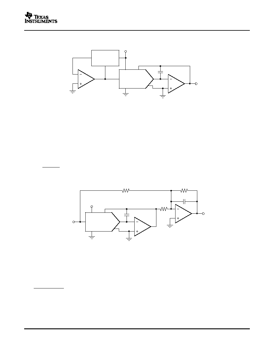
For a current-to-voltage design (see Figure 29), the DAC7811 current output (I
OUT
) and the connection with the
inverting node of the op amp should be as short as possible and according to correct printed circuit board (PCB)
layout design. For each code change, there is a step function. If the gain bandwidth product (GBP) of the op amp
is limited and parasitic capacitance is excessive at the inverting node, then gain peaking is possible. Therefore,
for circuit stability, a compensation capacitor C1 (4 pF to 20 pF typ) can be added to the design, as shown in
Figure 29.
Figure 29. Gain Peaking Prevention Circuit with Compensation Capacitor
As Figure 30 illustrates, in order to generate a positive voltage output, a negative reference is input to the
DAC7811. This design is suggested instead of using an inverting amp to invert the output as a result of resistor
tolerance errors. For a negative reference, V
OUT
and GND of the reference are level-shifted to a virtual ground
and a ≠2.5 V input to the DAC7811 with an op amp.
12
www.ti.com
PRODUCT PREVIEW
V
OUT
R
FB
C
1
I
OUT1
0
V
OUT
+2.5V
GND
GND
-
2.5V
V
OUT
V
IN
V
REF
+2.5V Reference
V
DD
V
DD
DAC7811
OPA277
OPA277
I
OUT2
Bipolar Output Section
V
OUT
+
D
0.5
2
N
*
1
V
REF
(2)
I
OUT1
R
FB
C
1
GND
V
DD
V
DD
+2.5V
(+10V)
V
REF
V
OUT
C
2
U4
OPA277
10k
10k
5k
-
2.5V
V
OUT
+2.5V
(
-
10V
V
OUT
+10V)
U2
OPA277
DAC7811
I
OUT2
Programmable Current Source Circuit
I
L
+
(
R2
)
R3
)
R1
R3
V
REF
D
(3)
DAC7811
SBAS337 ≠ APRIL 2005
APPLICATION INFORMATION (continued)
Figure 30. Positive Voltage Output Circuit
The DAC7811, as a 2-quadrant multiplying DAC, can be used to generate a unipolar output. The polarity of the
full-scale output I
OUT
is the inverse of the input reference voltage at V
REF
.
Some applications require full 4-quadrant multiplying capabilities or bipolar output swing. As shown in Figure 31,
external op amp U4 is added as a summing amp and has a gain of 2X that widens the output span to 5 V. A
4-quadrant multiplying circuit is implemented by using a 2.5 V offset of the reference voltage to bias U4.
According to the circuit transfer equation given in Equation 2, input data (D) from code 0 to full-scale produces
output voltages of V
OUT
= ≠2.5 V to V
OUT
= +2.5 V.
External resistance mismatching is the significant error in Figure 31.
Figure 31. Bipolar Output Circuit
A DAC7811 can be integrated into the circuit in Figure 32 to implement an improved Howland current pump for
precise voltage to current conversions. Bidirectional current flow and high voltage compliance are two features of
the circuit. With a matched resistor network, the load current of the circuit is shown by Equation 3:
13
www.ti.com
PRODUCT PREVIEW
Z
O
+
R1 R3
(
R1
)
R2
)
R1
(
R2
)
R3
) *
R1
(
R2
)
R3
)
(4)
R2
15k
I
OUT1
R
FB
GND
V
DD
V
DD
V
REF
V
OUT
I
L
LOAD
C
1
10pF
U2
OPA277
R1
150k
R3
50k
R3
50
R1
150k
R2
15k
U2
OPA277
U1
DAC7811
I
OUT2
Cross-Reference
DAC7811
SBAS337 ≠ APRIL 2005
APPLICATION INFORMATION (continued)
The value of R3 in the previous equation can be reduced to increase the output current drive of U3. U3 can drive
±
20 mA in both directions with voltage compliance limited up to 15 V by the U3 voltage supply. Elimination of the
circuit compensation capacitor C1 in the circuit is not suggested as a result of the change in the output
impedance Z
O
, according to Equation 4:
As shown in Equation 4, with matched resistors, Z
O
is infinite and the circuit is optimum for use as a current
source. However, if unmatched resistors are used, Z
O
is positive or negative with negative output impedance
being a potential cause of oscillation. Therefore, by incorporating C1 into the circuit, possible oscillation problems
are eliminated. The value of C1 can be determined for critical applications; for most applications, however, a
value of several pF is suggested.
Figure 32. Programmable Bidirectional Current Source Circuit
The DAC7811 has an industry-standard pinout. Table 4 provides the cross-reference information.
Table 4. Cross-Reference
SPECIFIED
TEMPERATURE
PACKAGE
PACKAGE
CROSS-
PRODUCT
INL (LSB)
DNL (LSB)
RANGE
DESCRIPTION
OPTION
REFERENCE PART
DAC7811
±
1
±
1
≠40
∞
C to +125
∞
C
10-Lead MicroSOIC
MSOP-10
AD5443YRM
14
PACKAGING INFORMATION
Orderable Device
Status
(1)
Package
Type
Package
Drawing
Pins Package
Qty
Eco Plan
(2)
Lead/Ball Finish
MSL Peak Temp
(3)
DAC7811IDGSR
PREVIEW
MSOP
DGS
10
2500
TBD
Call TI
Call TI
DAC7811IDGST
PREVIEW
MSOP
DGS
10
250
TBD
Call TI
Call TI
DAC7811IDRCR
PREVIEW
SON
DRC
10
3000
TBD
Call TI
Call TI
DAC7811IDRCT
PREVIEW
SON
DRC
10
250
TBD
Call TI
Call TI
(1)
The marketing status values are defined as follows:
ACTIVE: Product device recommended for new designs.
LIFEBUY: TI has announced that the device will be discontinued, and a lifetime-buy period is in effect.
NRND: Not recommended for new designs. Device is in production to support existing customers, but TI does not recommend using this part in
a new design.
PREVIEW: Device has been announced but is not in production. Samples may or may not be available.
OBSOLETE: TI has discontinued the production of the device.
(2)
Eco
Plan
-
The
planned
eco-friendly
classification:
Pb-Free
(RoHS)
or
Green
(RoHS
&
no
Sb/Br)
-
please
check
http://www.ti.com/productcontent
for the latest availability information and additional product content details.
TBD: The Pb-Free/Green conversion plan has not been defined.
Pb-Free (RoHS): TI's terms "Lead-Free" or "Pb-Free" mean semiconductor products that are compatible with the current RoHS requirements
for all 6 substances, including the requirement that lead not exceed 0.1% by weight in homogeneous materials. Where designed to be soldered
at high temperatures, TI Pb-Free products are suitable for use in specified lead-free processes.
Green (RoHS & no Sb/Br): TI defines "Green" to mean Pb-Free (RoHS compatible), and free of Bromine (Br) and Antimony (Sb) based flame
retardants (Br or Sb do not exceed 0.1% by weight in homogeneous material)
(3)
MSL, Peak Temp. -- The Moisture Sensitivity Level rating according to the JEDEC industry standard classifications, and peak solder
temperature.
Important Information and Disclaimer:The information provided on this page represents TI's knowledge and belief as of the date that it is
provided. TI bases its knowledge and belief on information provided by third parties, and makes no representation or warranty as to the
accuracy of such information. Efforts are underway to better integrate information from third parties. TI has taken and continues to take
reasonable steps to provide representative and accurate information but may not have conducted destructive testing or chemical analysis on
incoming materials and chemicals. TI and TI suppliers consider certain information to be proprietary, and thus CAS numbers and other limited
information may not be available for release.
In no event shall TI's liability arising out of such information exceed the total purchase price of the TI part(s) at issue in this document sold by TI
to Customer on an annual basis.
PACKAGE OPTION ADDENDUM
www.ti.com
6-Apr-2005
Addendum-Page 1


IMPORTANT NOTICE
Texas Instruments Incorporated and its subsidiaries (TI) reserve the right to make corrections, modifications,
enhancements, improvements, and other changes to its products and services at any time and to discontinue
any product or service without notice. Customers should obtain the latest relevant information before placing
orders and should verify that such information is current and complete. All products are sold subject to TI's terms
and conditions of sale supplied at the time of order acknowledgment.
TI warrants performance of its hardware products to the specifications applicable at the time of sale in
accordance with TI's standard warranty. Testing and other quality control techniques are used to the extent TI
deems necessary to support this warranty. Except where mandated by government requirements, testing of all
parameters of each product is not necessarily performed.
TI assumes no liability for applications assistance or customer product design. Customers are responsible for
their products and applications using TI components. To minimize the risks associated with customer products
and applications, customers should provide adequate design and operating safeguards.
TI does not warrant or represent that any license, either express or implied, is granted under any TI patent right,
copyright, mask work right, or other TI intellectual property right relating to any combination, machine, or process
in which TI products or services are used. Information published by TI regarding third-party products or services
does not constitute a license from TI to use such products or services or a warranty or endorsement thereof.
Use of such information may require a license from a third party under the patents or other intellectual property
of the third party, or a license from TI under the patents or other intellectual property of TI.
Reproduction of information in TI data books or data sheets is permissible only if reproduction is without
alteration and is accompanied by all associated warranties, conditions, limitations, and notices. Reproduction
of this information with alteration is an unfair and deceptive business practice. TI is not responsible or liable for
such altered documentation.
Resale of TI products or services with statements different from or beyond the parameters stated by TI for that
product or service voids all express and any implied warranties for the associated TI product or service and
is an unfair and deceptive business practice. TI is not responsible or liable for any such statements.
Following are URLs where you can obtain information on other Texas Instruments products and application
solutions:
Products
Applications
Amplifiers
amplifier.ti.com
Audio
www.ti.com/audio
Data Converters
dataconverter.ti.com
Automotive
www.ti.com/automotive
DSP
dsp.ti.com
Broadband
www.ti.com/broadband
Interface
interface.ti.com
Digital Control
www.ti.com/digitalcontrol
Logic
logic.ti.com
Military
www.ti.com/military
Power Mgmt
power.ti.com
Optical Networking
www.ti.com/opticalnetwork
Microcontrollers
microcontroller.ti.com
Security
www.ti.com/security
Telephony
www.ti.com/telephony
Video & Imaging
www.ti.com/video
Wireless
www.ti.com/wireless
Mailing Address:
Texas Instruments
Post Office Box 655303 Dallas, Texas 75265
Copyright
2005, Texas Instruments Incorporated