
Burr Brown Products
from Texas Instruments
DAC7822
FEATURES
DESCRIPTION
APPLICATIONS
12-Bit
R-2R DAC A
12-Bit
R-2R DAC B
LATCH
R A
FB
I
1A
OUT
I
2A
OUT
I
1B
OUT
DAC /B
A
CS
R/W
V
DD
DB0
DATA
INPUTS
DB11
LDAC
CLR
I
2B
OUT
LATCH
INPUT
BUFFER
CONTROL
LOGIC
R
1
2R
R
FB
2R
R
3
2R
R A
3
R
A
2_3
R A
2
V
A
REF
R A
1
R
2
2R
R
3
2R
R
2
2R
GND
POWER-ON
RESET
R B
3
R
B
2_3
R B
2
V
B
REF
R B
1
R
FB
B
R
1
2R
R
FB
2R
DAC7822
SBAS374 ≠ JUNE 2006
Dual, 12-Bit, Parallel Input, Multiplying
Digital-to-Analog Converter
∑
±
1LSB INL
The DAC7822 is a dual, CMOS, 12-bit, current
output digital-to-analog converter (DAC). This device
∑
2.5V to 5.5V Supply Operation
operates from a 2.5V to 5.5V power supply, making it
∑
Fast Parallel Interface:
suitable
for
battery-powered
and
many
other
17ns Write Cycle
applications.
∑
Update Rate of 20.4MSPS
The DAC7822 operates with a fast parallel interface.
∑
10MHz Multiplying Bandwidth
Data readback allows the user to read the contents
∑
±
15V Reference Input
of the DAC register via the DB pins. On power-up,
the internal register and latches are filled with zeroes
∑
Extended Temperature Range:
and the DAC outputs are at zero scale.
≠40
∞
C to +125
∞
C
The
DAC7822
offers
excellent
4-quadrant
∑
40-Lead QFN
multiplication
characteristics,
with
large
signal
∑
12-Bit Monotonic
multiplying
bandwidth
of
10MHz.
The
applied
∑
4-Quadrant Multiplication
external reference input voltage (V
REF
) determines
∑
Power-On Reset with Brownout Detection
the full-scale output current. An integrated feedback
resistor (R
FB
) provides temperature tracking and
∑
Readback Function
full-scale voltage output when combined with an
∑
Industry-Standard Pin Configuration
external current-to-voltage precision amplifier. The
∑
Pin-Compatible with the AD5405
DAC7822 also includes the resistors necessary for
4-quadrant multiplication and other configuration
modes.
∑
Portable Battery-Powered Instruments
The DAC7822 is available in a 40-lead QFN
∑
Waveform Generators
package.
∑
Analog Processing
∑
Programmable Amplifiers and Attenuators
∑
Digitally-Controlled Calibration
∑
Programmable Filters and Oscillators
∑
Ultrasound
Please be aware that an important notice concerning availability, standard warranty, and use in critical applications of Texas
Instruments semiconductor products and disclaimers thereto appears at the end of this data sheet.
All trademarks are the property of their respective owners.
PRODUCTION DATA information is current as of publication date.
Copyright © 2006, Texas Instruments Incorporated
Products conform to specifications per the terms of the Texas
Instruments standard warranty. Production processing does not
necessarily include testing of all parameters.
www.ti.com
ABSOLUTE MAXIMUM RATINGS
DAC7822
SBAS374 ≠ JUNE 2006
This integrated circuit can be damaged by ESD. Texas Instruments recommends that all integrated circuits be handled with
appropriate precautions. Failure to observe proper handling and installation procedures can cause damage.
ESD damage can range from subtle performance degradation to complete device failure. Precision integrated circuits may be
more susceptible to damage because very small parametric changes could cause the device not to meet its published
specifications.
ORDERING INFORMATION
(1)
SPECIFIED
PACKAGE
TEMPERATURE
PACKAGE
ORDERING
TRANSPORT MEDIA,
PRODUCT
PACKAGE
DESIGNATOR
RANGE
MARKING
NUMBER
QUANTITY
DAC7822IRTAT
250, Tape and Reel
DAC7822
40-QFN
RTA
≠40
∞
C to +125
∞
C
DAC7822
DAC7822IRTAR
2000, Tape and Reel
(1)
For the most current specifications and package information, see the Package Option Addendum at the end of this data sheet, or refer
to our web site at
www.ti.com
.
over operating free-air temperature range (unless otherwise noted)
(1)
DAC7822
UNIT
V
DD
to GND
≠0.3 to +7.0
V
Digital input voltage to GND
≠0.3 to V
DD
+ 0.3
V
V
OUT
to GND
≠0.3 to V
DD
+ 0.3
V
Operating temperature range
≠40 to +125
∞
C
Storage temperature range
≠65 to +150
∞
C
Junction temperature (T
J
max)
+150
∞
C
ESD Rating, HBM
2000
V
ESD Rating, CDM
1000
V
(1)
Stresses above those listed under absolute maximum ratings may cause permanent damage to the device. Exposure to absolute
maximum conditions for extended periods may affect device reliability.
2
Submit Documentation Feedback
www.ti.com
ELECTRICAL CHARACTERISTICS
DAC7822
SBAS374 ≠ JUNE 2006
V
DD
= +2.5V to +5.5V; I
OUT
1 = Virtual GND; I
OUT
2 = 0V; V
REF
= 10V; T
A
= full operating temperature. All specifications ≠40
∞
C
to +125
∞
C, unless otherwise noted.
DAC7822
PARAMETER
CONDITIONS
MIN
TYP
MAX
UNITS
STATIC PERFORMANCE
Resolution
12
Bits
Relative accuracy
±
1
LSB
Differential nonlinearity
±
1
LSB
Output leakage current
Data = 000h, T
A
= +25
∞
C
±
1
nA
Output leakage current
Data = 000h, T
A
= T
MAX
±
15
nA
Full-scale gain error
All ones loaded to DAC register
±
10
±
25
mV
Full-scale tempco
(1)
±
5
ppm/
∞
C
Bipolar zero-code error
Circuit configuration as shown in
Figure 41
±
25
mV
Output capacitance
DAC latches leaded with all 1s
25
30
pF
REFERENCE INPUT
V
REF
range
≠15
15
V
V
REF
A, V
REF
B, Input resistance
8
10
12
k
R
1
, R
FB
resistance
17
20
25
k
R
2
, R
3
resistance
17
20
25
k
V
REF
A to V
REF
B Input Mismatch
1.6
2.5
%
R
2
to R
3
Mismatch
0.06
0.18
%
LOGIC INPUTS AND OUTPUT
(1)
V
DD
= +2.5V
0.6
V
Input low voltage
V
IL
V
DD
= +5V
0.8
V
V
DD
= +2.5V
2.1
V
Input high voltage
V
IH
V
DD
= +5V
2.4
V
Input leakage current
I
IL
1
µA
Input capacitance
C
IL
10
pF
POWER REQUIREMENTS
V
DD
2.5
5.5
V
I
DD
(normal operation)
Logic inputs = 0V
5
µA
V
DD
= +4.5V to +5.5V
V
IH
= V
DD
and V
IL
= GND
0.8
5
µA
V
DD
= +2.5V to +3.6V
V
IH
= V
DD
and V
IL
= GND
0.4
2.5
µA
AC CHARACTERISTICS
(1)
Output voltage settling time
0.2
µs
Reference multiplying BW
V
REF
= 7V
PP
, Data = FFFh
10
MHz
V
REF
= 0V to 10V,
DAC glitch impulse
10
nV-s
Data = 7FFh to 800h to 7FFh
Feedthrough error V
OUT
/V
REF
Data = 000h, V
REF
= 100kHz
≠70
dB
Digital feedthrough
2
nV-s
Total harmonic distortion
≠105
dB
Output spot noise voltage
25
nV/
Hz
(1)
Specified by design and characterization; not production tested.
3
Submit Documentation Feedback
www.ti.com
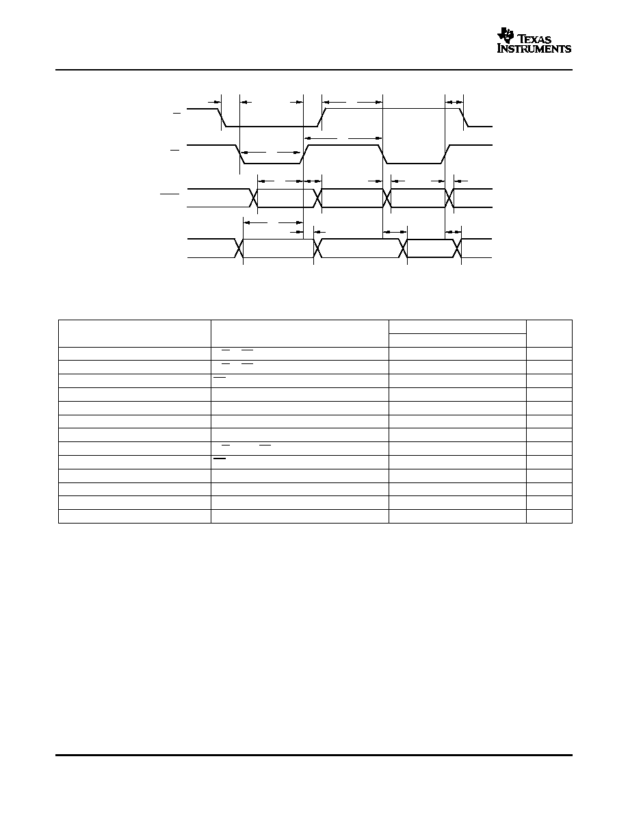
t
1
R/W
t
2
t
8
CS
DACA/DACB
t
3
t
t
4
t
6
t
7
t
13
t
12
t
10
t
11
t
5
t
2
DATA
9
DATA VALID
DATA VALID
TIMING REQUIREMENTS: 2.5 V to 5.5 V
DAC7822
SBAS374 ≠ JUNE 2006
TIMING INFORMATION
At t
r
= t
f
= 1ns (10% to 90% of V
DD
) and timed from a voltage level of (V
IL
+ V
IH
)/2; V
DD
= 2.5V to 5.5V, V
REF
= 10V,
I
OUT
2 = 0V. All specifications ≠40
∞
C to +125
∞
C, unless otherwise noted.
DAC7822
PARAMETER
(1)
TEST CONDITIONS
MIN
TYP
MAX
UNIT
t
1
R/W to CS setup time
0
ns
t
2
R/W to CS hold time
0
ns
t
3
CS low time (write cycle)
10
ns
t
4
Address setup time
10
ns
t
5
Address hold time
0
ns
t
6
Data setup time
6
ns
t
7
Data hold time
0
ns
t
8
R/W high to CS low
5
ns
t
9
CS minimum high time
7
ns
t
10
Address setup time (Read Cycle)
0
ns
t
11
Address hold time (Read Cycle)
0
ns
t
12
Data access time
5
35
ns
t
13
Bus relinquish time
5
10
ns
(1)
Ensured by design; not production tested.
4
Submit Documentation Feedback
www.ti.com
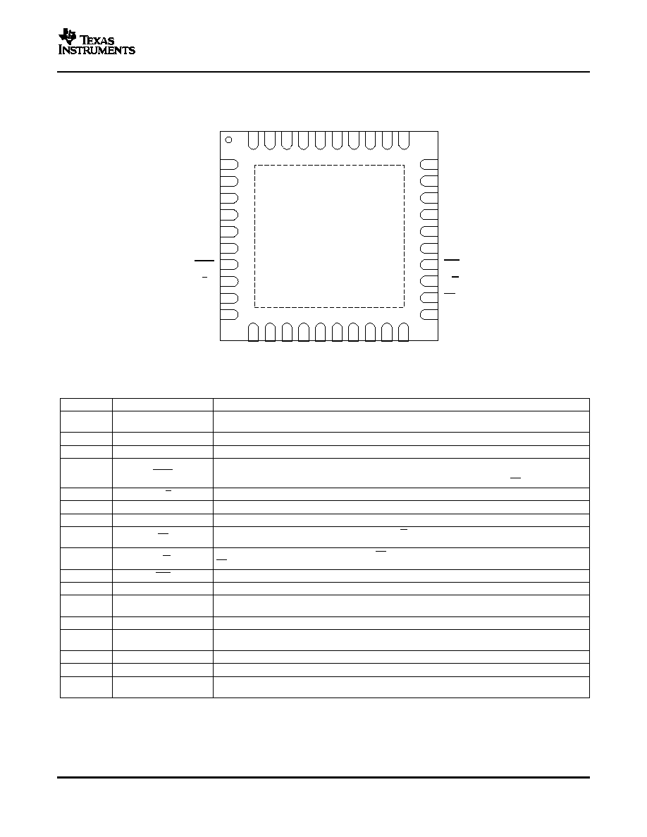
DEVICE INFORMATION
R A
1
R A
2
R
A
2_3
R A
3
V
A
REF
DGND
LDAC
DAC A/B
NC
DB11
R B
1
R B
2
R
B
2_3
R B
3
V
B
REF
V
DD
CLR
R/W
CS
DB0
1
2
3
4
5
6
7
8
9
10
30
29
28
27
26
25
24
23
22
21
DAC7822
11
12
13
14
15
16
17
18
19
20
DB10
DB9
DB8
DB7
DB6
DB5
DB4
DB3
DB2
DB1
40
39
38
37
36
35
34
33
32
31
R
A
F
B
I
2A
O
U
T
I
1A
O
U
T
NC
NC
NC
NC
I
1B
O
U
T
I
2B
O
U
T
R
B
F
B
DAC7822
SBAS374 ≠ JUNE 2006
TERMINAL FUNCTIONS
PIN NO.
PIN NAME
DESCRIPTION
DAC A 4-Quadrant Resistors. Allows a number of configuration modes, including bipolar operation with
1-4
R
1
A, R
2
A, R
2_3
A, R
3
A
minimum of external components.
5, 26
V
REF
A, V
REF
B
DAC Reference Voltage Input Terminals.
6
DGND
Digital Ground Pin.
Load DAC Input. Allows asynchronous or synchronous updates to the DAC output. The DAC is asynchronously
7
LDAC
updated when this signal goes low. Alternatively, if this line is held permanently low, an automatic or
synchronous update mode is selected whereby the DAC is updated on the rising edge of CS.
8
DAC A/B
Selects DAC A or B. Low selects DAC A, and high selects DAC B.
9, 34-37
NC
Not internally connected.
10-21
DB11 to DB0
Parallel Data Bits 11 through 0.
Chip Select Input; active low. Used in conjuction with R/W to load parallel data to the input latch or to read data
22
CS
from the DAC register. Edge sensitive; when pulled high, the DAC data is latched.
Read/Write. When low, used in conjunction with CS to load parallel data. When high, used in conjunction with
23
R/W
CS to read back contents of DAC register.
24
CLR
Active Low Control Input. Clears DAC output and input and DAC registers.
25
V
DD
Positive Power Supply Input. These parts can be operated from a supply of 2.5V to 5.5V.
DAC B 4-Quadrant Resistors. Allow a number of configuration modes, including bipolar operation with a
27-30
R
3
B, R
2_3
B, R
2
B, R
1
B
minimum of external components.
31, 40
R
FB
B, R
FB
A
External Amplifier Output.
DAC A Analog Ground. This pin typically should be tied to the analog ground of the system, but can be biased
32
I
OUT
2B
to achieve single-supply operation.
33
I
OUT
1B
DAC B Current Output.
38
I
OUT
1A
DAC A Current Output.
DAC A Analog Ground. This pin typically should be tied to the analog ground of the system, but can be biased
39
I
OUT
2A
to achieve single-supply operation.
5
Submit Documentation Feedback
www.ti.com
TYPICAL CHARACTERISTICS: V
DD
= +5V
Channel A
1.0
0.8
0.6
0.4
0.2
0
-0.2
-0.4
-0.6
-0.8
-1.0
0
512
1024
1536
2048
2560
3072
3584
4096
INL(LSB)
Digital Input Code
T
A
= +25∞C
V
= +10V
REF
1.0
0.8
0.6
0.4
0.2
0
-0.2
-0.4
-0.6
-0.8
-1.0
0
512
1024
1536
2048
2560
3072
3584
4096
DNL(LSB)
Digital Input Code
T
A
= +25∞C
V
= +10V
REF
1.0
0.8
0.6
0.4
0.2
0
-0.2
-0.4
-0.6
-0.8
-1.0
0
512
1024
1536
2048
2560
3072
3584
4096
INL(LSB)
Digital Input Code
T = 40
-
∞
A
C
V
= +10V
REF
1.0
0.8
0.6
0.4
0.2
0
-0.2
-0.4
-0.6
-0.8
-1.0
0
512
1024
1536
2048
2560
3072
3584
4096
DNL(LSB)
Digital Input Code
T
A
= -40∞C
V
= +10V
REF
1.0
0.8
0.6
0.4
0.2
0
-0.2
-0.4
-0.6
-0.8
-1.0
0
512
1024
1536
2048
2560
3072
3584
4096
INL(LSB)
Digital Input Code
T
A
= +125∞C
V
= +10V
REF
1.0
0.8
0.6
0.4
0.2
0
-0.2
-0.4
-0.6
-0.8
-1.0
0
512
1024
1536
2048
2560
3072
3584
4096
DNL(LSB)
Digital Input Code
T
A
= +125∞C
V
= +10V
REF
DAC7822
SBAS374 ≠ JUNE 2006
At T
A
= +25
∞
C, +V
DD
= +5V, unless otherwise noted.
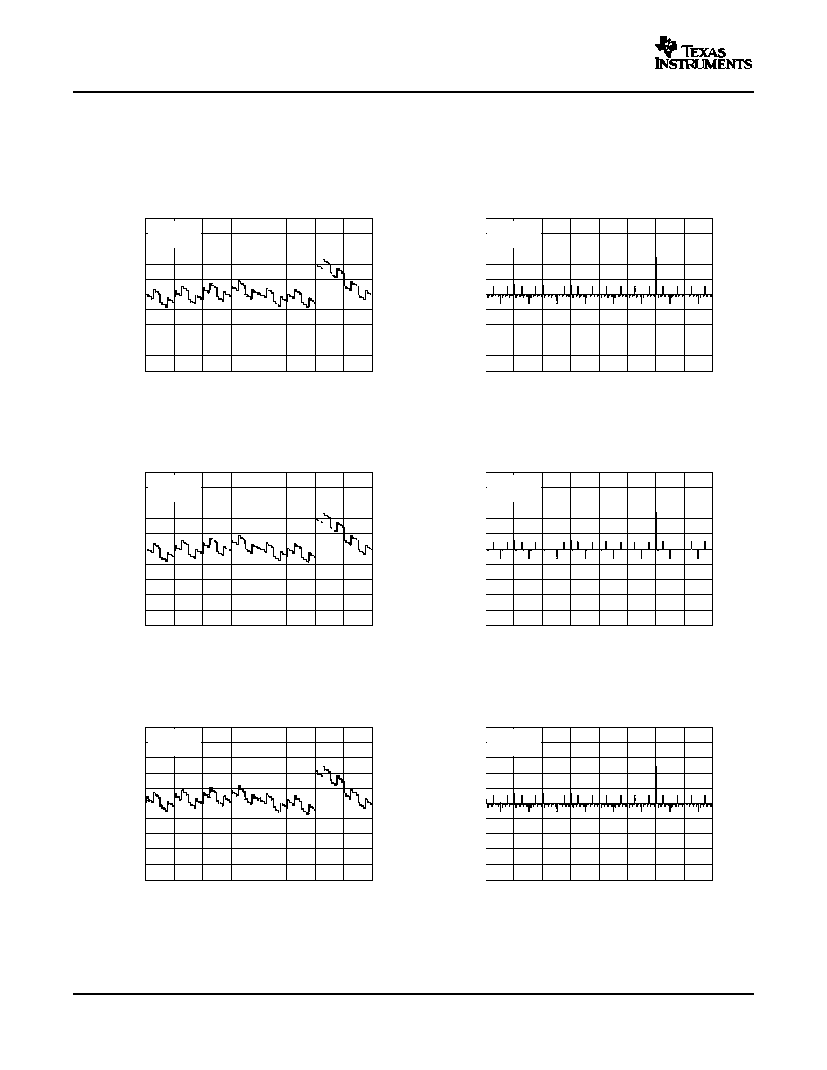
LINEARITY ERROR
DIFFERENTIAL LINEARITY ERROR
vs DIGITAL INPUT CODE
vs DIGITAL INPUT CODE
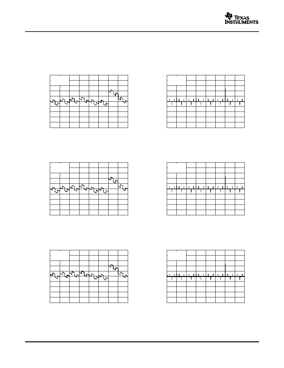
Figure 1.
Figure 2.
LINEARITY ERROR
DIFFERENTIAL LINEARITY ERROR
vs DIGITAL INPUT CODE
vs DIGITAL INPUT CODE
Figure 3.
Figure 4.
LINEARITY ERROR
DIFFERENTIAL LINEARITY ERROR
vs DIGITAL INPUT CODE
vs DIGITAL INPUT CODE
Figure 5.
Figure 6.
6
Submit Documentation Feedback
www.ti.com
Channel B
1.0
0.8
0.6
0.4
0.2
0
-0.2
-0.4
-0.6
-0.8
-1.0
0
512
1024
1536
2048
2560
3072
3584
4096
INL(LSB)
Digital Input Code
T
A
= +25∞C
V
= +10V
REF
1.0
0.8
0.6
0.4
0.2
0
-0.2
-0.4
-0.6
-0.8
-1.0
0
512
1024
1536
2048
2560
3072
3584
4096
DNL(LSB)
Digital Input Code
T
A
= +25∞C
V
= +10V
REF
1.0
0.8
0.6
0.4
0.2
0
-0.2
-0.4
-0.6
-0.8
-1.0
0
512
1024
1536
2048
2560
3072
3584
4096
INL(LSB)
Digital Input Code
T
40∞
A
= -
C
V
= +10V
REF
1.0
0.8
0.6
0.4
0.2
0
-0.2
-0.4
-0.6
-0.8
-1.0
0
512
1024
1536
2048
2560
3072
3584
4096
DNL(LSB)
Digital Input Code
T
-
∞
A
= 40 C
V
= +10V
REF
1.0
0.8
0.6
0.4
0.2
0
-0.2
-0.4
-0.6
-0.8
-1.0
0
512
1024
1536
2048
2560
3072
3584
4096
INL(LSB)
Digital Input Code
T
A
= +125∞C
V
= +10V
REF
1.0
0.8
0.6
0.4
0.2
0
-0.2
-0.4
-0.6
-0.8
-1.0
0
512
1024
1536
2048
2560
3072
3584
4096
DNL(LSB)
Digital Input Code
T
A
= +125∞C
V
= +10V
REF
DAC7822
SBAS374 ≠ JUNE 2006
TYPICAL CHARACTERISTICS: V
DD
= +5V (continued)
At T
A
= +25
∞
C, +V
DD
= +5V, unless otherwise noted.
LINEARITY ERROR
DIFFERENTIAL LINEARITY ERROR
vs DIGITAL INPUT CODE
vs DIGITAL INPUT CODE
Figure 7.
Figure 8.
LINEARITY ERROR
DIFFERENTIAL LINEARITY ERROR
vs DIGITAL INPUT CODE
vs DIGITAL INPUT CODE
Figure 9.
Figure 10.
LINEARITY ERROR
DIFFERENTIAL LINEARITY ERROR
vs DIGITAL INPUT CODE
vs DIGITAL INPUT CODE
Figure 11.
Figure 12.
7
Submit Documentation Feedback
www.ti.com
6
0
6
12
18
24
30
36
42
48
56
60
66
72
78
84
90
96
102
-
-
-
-
-
-
-
-
-
-
-
-
-
-
-
-
-
0xFFF
0x800
0x400
0x200
0x100
0x080
0x040
0x020
0x010
0x008
0x004
0x002
0x001
Attenuation(dB)
10
100
1k
10k
100k
1M
10M
100M
Bandwidth (Hz)
0x000
2.0
1.8
1.6
1.4
1.2
1.0
0.8
0.6
0.4
0.2
0
SupplyCurrent(mA)
0
0.5
1.0
1.5
2.0
2.5
3.0
3.5
4.0
4.5
5.0
Logic Input Voltage (V)
V
= 2.5V
DD
V
= 3.0V
DD
V
= 5.0V
DD
Applied to the
pin.
R/
and
held at 0V.
All other digital inputs
held at supply voltage.
CS
W
LDAC
Time (50ns/div)
OutputV
oltage(50mV/div)
Code 2047 to 2048
DAC Update
Time (50ns/div)
OutputV
oltage(50mV/div)
Code 2048 to 2047
DAC Update
Time (20ns/div)
OutputV
oltage(%)
Small Signal Settling
DAC Update
10
90
GainError(mV)
10
8
6
4
2
0
2
4
6
8
10
-
-
-
-
-
-40
-20
0
20
40
60
80
100
120
Temperature ( C)
∞
V
= +10V
REF
Channel B
Channel A
DAC7822
SBAS374 ≠ JUNE 2006
TYPICAL CHARACTERISTICS: V
DD
= +5V (continued)
At T
A
= +25
∞
C, +V
DD
= +5V, unless otherwise noted.
SUPPLY CURRENT
vs LOGIC INPUT VOLTAGE
REFERENCE MULTIPLYING BANDWIDTH
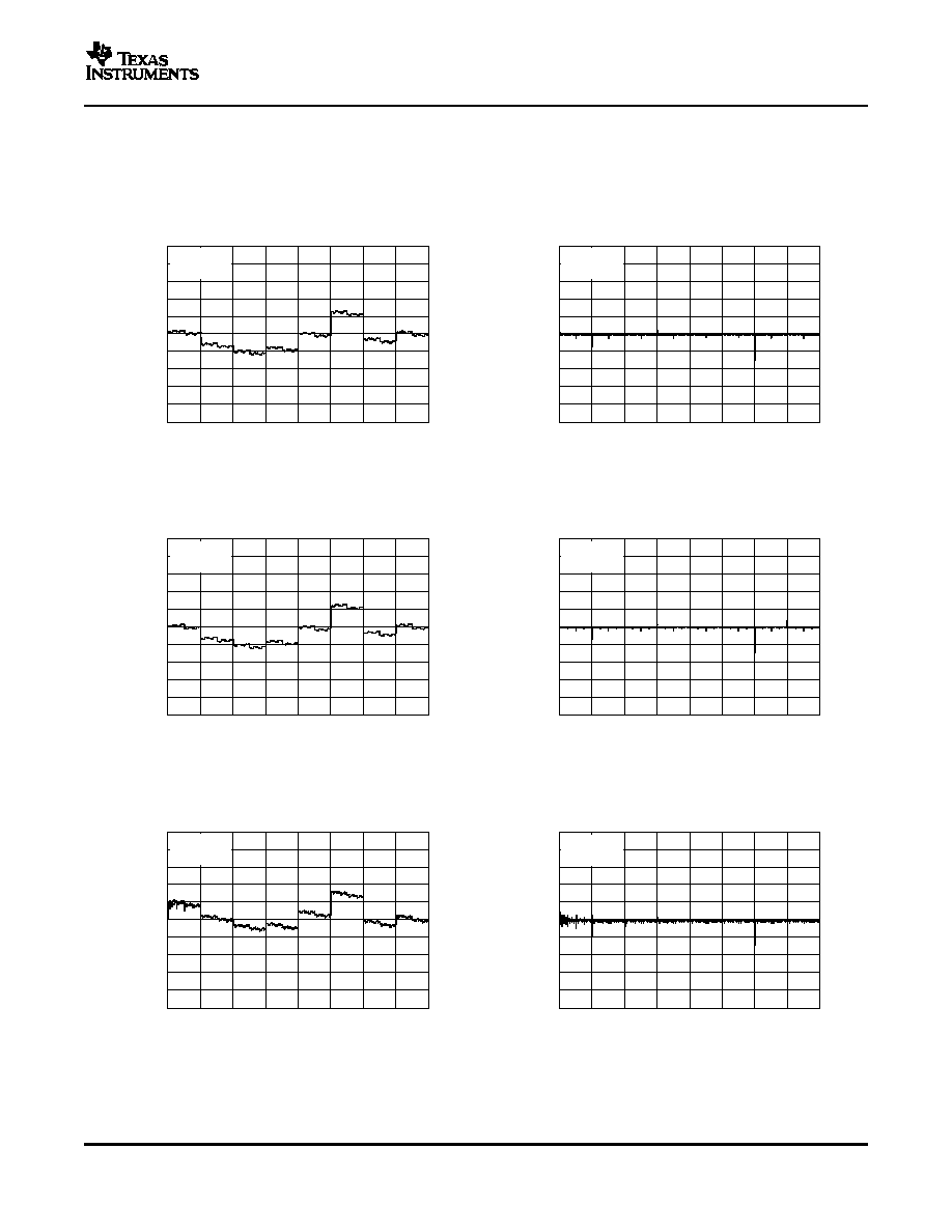
Figure 13.
Figure 14.
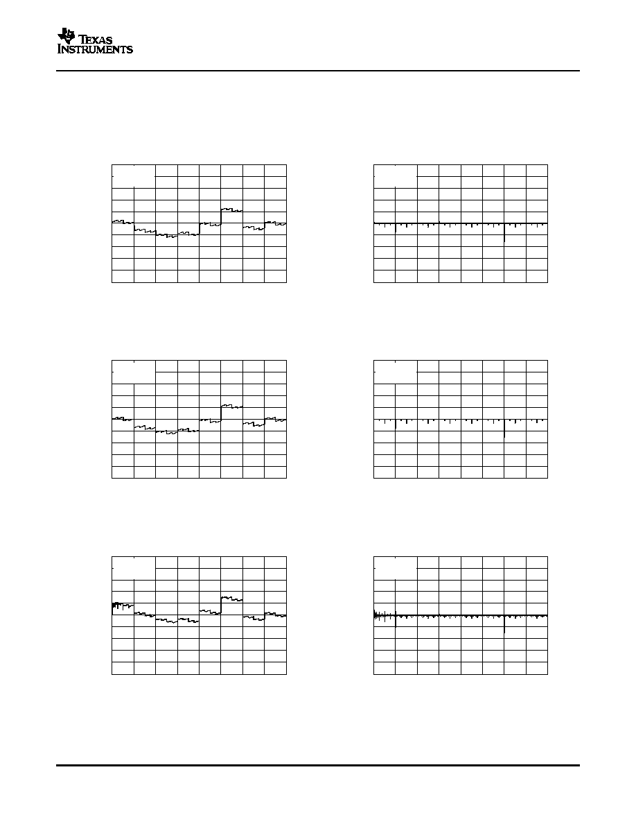
MIDSCALE DAC GLITCH
MIDSCALE DAC GLITCH
Figure 15.
Figure 16.
GAIN ERROR
DAC SETTLING TIME
vs TEMPERATURE
Figure 17.
Figure 18.
8
Submit Documentation Feedback
www.ti.com
2.0
1.8
1.6
1.4
1.2
1.0
0.8
0.6
0.4
0.2
0
QuiescentCurrent(
A)
m
-40
-20
0
20
40
60
80
100
120
Temperature ( C)
∞
V
= +10V
REF
V
= +2.5V
DD
V
= +5.0V
DD
2.0
1.8
1.6
1.4
1.2
1.0
0.8
0.6
0.4
0.2
0
-40
-20
0
20
40
60
80
100
120
OutputLeakage(nA)
Temperature ( C)
∞
V
= +10V
REF
DAC7822
SBAS374 ≠ JUNE 2006
TYPICAL CHARACTERISTICS: V
DD
= +5V (continued)
At T
A
= +25
∞
C, +V
DD
= +5V, unless otherwise noted.
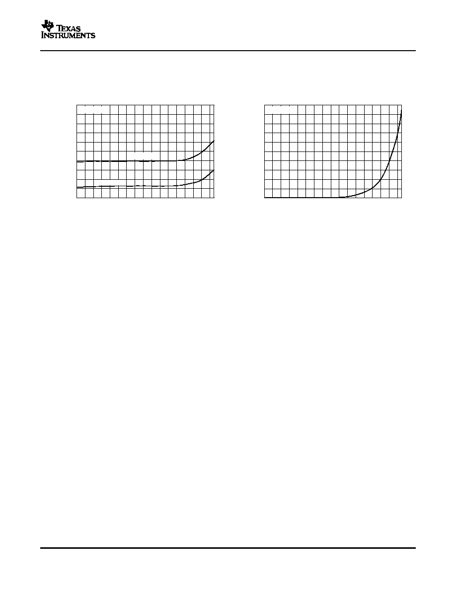
SUPPLY CURRENT
OUTPUT LEAKAGE
vs TEMPERATURE
vs TEMPERATURE
Figure 19.
Figure 20.
9
Submit Documentation Feedback
www.ti.com
TYPICAL CHARACTERISTICS: V
DD
= +2.5V
Channel A
1.0
0.8
0.6
0.4
0.2
0
-0.2
-0.4
-0.6
-0.8
-1.0
0
512
1024
1536
2048
2560
3072
3584
4096
INL(LSB)
Digital Input Code
T = +25 C
∞
A
V
= +10V
REF
1.0
0.8
0.6
0.4
0.2
0
-0.2
-0.4
-0.6
-0.8
-1.0
0
512
1024
1536
2048
2560
3072
3584
4096
DNL(LSB)
Digital Input Code
T
A
= +25∞C
V
= +10V
REF
1.0
0.8
0.6
0.4
0.2
0
-0.2
-0.4
-0.6
-0.8
-1.0
0
512
1024
1536
2048
2560
3072
3584
4096
INL(LSB)
Digital Input Code
T = 40
-
∞
A
C
V
= +10V
REF
1.0
0.8
0.6
0.4
0.2
0
-0.2
-0.4
-0.6
-0.8
-1.0
0
512
1024
1536
2048
2560
3072
3584
4096
DNL(LSB)
Digital Input Code
T
A
= -40∞C
V
= +10V
REF
1.0
0.8
0.6
0.4
0.2
0
-0.2
-0.4
-0.6
-0.8
-1.0
0
512
1024
1536
2048
2560
3072
3584
4096
INL(LSB)
Digital Input Code
T
A
= +125∞C
V
= +10V
REF
1.0
0.8
0.6
0.4
0.2
0
-0.2
-0.4
-0.6
-0.8
-1.0
0
512
1024
1536
2048
2560
3072
3584
4096
DNL(LSB)
Digital Input Code
T
A
= +125∞C
V
= +10V
REF
DAC7822
SBAS374 ≠ JUNE 2006
At T
A
= +25
∞
C, +V
DD
= +2.5V, unless otherwise noted.
LINEARITY ERROR
DIFFERENTIAL LINEARITY ERROR
vs DIGITAL INPUT CODE
vs DIGITAL INPUT CODE
Figure 21.
Figure 22.
LINEARITY ERROR
DIFFERENTIAL LINEARITY ERROR
vs DIGITAL INPUT CODE
vs DIGITAL INPUT CODE
Figure 23.
Figure 24.
LINEARITY ERROR
DIFFERENTIAL LINEARITY ERROR
vs DIGITAL INPUT CODE
vs DIGITAL INPUT CODE
Figure 25.
Figure 26.
10
Submit Documentation Feedback
www.ti.com
Channel B
1.0
0.8
0.6
0.4
0.2
0
-0.2
-0.4
-0.6
-0.8
-1.0
0
512
1024
1536
2048
2560
3072
3584
4096
INL(LSB)
Digital Input Code
T
A
= +25∞C
V
= +10V
REF
1.0
0.8
0.6
0.4
0.2
0
-0.2
-0.4
-0.6
-0.8
-1.0
0
512
1024
1536
2048
2560
3072
3584
4096
DNL(LSB)
Digital Input Code
T
A
= +25∞C
V
= +10V
REF
1.0
0.8
0.6
0.4
0.2
0
-0.2
-0.4
-0.6
-0.8
-1.0
0
512
1024
1536
2048
2560
3072
3584
4096
INL(LSB)
Digital Input Code
T
A
=
∞
-40 C
V
= +10V
REF
1.0
0.8
0.6
0.4
0.2
0
-0.2
-0.4
-0.6
-0.8
-1.0
0
512
1024
1536
2048
2560
3072
3584
4096
DNL(LSB)
Digital Input Code
T
40
-
A
=
∞C
V
= +10V
REF
1.0
0.8
0.6
0.4
0.2
0
-0.2
-0.4
-0.6
-0.8
-1.0
0
512
1024
1536
2048
2560
3072
3584
4096
INL(LSB)
Digital Input Code
T = +125 C
∞
A
V
= +10V
REF
1.0
0.8
0.6
0.4
0.2
0
-0.2
-0.4
-0.6
-0.8
-1.0
0
512
1024
1536
2048
2560
3072
3584
4096
DNL(LSB)
Digital Input Code
T = +125 C
∞
A
V
= +10V
REF
DAC7822
SBAS374 ≠ JUNE 2006
TYPICAL CHARACTERISTICS: V
DD
= +2.5V (continued)
At T
A
= +25
∞
C, +V
DD
= +2.5V, unless otherwise noted.
LINEARITY ERROR
DIFFERENTIAL LINEARITY ERROR
vs DIGITAL INPUT CODE
vs DIGITAL INPUT CODE
Figure 27.
Figure 28.
LINEARITY ERROR
DIFFERENTIAL LINEARITY ERROR
vs DIGITAL INPUT CODE
vs DIGITAL INPUT CODE
Figure 29.
Figure 30.
LINEARITY ERROR
DIFFERENTIAL LINEARITY ERROR
vs DIGITAL INPUT CODE
vs DIGITAL INPUT CODE
Figure 31.
Figure 32.
11
Submit Documentation Feedback

www.ti.com
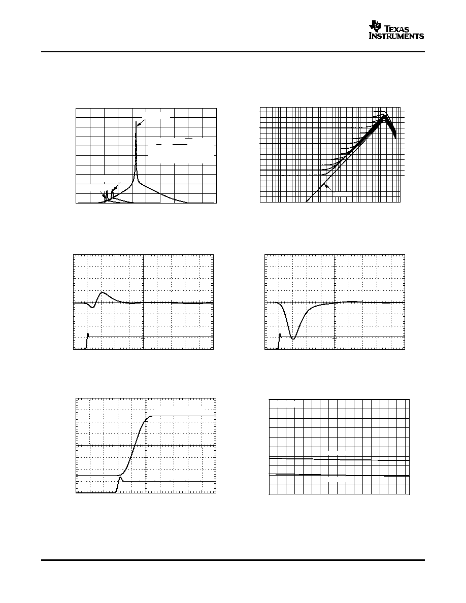
Time (50ns/div)
OutputV
oltage(50mV/div)
Code 2048 to 2047
DAC Update
Time (50ns/div)
OutputV
oltage(50mV/div)
Code 2047 to 2048
DAC Update
GainError(mV)
10
8
6
4
2
0
2
4
6
8
10
-
-
-
-
-
-40
-20
0
20
40
60
80
100
120
Temperature ( C)
∞
V
= +10V
REF
Channel B
Channel A
2.0
1.8
1.6
1.4
1.2
1.0
0.8
0.6
0.4
0.2
0
-40
-20
0
20
40
60
80
100
120
OutputLeakage(nA)
Temperature ( C)
∞
V
= +10V
REF
DAC7822
SBAS374 ≠ JUNE 2006
TYPICAL CHARACTERISTICS: V
DD
= +2.5V (continued)
At T
A
= +25
∞
C, +V
DD
= +2.5V, unless otherwise noted.
MIDSCALE DAC GLITCH
MIDSCALE DAC GLITCH
Figure 33.
Figure 34.
GAIN ERROR
OUTPUT LEAKAGE
vs TEMPERATURE
vs TEMPERATURE
Figure 35.
Figure 36.
12
Submit Documentation Feedback
www.ti.com
THEORY OF OPERATION
R
R
R
R
2R
2R
2R
2R
2R
DB0
(LSB)
DB9
DB10
DB11
(MSB)
I
1
OUT
R
FB
V
REF
I
2
OUT
R
1
V
OUT
+ *
V
REF
CODE
4096
(1)
OPA277
15V
V+
V
-
-15V
GND
I
1
OUT
R
FB
R /R
2
3
V
DD
V
DD
V
OUT
I
2
OUT
R
2
R
3
V
REF
R
1
DAC7822
DAC7822
SBAS374 ≠ JUNE 2006
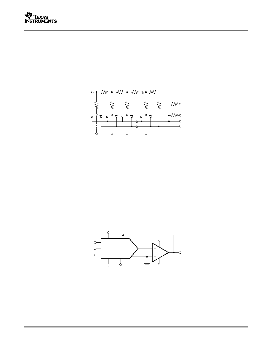
The DAC7822 is a dual channel, current output, 12-bit, digital-to-analog converter (DAC). The architecture,
illustrated in
Figure 37
, is an R-2R ladder configuration with the three MSBs segmented. Each 2R leg of the
ladder is either switched to I
OUT
1 or the I
OUT
2 terminal. The I
OUT
1 terminal of the DAC is held at a virtual GND
potential by the use of an external I/V converter op amp. The R-2R ladder is connected to an external reference
input V
REF
that determines the DAC full-scale current. The R-2R ladder presents a code-independent load
impedance to the external reference of 10k
±
20%. The external reference voltage can vary over a range of
≠15V to +15V, thus providing bipolar I
OUT
current operation. By using an external I/V converter and the
DAC7822 R
FB
resistor, output voltage ranges of ≠V
REF
to V
REF
can be generated.
Figure 37. Equivalent R-2R DAC Circuit
When using an external I/V converter and the DAC7822 R
FB
and R
1
resistors, the DAC output voltage is given
by
Equation 1
:
Each DAC code determines the 2R leg switch position to either GND or I
OUT
. Because the DAC output
impedance as seen looking into the I
OUT
1 terminal changes versus code, the external I/V converter noise gain
also changes. Because of this, the external I/V converter op amp must have a sufficiently low offset voltage such
that the amplifier offset is not modulated by the DAC I
OUT
1 terminal impedance change. External op amps with
large offset voltages can produce INL errors in the transfer function of the DAC7822 as a result of offset
modulation versus DAC code.
For best linearity performance of the DAC7822, a low input offset voltage op amp (such as the OPA277) is
recommended (see
Figure 38
). This circuit allows V
REF
swinging from ≠10V to +10V.
Figure 38. Voltage Output Configuration
13
Submit Documentation Feedback
www.ti.com
APPLICATION INFORMATION
Stability Circuit
GND
I
1
OUT
R
FB
V
REF
V
REF
V
DD
V
DD
V
OUT
I
2
OUT
C
1
U1
DAC7822
Positive Voltage Output Circuit
GND
-
2.5V
+2.5V Reference
OPA277
0
V
<
OUT
+2.5V
<
V
OUT
V
REF
V
DD
V
IN
OPA277
GND
I
1
OUT
R
FB
V
DD
V
OUT
I
2
OUT
C
1
DAC7822
Bipolar Output Section
V
OUT
+
D
0.5
2
N
*
1
V
REF
(2)
DAC7822
SBAS374 ≠ JUNE 2006
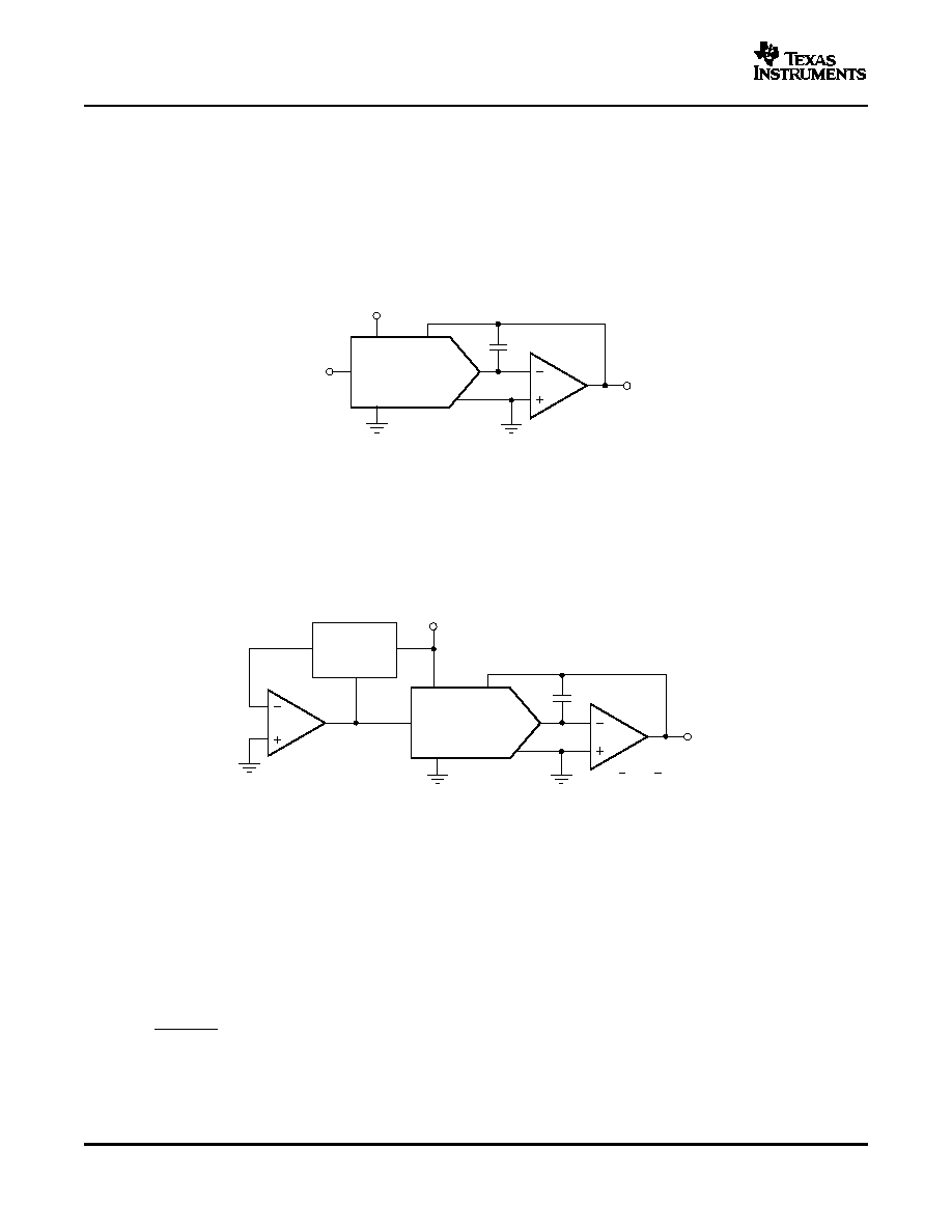
For a current-to-voltage design (see
Figure 39
), the DAC7822 current output (I
OUT
) and the connection with the
inverting node of the op amp should be as short as possible and according to correct printed circuit board (PCB)
layout design. For each code change, there is a step function. If the gain bandwidth product (GBP) of the op
amp is limited and parasitic capacitance is excessive at the inverting node, then gain peaking is possible.
Therefore, for circuit stability, a compensation capacitor C
1
(1pF to 5pF typ) can be added to the design, as
shown in
Figure 39
.
Figure 39. Gain Peaking Prevention Circuit with Compensation Capacitor
As
Figure 40
illustrates, in order to generate a positive voltage output, a negative reference is input to the
DAC7822. This design is suggested instead of using an inverting amp to invert the output as a result of resistor
tolerance errors. For a negative reference, V
OUT
and GND of the reference are level-shifted to a virtual ground
and a ≠2.5V input to the DAC7822 with an op amp.
Figure 40. Positive Voltage Output Circuit
The DAC7822, as a 2-quadrant multiplying DAC, can be used to generate a unipolar output. The polarity of the
full-scale output I
OUT
is the inverse of the input reference voltage at V
REF
.
Some applications require full 4-quadrant multiplying capabilities or bipolar output swing. As shown in
Figure 41
,
external op amp U2 is added as a summing amp and has a gain of 2X that widens the output span to 5V. A
4-quadrant multiplying circuit is implemented by using a 2.5V offset of the reference voltage to bias U2.
According to the circuit transfer equation given in
Equation 2
, input data (D) from code 0 to full-scale produces
output voltages of V
OUT
= ≠2.5V to V
OUT
= +2.5V.
14
Submit Documentation Feedback
www.ti.com
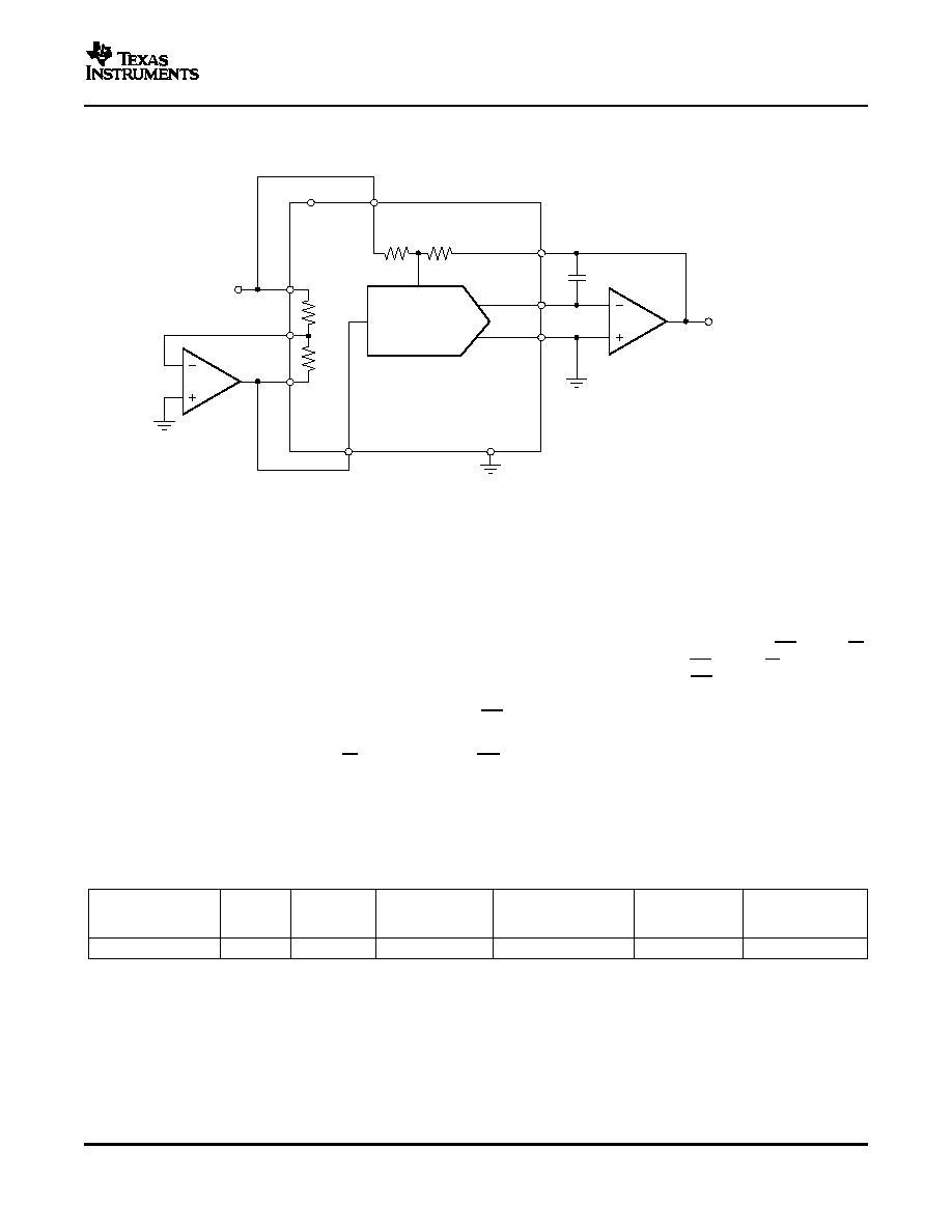
DAC7822
I
1A
OUT
C
1
(2)
V
= V
to +V
-
OUT
IN
IN
AGND
I
2A
OUT
R
1
2R
R
FB
2R
R A
FB
V
DD
V
IN
R
2
2R
R A
2
R
A
2_3
R A
3
R
3
2R
V
A
REF
R A
1
AGND
GND
U2
AGND
U1
NOTES: (1) Similar configuration for DAC B.
(2) C phase compensation (1pF to 5pF) may be
1
required if U2 is a high-speed amplifier.
(1)
Parallel Interface
Cross-Reference
DAC7822
SBAS374 ≠ JUNE 2006
APPLICATION INFORMATION (continued)
External resistance mismatching is the significant error in
Figure 41
.
Figure 41. Bipolar Output Circuit
Data is loaded to the DAC7822 as a 12-bit parallel word. The bi-directional bus is controlled with CS and R/W,
allowing data to be written to or read from the DAC register. To write to the device, CS and R/W are brought
low, and data available on the data lines fills the input register. The rising edge of CS latches the data and
transfers the latched data-word to the DAC register. The DAC latches are not transparent; therefore, a write
sequence must consist of a falling and rising edge on CS in order to ensure that data is loaded to the DAC
register and its analog equivalent is reflected on the DAC output.
To read data stored in the device, R/W is held high and CS is brought low. Data is loaded from the DAC register
back to the input register and out onto the data line, where it can be read back to the controller.
The DAC7822 has an industry-standard pinout.
Table 1
provides the cross-reference information.
Table 1. Cross-Reference
SPECIFIED
TEMPERATURE
PACKAGE
PACKAGE
CROSS-
PRODUCT
INL (LSB)
DNL (LSB)
RANGE
DESCRIPTION
OPTION
REFERENCE PART
DAC7822
±
1
±
1
≠40
∞
C to +125
∞
C
40-Lead QFN
QFN-40
AD5405
15
Submit Documentation Feedback
PACKAGING INFORMATION
Orderable Device
Status
(1)
Package
Type
Package
Drawing
Pins Package
Qty
Eco Plan
(2)
Lead/Ball Finish
MSL Peak Temp
(3)
DAC7822IRTAR
ACTIVE
QFN
RTA
40
2000 Green (RoHS &
no Sb/Br)
CU NIPDAU
Level-2-260C-1 YEAR
DAC7822IRTARG4
ACTIVE
QFN
RTA
40
2000 Green (RoHS &
no Sb/Br)
CU NIPDAU
Level-2-260C-1 YEAR
DAC7822IRTAT
ACTIVE
QFN
RTA
40
250
Green (RoHS &
no Sb/Br)
CU NIPDAU
Level-2-260C-1 YEAR
DAC7822IRTATG4
ACTIVE
QFN
RTA
40
250
Green (RoHS &
no Sb/Br)
CU NIPDAU
Level-2-260C-1 YEAR
(1)
The marketing status values are defined as follows:
ACTIVE: Product device recommended for new designs.
LIFEBUY: TI has announced that the device will be discontinued, and a lifetime-buy period is in effect.
NRND: Not recommended for new designs. Device is in production to support existing customers, but TI does not recommend using this part in
a new design.
PREVIEW: Device has been announced but is not in production. Samples may or may not be available.
OBSOLETE: TI has discontinued the production of the device.
(2)
Eco Plan - The planned eco-friendly classification: Pb-Free (RoHS), Pb-Free (RoHS Exempt), or Green (RoHS & no Sb/Br) - please check
http://www.ti.com/productcontent
for the latest availability information and additional product content details.
TBD: The Pb-Free/Green conversion plan has not been defined.
Pb-Free (RoHS): TI's terms "Lead-Free" or "Pb-Free" mean semiconductor products that are compatible with the current RoHS requirements
for all 6 substances, including the requirement that lead not exceed 0.1% by weight in homogeneous materials. Where designed to be soldered
at high temperatures, TI Pb-Free products are suitable for use in specified lead-free processes.
Pb-Free (RoHS Exempt): This component has a RoHS exemption for either 1) lead-based flip-chip solder bumps used between the die and
package, or 2) lead-based die adhesive used between the die and leadframe. The component is otherwise considered Pb-Free (RoHS
compatible) as defined above.
Green (RoHS & no Sb/Br): TI defines "Green" to mean Pb-Free (RoHS compatible), and free of Bromine (Br) and Antimony (Sb) based flame
retardants (Br or Sb do not exceed 0.1% by weight in homogeneous material)
(3)
MSL, Peak Temp. -- The Moisture Sensitivity Level rating according to the JEDEC industry standard classifications, and peak solder
temperature.
Important Information and Disclaimer:The information provided on this page represents TI's knowledge and belief as of the date that it is
provided. TI bases its knowledge and belief on information provided by third parties, and makes no representation or warranty as to the
accuracy of such information. Efforts are underway to better integrate information from third parties. TI has taken and continues to take
reasonable steps to provide representative and accurate information but may not have conducted destructive testing or chemical analysis on
incoming materials and chemicals. TI and TI suppliers consider certain information to be proprietary, and thus CAS numbers and other limited
information may not be available for release.
In no event shall TI's liability arising out of such information exceed the total purchase price of the TI part(s) at issue in this document sold by TI
to Customer on an annual basis.
PACKAGE OPTION ADDENDUM
www.ti.com
18-Jul-2006
Addendum-Page 1

IMPORTANT NOTICE
Texas Instruments Incorporated and its subsidiaries (TI) reserve the right to make corrections, modifications,
enhancements, improvements, and other changes to its products and services at any time and to discontinue
any product or service without notice. Customers should obtain the latest relevant information before placing
orders and should verify that such information is current and complete. All products are sold subject to TI's terms
and conditions of sale supplied at the time of order acknowledgment.
TI warrants performance of its hardware products to the specifications applicable at the time of sale in
accordance with TI's standard warranty. Testing and other quality control techniques are used to the extent TI
deems necessary to support this warranty. Except where mandated by government requirements, testing of all
parameters of each product is not necessarily performed.
TI assumes no liability for applications assistance or customer product design. Customers are responsible for
their products and applications using TI components. To minimize the risks associated with customer products
and applications, customers should provide adequate design and operating safeguards.
TI does not warrant or represent that any license, either express or implied, is granted under any TI patent right,
copyright, mask work right, or other TI intellectual property right relating to any combination, machine, or process
in which TI products or services are used. Information published by TI regarding third-party products or services
does not constitute a license from TI to use such products or services or a warranty or endorsement thereof.
Use of such information may require a license from a third party under the patents or other intellectual property
of the third party, or a license from TI under the patents or other intellectual property of TI.
Reproduction of information in TI data books or data sheets is permissible only if reproduction is without
alteration and is accompanied by all associated warranties, conditions, limitations, and notices. Reproduction
of this information with alteration is an unfair and deceptive business practice. TI is not responsible or liable for
such altered documentation.
Resale of TI products or services with statements different from or beyond the parameters stated by TI for that
product or service voids all express and any implied warranties for the associated TI product or service and
is an unfair and deceptive business practice. TI is not responsible or liable for any such statements.
Following are URLs where you can obtain information on other Texas Instruments products and application
solutions:
Products
Applications
Amplifiers
amplifier.ti.com
Audio
www.ti.com/audio
Data Converters
dataconverter.ti.com
Automotive
www.ti.com/automotive
DSP
dsp.ti.com
Broadband
www.ti.com/broadband
Interface
interface.ti.com
Digital Control
www.ti.com/digitalcontrol
Logic
logic.ti.com
Military
www.ti.com/military
Power Mgmt
power.ti.com
Optical Networking
www.ti.com/opticalnetwork
Microcontrollers
microcontroller.ti.com
Security
www.ti.com/security
Low Power Wireless www.ti.com/lpw
Telephony
www.ti.com/telephony
Video & Imaging
www.ti.com/video
Wireless
www.ti.com/wireless
Mailing Address:
Texas Instruments
Post Office Box 655303 Dallas, Texas 75265
Copyright
2006, Texas Instruments Incorporated