Burr Brown Products
from Texas Instruments
FEATURES
DESCRIPTION
APPLICATIONS
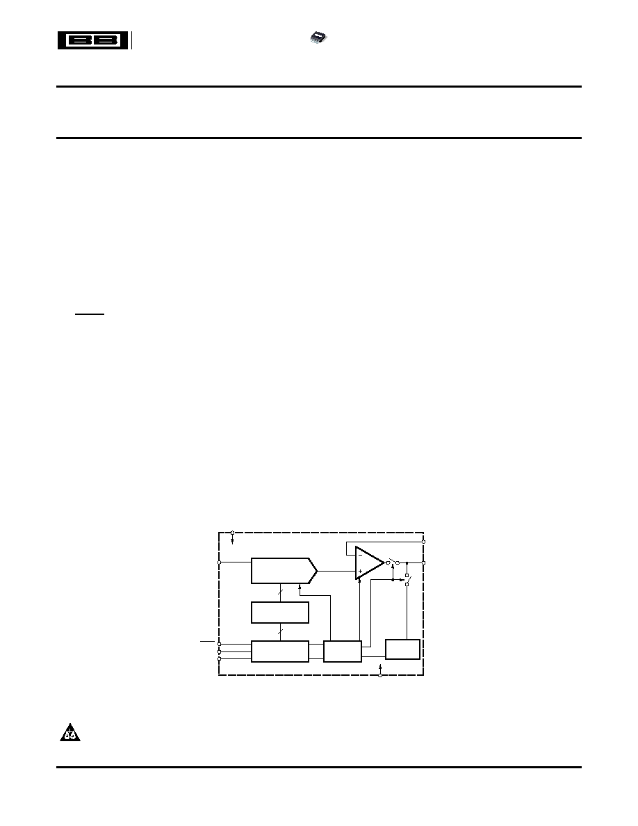
Shift Register
16
DAC Register
16
16-Bit DAC
Ref (+)
Resistor
Networ
k
V
DD
GND
V
OUT
V
FB
SYNC
V
REF
SCLK
D
IN
PWD Control
DAC8551
SLAS429A ≠ APRIL 2005 ≠ REVISED JULY 2005
16-BIT, ULTRA-LOW GLITCH, VOLTAGE OUTPUT
DIGITAL-TO-ANALOG CONVERTER
∑
16-Bit Monotonic Over Temperature
The DAC8551 is a small, low-power, voltage output,
16-bit
digital-to-analog
converter
(DAC).
It
is
∑
Relative Accuracy: 8 LSB (Max)
monotonic, provides good linearity, and minimizes
∑
Glitch Energy: 0.1 nV-s
undesired
code-to-code
transient
voltages.
The
∑
Settling Time: 10 µs to
±
0.003% FSR
DAC8551 uses a versatile 3-wire serial interface that
∑
Power Supply: +2.7 V to +5.5 V
operates at clock rates to 30 MHz and is compatible
with standard SPITM, QSPITM, MicrowireTM, and digital
∑
MicroPower Operation: 200 µA at 5 V
signal processor (DSP) interfaces.
∑
Rail-to-Rail Output Amplifier
The DAC8551 requires an external reference voltage
∑
Power-On Reset to Zero
to set its output range. The DAC8551 incorporates a
∑
Power-Down Capability
power-on-reset circuit that ensures the DAC output
∑
Schmitt-Triggered Digital Inputs
powers up at 0 V and remains there until a valid write
takes place to the device. The DAC8551 contains a
∑
SYNC Interrupt Facility
power-down
feature,
accessed
over
the
serial
∑
Drop-In Compatible With DAC8531/01
interface, that reduces the current consumption of the
∑
Operating Temperature Range: -40
∞
C to 105
∞
C
device to 200 nA at 5 V.
∑
Available Package:
The low-power consumption of this device in normal
≠ 3 mm
◊
5 mm MSOP-8
operation makes it ideally suited for portable battery-
operated equipment. The power consumption is
1.00 mW at 5 V, reducing to 1 µW in power-down
mode.
∑
Process Control
The DAC8551 is available in an MSOP-8 package.
∑
Data Acquisition Systems
∑
Closed-Loop Servo-Control
∑
PC Peripherals
∑
Portable Instrumentation
∑
Programmable Attenuation
FUNCTIONAL BLOCK DIAGRAM
Please be aware that an important notice concerning availability, standard warranty, and use in critical applications of Texas
Instruments semiconductor products and disclaimers thereto appears at the end of this data sheet.
SPI, QSPI are trademarks of Motorola.
Microwire is a trademark of National Semiconductor.
PRODUCTION DATA information is current as of publication date.
Copyright © 2005, Texas Instruments Incorporated
Products conform to specifications per the terms of the Texas
Instruments standard warranty. Production processing does not
necessarily include testing of all parameters.
www.ti.com
ABSOLUTE MAXIMUM RATINGS
(1)
ELECTRICAL CHARACTERISTICS
DAC8551
SLAS429A ≠ APRIL 2005 ≠ REVISED JULY 2005
This integrated circuit can be damaged by ESD. Texas Instruments recommends that all integrated
circuits be handled with appropriate precautions. Failure to observe proper handling and installation
procedures can cause damage.
ESD damage can range from subtle performance degradation to complete device failure. Precision
integrated circuits may be more susceptible to damage because very small parametric changes could
cause the device not to meet its published specifications.
PACKAGING/ORDERING INFORMATION
MINIMUM
DIFFERENTIAL
SPECIFICATION
TRANSPORT
RELATIVE
PACKAGE
PACKAGE
PACKAGE
ORDERING
PRODUCT
NONLINEARITY
TEMPERATURE
MEDIA,
ACCURACY
LEAD
DESIGNATOR
(1)
MARKING
NUMBER
(LSB)
RANGE
QUANTITY
(LSB)
DAC8551IDGK
Tube, 80
DAC8551I
±
8
±
1
MSOP-8
DGK
≠40
∞
C TO 105
∞
C
D81
DAC8551IDGKT
Tape and Reel, 250
DAC8551IDGKR
Tape and Reel, 2500
(1)
For the most current specifications and package information, refer to our web site at www.ti.com.
UNIT
V
DD
to GND
≠0.3 V to 6 V
Digital input voltage to GND
≠0.3 V to +V
DD
+ 0.3 V
V
OUT
to GND
≠0.3 V to +V
DD
+ 0.3 V
Operating temperature range
≠40
∞
C to 105
∞
C
Storage temperature range
≠65
∞
C to 150
∞
C
Junction temperature range (T
J
max)
150
∞
C
Power dissipation (DGK)
(T
J
max ≠ T
A
)/
JA
JA
Thermal impedance
206
∞
C/W
JC
Thermal impedance
44
∞
C/W
Vapor phase (60 s)
215
∞
C
Lead temperature, soldering
Infrared (15 s)
220
∞
C
(1)
Stresses above those listed under absolute maximum ratings may cause permanent damage to the device. Exposure to absolute
maximum conditions for extended periods may affect device reliability.
V
DD
= 2.7 V to 5.5 V,≠ 40
∞
C to 105
∞
C range (unless otherwise noted)
PARAMETER
TEST CONDITIONS
MIN
TYP
MAX
UNIT
STATIC PERFORMANCE
(1)
Resolution
16
Bits
Relative accuracy
Measured by line passing through codes 485 and 64741
±
3
±
8
LSB
Differential nonlinearity
16-bit Monotonic
±
0.25
±
1
LSB
Zero-code error
±
2
±
12
mV
Full-scale error
Measured by line passing through codes 485 and 64741.
±
0.05
±
0.5
% of FSR
Gain error
±
0.02
±
0.15
% of FSR
Zero-code error drift
±
5
µV/
∞
C
Gain temperature coefficient
±
1
ppm of FSR/
∞
C
8
mV
Power supply rejection ratio
R
L
= 2 k
, C
L
= 200 pF
(PSRR)
0.75
mV/V
(1)
Linearity calculated using a reduced code range of 485 to 64741; output unloaded.
2
www.ti.com
DAC8551
SLAS429A ≠ APRIL 2005 ≠ REVISED JULY 2005
ELECTRICAL CHARACTERISTICS (continued)
V
DD
= 2.7 V to 5.5 V,≠ 40
∞
C to 105
∞
C range (unless otherwise noted)
PARAMETER
TEST CONDITIONS
MIN
TYP
MAX
UNIT
OUTPUT CHARACTERISTICS
(2)
Output voltage range
0
V
REF
V
To
±
0.003% FSR, 0200
H
to FD00
H
, R
L
= 2 k
, 0 pF < C
L
<
8
10
µs
200 pF
Output voltage settling time
R
L
= 2 k
, C
L
= 500 pF
12
µs
Slew rate
1.8
V/µs
R
L
=
470
pF
Capacitive load stability
R
L
= 2 k
1000
pF
Code change glitch impulse
1 LSB change around major carry
0.1
nV-s
Digital feedthrough
SCLK toggling, FSYNC high
0.1
DC output impedance
At mid-code input
1
V
DD
= 5 V
50
Short-circuit current
mA
V
DD
= 3 V
20
Coming out of power-down mode V
DD
= 5 V
2.5
Power-up time
µs
Coming out of power-down mode V
DD
= 3 V
5
AC PERFORMANCE
SNR (1st 19 harmonics removed)
95
THD
85
BW = 20 kHz, V
DD
= 5 V, F
OUT
= 1 kHz
dB
SFDR
87
SINAD
84
REFERENCE INPUT
V
REF
Voltage
0
V
DD
V
V
REF
= V
DD
= 5 V
50
75
µA
Reference input range
V
REF
= V
DD
= 3.6 V
30
45
µA
Reference input impedance
125
k
LOGIC INPUTS
(3)
Input current
±
1
µA
V
DD
= 5 V
0.8
V
IN
L
Logic input LOW voltage
V
V
DD
= 3 V
0.6
V
DD
= 5 V
2.4
V
IN
H
Logic input HIGH voltage
V
V
DD
= 3 V
2.1
Pin capacitance
3
pF
POWER REQUIREMENTS
V
DD
2.7
5.5
V
I
DD
(normal mode)
Input code = 32768, reference current included, no load
V
DD
= 3.6 V to 5.5 V
200
250
V
IH
= V
DD
and V
IL
= GND
µA
V
DD
= 2.7 V to 3.6 V
180
240
I
DD
(all power-down modes)
V
DD
= 3.6 V to 5.5 V
V
IH
= V
DD
and V
IL
= GND
0.2
1
µA
V
DD
= 2.7 V to 3.6 V
0.05
1
POWER EFFICIENCY
I
OUT
/I
DD
I
LOAD
= 2 mA, V
DD
= 5 V
89%
TEMPERATURE RANGE
Specified performance
≠40
105
∞
C
(2)
Ensured by design and characterization, not production tested.
(3)
Ensured by design and characterization, not production tested.
3
www.ti.com
PIN CONFIGURATION
V
DD
V
REF
V
FB
V
OUT
GND
D
IN
SCLK
SYNC
1
2
3
4
8
7
6
5
DAC8551
DAC8551
SLAS429A ≠ APRIL 2005 ≠ REVISED JULY 2005
MSOP-8
(Top View)
PIN DESCRIPTIONS
PIN
NAME
DESCRIPTION
1
V
DD
Power supply input, 2.7 V to 5.5 V.
2
V
REF
Reference voltage input.
3
V
FB
Feedback connection for the output amplifier. For voltage output operation, tie to V
OUT
externally.
4
V
OUT
Analog output voltage from DAC. The output amplifier has rail-to-rail operation.
Level-triggered control input (active LOW). This is the frame synchronization signal for the input data. When SYNC goes
LOW, it enables the input shift register and data is transferred in on the falling edges of the following clocks. The DAC is
5
SYNC
updated following the 24th clock (unless SYNC is taken HIGH before this edge in which case the rising edge of SYNC acts
as an interrupt and the write sequence is ignored by the DAC8551).
6
SCLK
Serial clock input. Data can be transferred at rates up to 30 MHz.
7
D
IN
Serial data input. Data is clocked into the 24-bit input shift register on each falling edge of the serial clock input.
8
GND
Ground reference point for all circuitry on the part.
4
www.ti.com
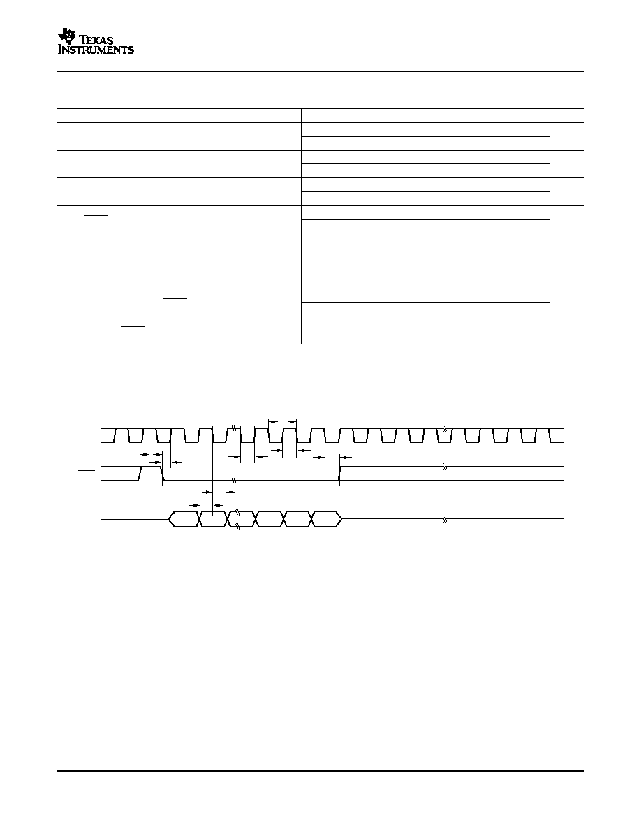
TIMING REQUIREMENTS
(1) (2)
SERIAL WRITE OPERATION
SCLK
SYNC
D
IN
DB23
DB0
t
8
t
3
t
2
t
7
t
4
t
5
t
6
t
1
DAC8551
SLAS429A ≠ APRIL 2005 ≠ REVISED JULY 2005
V
DD
= 2.7 V to 5.5 V, all specifications ≠40
∞
C to 105
∞
C (unless otherwise noted)
PARAMETER
TEST CONDITIONS
MIN
TYP
MAX
UNIT
V
DD
= 2.7 V to 3.6 V
50
t
1
(3)
SCLK cycle time
ns
V
DD
= 3.6 V to 5.5 V
33
V
DD
= 2.7 V to 3.6 V
13
t
2
SCLK HIGH time
ns
V
DD
= 3.6 V to 5.5 V
13
V
DD
= 2.7 V to 3.6 V
22.5
t
3
SCLK LOW time
ns
V
DD
= 3.6 V to 5.5 V
13
V
DD
= 2.7 V to 3.6 V
0
t
4
SYNC to SCLK rising edge setup time
ns
V
DD
= 3.6 V to 5.5 V
0
V
DD
= 2.7 V to 3.6 V
5
t
5
Data setup time
ns
V
DD
= 3.6 V to 5.5 V
5
V
DD
= 2.7 V to 3.6 V
4.5
t
6
Data hold time
ns
V
DD
= 3.6 V to 5.5 V
4.5
V
DD
= 2.7 V to 3.6 V
0
t
7
SCLK falling edge to SYNC rising edge
ns
V
DD
= 3.6 V to 5.5 V
0
V
DD
= 2.7 V to 3.6 V
50
t
8
Minimum SYNC HIGH time
ns
V
DD
= 3.6 V to 5.5 V
33
(1)
All input signals are specified with t
R
= t
F
= 3 ns (10% to 90% of V
DD
) and timed from a voltage level of (V
IL
+ V
IH
)/2.
(2)
See Serial Write Operation timing diagram.
(3)
Maximum SCLK frequency is 30 MHz at V
DD
= 3.6 V to 5.5 V and 20 MHz at V
DD
= 2.7 V to 3.6 V.
5
www.ti.com
TYPICAL CHARACTERISTICS: V
DD
= 5 V
-6
-4
-2
0
2
4
6
LE - (LSB)
-1
-0.5
0
0.5
1
0
8192
16384
24576 32768
40960
49152 57344 65536
Digital Input Code
DLE - (LSB)
V
DD
= 5 V, V
REF
= 4.99 V
-6
-4
-2
0
2
4
6
LE - (LSB)
-1
-0.5
0
0.5
1
0
8192
16384
24576
32768 40960 49152
57344 65536
Digital Input Code
DLE - (LSB)
V
DD
= 5 V, V
REF
= 4.99 V
-6
-4
-2
0
2
4
6
LE - (LSB)
-1
-0.5
0
0.5
1
0
8192
16384 24576
32768
40960
49152 57344 65536
Digital Input Code
DLE - (LSB)
V
DD
= 5 V, V
REF
= 4.99 V
-5
0
5
10
-40
0
40
80
120
Temperature -
5
C
Error (mV)
V
DD
= 5 V, V
REF
= 4.99 V
0
200
400
600
800
1000
120
140
160
180
200
220
240
260
280
300
I
DD
- Supply Current -
m
A
f - Frequency - Hz
V
DD
= V
REF
= 5.5 V,
Reference Current Included
-10
-5
0
-40
0
40
80
120
Temperature -
5
C
Error (mV)
V
DD
= 5 V, V
REF
= 4.99 V
DAC8551
SLAS429A ≠ APRIL 2005 ≠ REVISED JULY 2005
At T
A
= 25
∞
C, unless otherwise noted
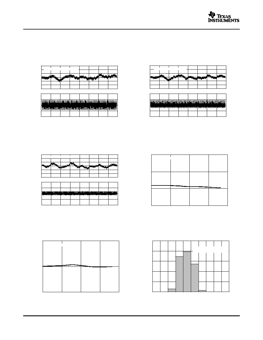
LINEARITY ERROR AND
LINEARITY ERROR AND
DIFFERENTIAL LINEARITY ERROR vs DIGITAL INPUT
DIFFERENTIAL LINEARITY ERROR vs DIGITAL INPUT
CODE
CODE
(-40
∞
C)
(25
∞
C)
Figure 1.
Figure 2.
LINEARITY ERROR AND
ZERO-SCALE ERROR
DIFFERENTIAL LINEARITY ERROR vs DIGITAL INPUT
vs
CODE
TEMPERATURE
(105
∞
C)
Figure 3.
Figure 4.
FULL-SCALE ERROR
I
DD
HISTOGRAM
vs
TEMPERATURE
Figure 5.
Figure 6.
6
www.ti.com
I
(SOURCE/SINK)
- mA
0
1
2
3
4
5
6
0
3
5
8
10
- Output V
oltage - V
V
OUT
DAC Loaded With 0000
H
DAC Loaded With FFFF
H
V
DD
= 5.5 V
V
REF
= V
DD
-10 mV
0
50
100
150
200
250
300
0
8192
16384 24576
32768 40960
49152 57344 65536
Digital Input Code
DDI
Supply Current -
-
A
µ
V
DD
= V
REF
= 5.5 V
Reference Current Included
Quiescent Current -
A
µ
0
50
100
150
200
250
-40
-10
20
50
80
110
Temperature -
5
C
V
DD
= V
REF
= 5.5 V
Reference Current Included
100
120
140
160
180
200
220
240
260
280
300
2.7
3.1
3.4
3.8
4.1
4.5
4.8
5.2
5.5
DDI
Supply Current -
-
A
µ
V
DD
- Supply Voltage - V
V
REF
= V
DD
Reference Current Include, No Load
0
0.3
0.5
0.8
1
2.7
3.1
3.4
3.8
4.1
4.5
4.8
5.2
5.5
I
A
µ
V
DD
- Supply Voltage - V
V
REF
= V
DD
DD
- Supply Current -
100
500
900
1300
1700
0
1
2
3
4
5
DDI
Supply Current -
-
A
µ
V
DD
= V
REF
= 5.5 V
T
A
= 25
∞
C, SCL Input (All Other Inputs = GND)
V
(LOGIC)
- V
DAC8551
SLAS429A ≠ APRIL 2005 ≠ REVISED JULY 2005
TYPICAL CHARACTERISTICS: V
DD
= 5 V (continued)
At T
A
= 25
∞
C, unless otherwise noted
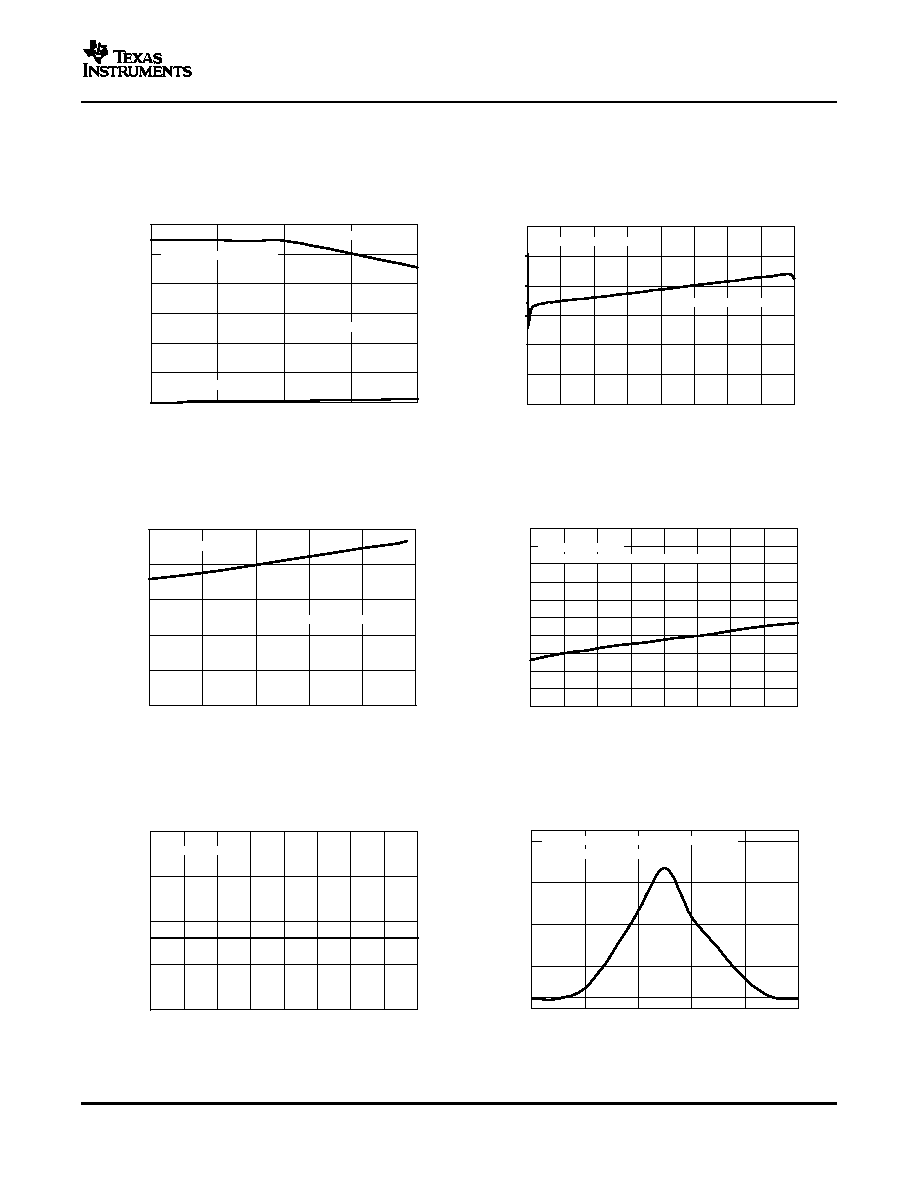
SOURCE AND SINK CURRENT CAPABILITY
SUPPLY CURRENT
vs
DIGITAL INPUT CODE
Figure 7.
Figure 8.
POWER-SUPPLY CURRENT
SUPPLY CURRENT
vs
vs
TEMPERATURE
SUPPLY VOLTAGE
Figure 9.
Figure 10.
POWER-DOWN CURRENT
SUPPLY CURRENT
vs
vs
SUPPLY VOLTAGE
LOGIC INPUT VOLTAGE
Figure 11.
Figure 12.
7
www.ti.com
Time (2
µ
s/div)
V
DD
= 5 V,
V
REF
= 4.096 V,
From Code: FFFF
To Code: 0000
Zoomed Falling Edge
1 mV/div
Trigger Pulse
5 V/div
Falling
Edge
1 V/div
Time (2
µ
s/div)
V
DD
= 5 V,
V
REF
= 4.096 V,
From Code: 0000
To Code: FFFF
Zoomed Rising Edge
1 mV/div
Trigger Pulse
5 V/div
Rising Edge
1 V/div
Time (2
µ
s/div)
V
DD
= 5 V,
V
REF
= 4.096 V,
From Code: 4000
To Code: CFFF
Zoomed Rising Edge
1 mV/div
Trigger Pulse
5 V/div
Rising
Edge
1 V/div
Time (2
µ
s/div)
V
DD
= 5 V,
V
REF
= 4.096 V,
From Code: CFFF
To Code: 4000
Zoomed Falling Edge
1 mV/div
Trigger Pulse
5 V/div
Falling
Edge
1 V/div
V
DD
= 5 V,
V
REF
= 4.096 V
From Code: 8000
To Code: 7FFF
Glitch: 0.16 nV-s
Measured Worst Case
Time 400 ns/div
V
OUT
(500
m
V/div)
V
DD
= 5 V,
V
REF
= 4.096 V
From Code: 7FFF
To Code: 8000
Glitch: 0.08 nV-s
Time 400 ns/div
V
OUT
(500
m
V/div)
DAC8551
SLAS429A ≠ APRIL 2005 ≠ REVISED JULY 2005
TYPICAL CHARACTERISTICS: V
DD
= 5 V (continued)
At T
A
= 25
∞
C, unless otherwise noted
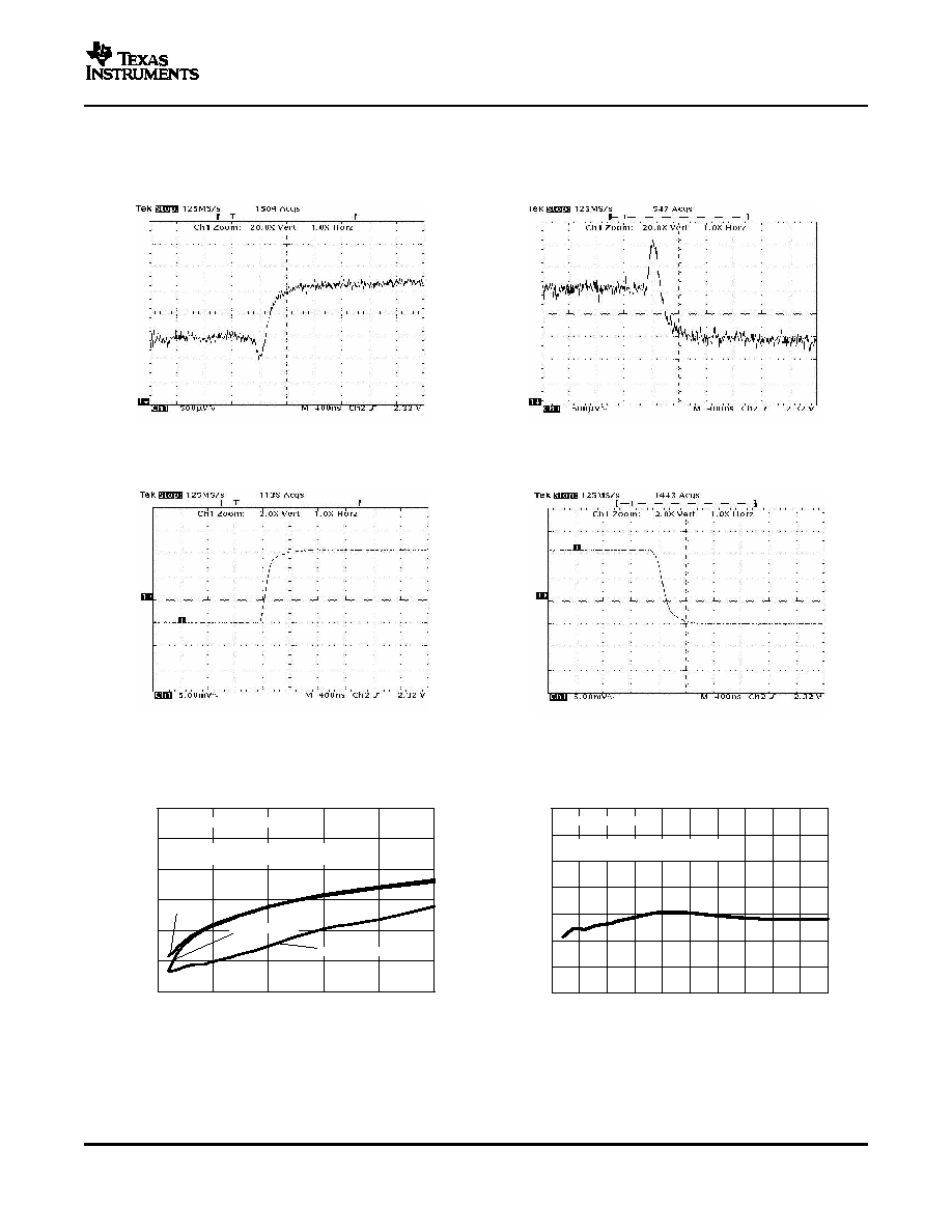
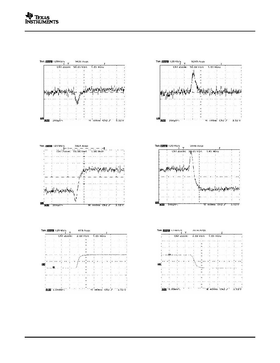
FULL-SCALE SETTLING TIME: 5-V RISING EDGE
FULL-SCALE SETTLING TIME: 5-V FALLING EDGE
Figure 13.
Figure 14.
HALF-SCALE SETTLING TIME: 5-V RISING EDGE
HALF-SCALE SETTLING TIME: 5-V FALLING EDGE
Figure 15.
Figure 16.
GLITCH ENERGY: 5-V, 1-LSB STEP, RISING EDGE
GLITCH ENERGY: 5-V, 1-LSB STEP, FALLING EDGE
Figure 17.
Figure 18.
8
www.ti.com
V
DD
= 5 V,
V
REF
= 4.096 V
From Code: 8010
To Code: 8000
Glitch: 0.08 nV-s
Time 400 ns/div
V
OUT
(500
V/div)
m
V
DD
= 5 V,
V
REF
= 4.096 V
From Code: 8000
To Code: 8010
Glitch: 0.04 nV-s
Time 400 ns/div
V
OUT
(500
m
V/div)
V
DD
= 5 V,
V
REF
= 4.096 V
From Code: 80FF
To Code: 8000
Glitch: Not Detected
Theoretical Worst Case
Time 400 ns/div
V
OUT
(5 mV/div)
V
DD
= 5 V,
V
REF
= 4.096 V
From Code: 8000
To Code: 80FF
Glitch: Not Detected
Theoretical Worst Case
Time 400 ns/div
V
OUT
(5 mV/div)
84
86
88
90
92
94
96
98
0
0.5
1
1.5
2
2.5
3
3.5
4
4.5
5
SNR - Signal-to-Noise Ratio - dB
f - Output Frequency - kHz
V
DD
= V
REF
= 5 V
-1 dB FSR Digital Input, Fs = 1 MSPS
Measurement Bandwidth = 20 kHz
-100
-90
-80
-70
-60
-50
-40
0
1
2
3
4
5
THD - T
otal Harmonic Distortion - dB
Output Tone - kHz
THD
2nd Harmonic
3rd Harmonic
-1dB FSR Digital Input, Fs = 1 MSPS
Measurement Bandwidth = 20 kHz
V
DD
= 5 V, V
REF
= 4.9 V
DAC8551
SLAS429A ≠ APRIL 2005 ≠ REVISED JULY 2005
TYPICAL CHARACTERISTICS: V
DD
= 5 V (continued)
At T
A
= 25
∞
C, unless otherwise noted
GLITCH ENERGY: 5-V, 16-LSB STEP, RISING EDGE
GLITCH ENERGY: 5-V, 16-LSB STEP, FALLING EDGE
Figure 19.
Figure 20.
GLITCH ENERGY: 5-V, 256-LSB STEP, RISING EDGE
GLITCH ENERGY: 5-V, 256-LSB STEP, FALLING EDGE
Figure 21.
Figure 22.
TOTAL HARMONIC DISTORTION
SIGNAL-TO-NOISE RATIO
vs
vs
OUTPUT FREQUENCY
OUTPUT FREQUENCY
Figure 23.
Figure 24.
9
www.ti.com
100
150
200
250
300
350
100
1000
10000
100000
V
DD
= 5 V
V
REF
= 4.096
Code = 7FFF
No Load
nV/
Hz
- V
oltage Noise -
V
n
f - Frequency - Hz
-130
-110
-90
-70
-50
-30
-10
0
5000
10000
15000
20000
V
DD
= 5.0 V, V
REF
= 4.096 V
f
OUT
= 1 kHz
f
CLK
=
1 MSPS
f - Frequency - Hz
Gain - dB
TYPICAL CHARACTERISTICS: V
DD
= 2.7 V
-6
-4
-2
0
2
4
6
LE - (LSB)
-1
-0.5
0
0.5
1
0
8192
16384
24576
32768 40960
49152 57344 65536
Digital Input Code
DLE - (LSB)
V
DD
= 2.7 V, V
REF
= 2.69 V
-6
-4
-2
0
2
4
6
LE - (LSB)
DLE - (LSB)
V
DD
= 2.7 V, V
REF
= 2.69 V
-1
-0.5
0
0.5
1
0
8192
16384
24576 32768 40960
49152 57344 65536
Digital Input Code
DAC8551
SLAS429A ≠ APRIL 2005 ≠ REVISED JULY 2005
TYPICAL CHARACTERISTICS: V
DD
= 5 V (continued)
At T
A
= 25
∞
C, unless otherwise noted
POWER SPECTRAL DENSITY
OUTPUT NOISE DENSITY
Figure 25.
Figure 26.
At T
A
= 25
∞
C, unless otherwise noted
LINEARITY ERROR AND
LINEARITY ERROR AND
DIFFERENTIAL LINEARITY ERROR vs DIGITAL
DIFFERENTIAL LINEARITY ERROR vs DIGITAL
INPUT CODE
INPUT CODE
(-40
∞
C)
(25
∞
C)
Figure 27.
Figure 28.
10
www.ti.com
-6
-4
-2
0
2
4
6
LE - (LSB)
V
DD
= 2.7 V, V
REF
= 2.69 V
-1
-0.5
0
0.5
1
0
8192
16384
24576
32768
40960
49152 57344 65536
Digital Input Code
DLE - (LSB)
-5
0
5
10
-40
0
40
80
120
Temperature -
5
C
Error (mV)
V
DD
= 2.7 V, V
REF
= 2.69 V
0
300
600
900
1200
1500
120
140
160
180
200
220
240
260
280
300
I
DD
- Supply Current -
m
A
f - Frequency - Hz
V
DD
= V
REF
= 2.7 V
Reference Current Included
-10
-5
0
5
-40
0
40
80
120
Temperature -
5
C
Error (mV)
V
DD
= 2.7 V, V
REF
= 2.69 V
0
0.5
1
1.5
2
2.5
3
0
3
5
8
10
I
(SOURCE/SINK)
- mA
- Output V
oltage - V
V
OUT
DAC Loaded With 0000
H
DAC Loaded With FFFF
H
V
DD
= 2.7 V
V
REF
= V
DD
- 10 mV
0
20
40
60
80
100
120
140
160
180
0
8192
16384
24576 32768
40960
49152
57344
65536
Digital Input Code
DDI
Supply Current -
-
A
µ
V
DD
= V
REF
= 2.7 V
Reference Current Included
DAC8551
SLAS429A ≠ APRIL 2005 ≠ REVISED JULY 2005
TYPICAL CHARACTERISTICS: V
DD
= 2.7 V (continued)
At T
A
= 25
∞
C, unless otherwise noted
LINEARITY ERROR AND
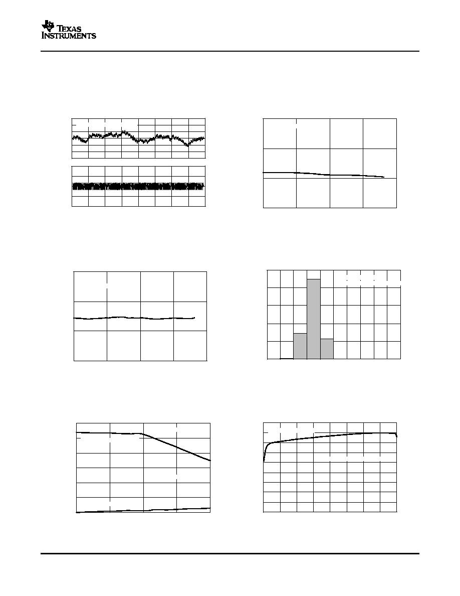
ZERO-SCALE ERROR
DIFFERENTIAL LINEARITY ERROR vs DIGITAL INPUT
vs
CODE
TEMPERATURE
(105
∞
C)
Figure 29.
Figure 30.
FULL-SCALE ERROR
I
DD
HISTOGRAM
vs
TEMPERATURE
Figure 31.
Figure 32.
SOURCE AND SINK CURRENT CAPABILITY
SUPPLY CURRENT
vs
DIGITAL INPUT CODE
Figure 33.
Figure 34.
11
www.ti.com
100
300
500
700
0
0.5
1
1.5
2
2.5
DDI
Supply Current -
-
A
µ
V
DD
= V
REF
= 2.7 V
T
A
= 25
∞
C, SCL Input (All Other Inputs = GND)
V
(LOGIC)
- V
0
50
100
150
200
250
-40
-10
20
50
80
110
Quiescent Current -
A
µ
Temperature -
5
C
V
DD
= V
REF
= 2.7 V
Reference Current Included
Time (2
µ
s/div)
V
DD
= 2.7 V,
V
REF
= 2.5 V,
From Code: 0000
To Code: FFFF
Zoomed Rising Edge
1 mV/div
Trigger Pulse
2.7 V/div
Rising
Edge
0.5 V/div
V
DD
= 2.7 V,
V
REF
= 2.5 V,
From Code: FFFF
To Code: 0000
Zoomed Falling Edge
1 mV/div
Trigger Pulse
2.7 V/div
Falling
Edge
0.5 V/div
Time (2
µ
s/div)
Trigger Pulse
2.7 V/div
Zoomed Rising Edge
1 mV / div
V
DD
= 2.7 V
V
REF
= 2.5 V
From code; 4000
To code: CFFF
Rising
Edge
0.5 V/div
Time - 2
m
s/div
V
DD
= 2.7 V,
V
REF
= 2.5 V,
From Code: CFFF
To Code: 4000
Zoomed Falling Edge
1 mV/div
Trigger Pulse
2.7 V/div
Falling
Edge
0.5 V/div
Time (2
µ
s/div)
DAC8551
SLAS429A ≠ APRIL 2005 ≠ REVISED JULY 2005
TYPICAL CHARACTERISTICS: V
DD
= 2.7 V (continued)
At T
A
= 25
∞
C, unless otherwise noted
POWER-SUPPLY CURRENT
SUPPLY CURRENT
vs
vs
TEMPERATURE
LOGIC INPUT VOLTAGE
Figure 35.
Figure 36.
FULL-SCALE SETTLING TIME: 2.7-V RISING EDGE
FULL-SCALE SETTLING TIME: 2.7-V FALLING EDGE
Figure 37.
Figure 38.
HALF-SCALE SETTLING TIME: 2.7-V RISING EDGE
HALF-SCALE SETTLING TIME: 2.7-V FALLING EDGE
Figure 39.
Figure 40.
12
www.ti.com
V
DD
= 2.7 V,
V
REF
= 2.5 V
From Code: 7FFF
To Code: 8000
Glitch: 0.08 nV-s
Time 400 ns/div
V
OUT
(200
m
V/div)
V
DD
= 2.7 V,
V
REF
= 2.5 V
From Code: 8000
To Code: 7FFF
Glitch: 0.16 nV-s
Measured Worst Case
Time 400 ns/div
V
OUT
(200
m
V/div)
V
DD
= 2.7 V,
V
REF
= 2.5 V
From Code: 8000
To Code: 8010
Glitch: 0.04 nV-s
Time 400 ns/div
V
OUT
(200 uV/div)
V
DD
= 2.7 V,
V
REF
= 2.5 V
From Code: 8010
To Code: 8000
Glitch: 0.12 nV-s
Time 400 ns/div
V/div)
V
OUT
(200 uV/div)
V
DD
= 2.7 V,
V
REF
= 2.5 V
From Code: 80FF
To Code: 8000
Glitch: Not Detected
Theoretical Worst Case
Time 400 ns/div
V
OUT
(5 mV/div)
AV
DD
= 2.7 V,
V
ref
= 2.5 V
From Code: 8000
To Code: 80FF
Glitch: Not Detected
Theoretical Worst Case
Time 400 ns/div
V
OUT
(5 mV/div)
DAC8551
SLAS429A ≠ APRIL 2005 ≠ REVISED JULY 2005
TYPICAL CHARACTERISTICS: V
DD
= 2.7 V (continued)
At T
A
= 25
∞
C, unless otherwise noted
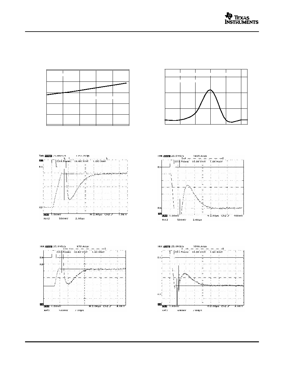
GLITCH ENERGY: 2.7-V, 1-LSB STEP, RISING EDGE
GLITCH ENERGY: 2.7-V, 1-LSB STEP, FALLING EDGE
Figure 41.
Figure 42.
GLITCH ENERGY: 2.7-V, 16-LSB STEP, RISING EDGE
GLITCH ENERGY: 2.7-V, 16-LSB STEP, FALLING EDGE
Figure 43.
Figure 44.
GLITCH ENERGY: 2.7-V, 256-LSB STEP, RISING EDGE
GLITCH ENERGY: 2.7-V, 256-LSB STEP, FALLING EDGE
Figure 45.
Figure 46.
13
www.ti.com
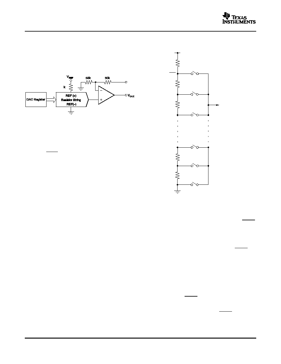
THEORY OF OPERATION
DAC SECTION
62
V
FB
GND
V
OUT
X
+
D
IN
65536
V
REF
RESISTOR STRING
To Output
Amplifier
R
R
R
R
R
VREF
V
REF
Divider
2
(2x Gain)
SERIAL INTERFACE
OUTPUT AMPLIFIER
DAC8551
SLAS429A ≠ APRIL 2005 ≠ REVISED JULY 2005
The architecture consists of a string DAC followed by
an output buffer amplifier.
Figure 47
shows a block
diagram of the DAC architecture.
Figure 47. DAC8551 Architecture
The input coding to the DAC8551 is straight binary,
so the ideal output voltage is given by:
where D
IN
= decimal equivalent of the binary code
that is loaded to the DAC register; it can range from 0
to 65535.
The resistor string section is shown in
Figure 48
. It is
simply a string of resistors, each of value R. The
Figure 48. Resistor String
code loaded into the DAC register determines at
which node on the string the voltage is tapped off to
be fed into the output amplifier by closing one of the
switches connecting the string to the amplifier. It is
monotonic because it is a string of resistors.
The DAC8551 has a 3-wire serial interface ( SYNC,
SCLK, and D
IN
), which is compatible with SPITM,
QSPITM, and MicrowireTM interface standards, as well
as most DSPs. See the Serial Write Operation timing
The output buffer amplifier is capable of generating
diagram for an example of a typical write sequence.
rail-to-rail voltages on its output, which gives an
output range of 0 V to V
DD
. It is capable of driving a
The write sequence begins by bringing the SYNC line
load of 2 k
in parallel with 1000 pF to GND. The
LOW. Data from the D
IN
line is clocked into the 24-bit
source and sink capabilities of the output amplifier
shift register on each falling edge of SCLK. The serial
can be seen in the typical curves. The slew rate is 1.8
clock frequency can be as high as 30 MHz, making
V/µs with a full-scale setting time of 8 µs with the
the DAC8551 compatible with high-speed DSPs. On
output unloaded.
the 24th falling edge of the serial clock, the last data
bit is clocked in and the programmed function is
The inverting input of the output amplifier is brought
executed (i.e., a change in DAC register contents
out to the V
FB
pin. This allows for better accuracy in
and/or a change in the mode of operation).
critical applications by tying the V
FB
point and the
amplifier output together directly at the load. Other
At this point, the SYNC line may be kept LOW or
signal conditioning circuitry may also be connected
brought HIGH. In either case, it must be brought
between these points for specific applications.
HIGH for a minimum of 33 ns before the next write
sequence so that a falling edge of SYNC can initiate
the next write sequence. As previously mentioned, it
must be brought HIGH again just before the next
write sequence.
14
www.ti.com
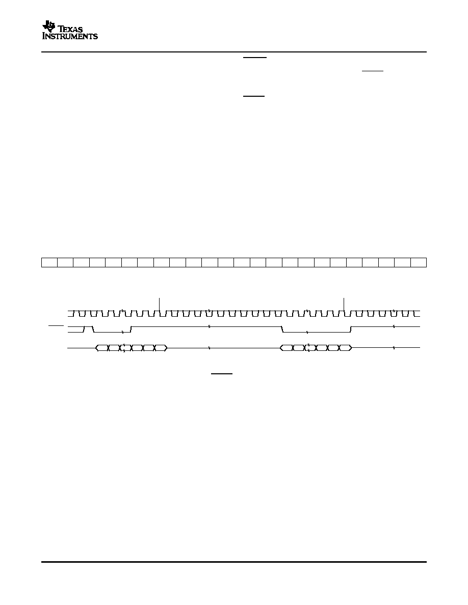
INPUT SHIFT REGISTER
SYNC INTERRUPT
POWER-ON RESET
CLK
SYNC
D
IN
Valid Write Sequence: Output Updates
on the 24th Falling Edge
24th Falling Edge
24th Falling Edge
DB23
DB80
DB23
DB80
DAC8551
SLAS429A ≠ APRIL 2005 ≠ REVISED JULY 2005
The input shift register is 24 bits wide, as shown in
In a normal write sequence, the SYNC line is kept
Figure 49
. The first six bits are don't cares. The next
LOW for at least 24 falling edges of SCLK and the
two bits (PD1 andPD0) are control bits that control
DAC is updated on the 24th falling edge. However, if
which mode of operation the part is in (normal mode
SYNC is brought HIGH before the 24th falling edge, it
or any one of three power-down modes). A more
acts as an interrupt to the write sequence. The shift
complete description of the various modes is located
register is reset, and the write sequence is seen as
in the Power-Down Modes section. The next 16 bits
invalid. Neither an update of the DAC register con-
are the data bits. These are transferred to the DAC
tents, or a change in the operating mode occurs, as
register on the 24th falling edge of SCLK.
shown in
Figure 50
.
The DAC8551 contains a power-on-reset circuit that
controls the output voltage during power up. On
power up, the DAC registers is filled with zeros and
the output voltages is 0 V; it remains there until a
valid write sequence is made to the DAC. This is
useful in applications where it is important to know
the state of the output of the DAC while it is in the
process of powering up.
DB23
DB0
X
X
X
X
X
X
PD1
PD0
D15
D14
D13
D12
D11
D10
D9
D8
D7
D6
D5
D4
D3
D2
D1
D0
Figure 49. DAC8551 Data Input Register Format
Figure 50. SYNC Interrupt Facility
15
www.ti.com
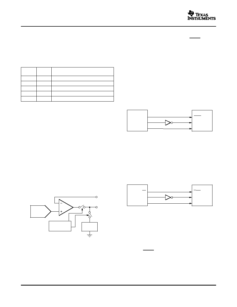
POWER-DOWN MODES
80C51/80L51
(1)
P3.3
TXD
RXD
(1)
SYNC
SCLK
D
IN
NOTE: (1) Additional pins omitted for clarity.
DAC8551
DAC8551 to Microwire Interface
SYNC
SCLK
D
IN
Microwire
TM
CS
SK
SO
DAC8551
(1)
NOTE: (1) Additional pins omitted for clarity.
DAC8551 to 68HC11 Interface
Amplifier
Power-Down
Circuitry
Resistor
Network
V
OUT
V
FB
Resistor
String DAC
MICROPROCESSOR INTERFACING
DAC8551 TO 8051 Interface
DAC8551
SLAS429A ≠ APRIL 2005 ≠ REVISED JULY 2005
The setup for the interface is as follows: TXD of the
8051 drives SCLK of the DAC8551, while RXD drives
The DAC8551 supports four separate modes of
the serial data line of the device. The SYNC signal is
operation. These modes are programmable by setting
derived from a bit-programmable pin on the port of
two bits (PD1 and PD0) in the control register.
the 8051. In this case, port line P3.3 is used. When
Table 1
shows how the state of the bits corresponds
data is to be transmitted to the DAC8551, P3.3 is
to the mode of operation of the device.
taken LOW. The 8051 transmits data in 8-bit bytes;
thus, only eight falling clock edges occur in the
Table 1. Modes of Operation for the DAC8551
transmit cycle. To load data to the DAC, P3.3 is left
PD1
PD0
OPERATING MODE
LOW after the first eight bits are transmitted, then a
(DB17)
(DB16)
second write cycle is initiated to transmit the second
0
0
Normal Operation
byte of data. P3.3 is taken HIGH following the
completion of the third write cycle. The 8051 outputs
≠
≠
Power-down modes
the serial data in a format which has the LSB first.
0
1
Output typically 1 k
to GND
The DAC8551 requires its data with the MSB as the
1
0
Output typically 100 k
to GND
first bit received. The 8051 transmit routine must
1
1
High-Z
therefore take this into account, and mirror the data
as needed.
When both bits are set to 0, the device works
normally with its typical current consumption of 200
µA at 5 V. However, for the three power-down
modes, the supply current falls to 200 nA at 5 V (50
nA at 3 V). Not only does the supply current fall, but
the output stage is also internally switched from the
output of the amplifier to a resistor network of known
values. This has the advantage that the output
impedance of the device is known while it is in
Figure 52. DAC8551 to 80C51/80L51 Interface
power-down mode. There are three different options.
The output is connected internally to GND through a
1-k
resistor,
a
100-k
resistor,
or
it
is
left
open-circuited (High-Z). The output stage is illustrated
Figure 53
shows an interface between the DAC8551
in
Figure 51
.
and any Microwire compatible device. Serial data is
All
analog
circuitry
is
shut
down
when
the
shifted out on the falling edge of the serial clock and
power-down mode is activated. However, the con-
is clocked into the DAC8551 on the rising edge of the
tents of the DAC register are unaffected when in
SK signal.
power down. The time to exit power-down is typically
2.5 µs for V
DD
= 5 V, and 5 µs for V
DD
= 3 V. See the
Typical Characteristics for more information.
Figure 53. DAC8551 to Microwire Interface
Figure 54
shows a serial interface between the
DAC8551 and the 68HC11 microcontroller. SCK of
Figure 51. Output Stage During Power Down
the 68HC11 drives the SCLK of the DAC8551, while
the MOSI output drives the serial data line of the
DAC. The SYNC signal is derived from a port line
(PC7), similar to the 8051 diagram.
See
Figure 52
for a serial interface between the
DAC8551 and a typical 8051-type microcontroller.
16
www.ti.com
68HC11
(1)
PC7
SCK
MOSI
SYNC
SCLK
D
IN
(1)
NOTE: (1) Additional pins omitted for clarity.
DAC8551
APPLICATION INFORMATION
200
m
A
)
5 V
5 k
W
+
1.2 mA
(2)
USING THE REF02 AS A POWER SUPPLY
BIPOLAR OPERATION USING THE DAC8551
V
O
+
V
REF
D
65536
R1
)
R2
R1
*
V
REF
R2
R1
REF02
Three-Wire
+5V
285
µ
A
V
OUT
= 0V to 5V
SYNC
SCLK
D
IN
+15
Serial
Interface
DAC8551
V
O
+
10
D
65536
*
5 V
(4)
LAYOUT
DAC8551
SLAS429A ≠ APRIL 2005 ≠ REVISED JULY 2005
valid on the falling edge of SCK. When data is being
transmitted to the DAC, the SYNC line is held LOW
(PC7). Serial data from the 68HC11 is transmitted in
8-bit bytes with only eight falling clock edges
occurring in the transmit cycle. (Data is transmitted
MSB first.) In order to load data to the DAC8551,
PC7 is left LOW after the first eight bits are trans-
ferred, then a second and third serial write operation
is performed to the DAC. PC7 is taken HIGH at the
Figure 54. DAC8551 to 68HC11 Interface
end of this procedure.
The 68HC11 should be configured so that its CPOL
bit is 0 and its CPHA bit is 1. This configuration
causes data appearing on the MOSI output to be
FOR THE DAC8551
The load regulation of the REF02 is typically
0.005%/mA, which results in an error of 299 µV for
Due to the extremely low supply current required by
the 1.2-mA current drawn from it. This corresponds to
the DAC8551, an alternative option is to use a REF02
a 3.9 LSB error.
+5 -V precision voltage reference to supply the re-
quired voltage to the device, as shown in
Figure 55
.
The DAC8551 has been designed for single-supply
operation, but a bipolar output range is also possible
using the circuit in
Figure 56
. The circuit shown gives
an output voltage range of
±
V
REF
. Rail-to-rail oper-
ation at the amplifier output is achievable using an
OPA703 as the output amplifier.
The output voltage for any input code can be calcu-
lated as follows:
where D represents the input code in decimal
(0≠65535).
With V
REF
= 5 V, R1 = R2 = 10 k
.
Figure 55. REF02 as a Power Supply to the
DAC8551
This is especially useful if the power supply is quite
This is an output voltage range of
±
5 V with 0000
H
noisy or if the system supply voltages are at some
corresponding to a ≠5 V output and FFFF
H
corre-
value other than 5 V. The REF02 outputs a steady
sponding to a 5 V output. Similarly, using V
REF
= 2.5
supply voltage for the DAC8551. If the REF02 is
V, a
±
2.5-V output voltage range can be achieved.
used, the current it needs to supply to the DAC8551
is 200 µA. This is with no load on the output of the
DAC. When a DAC output is loaded, the REF02 also
needs to supply the current to the load. The total
A precision analog component requires careful layout,
typical current required (with a 5-k
load on the DAC
adequate bypassing, and clean, well-regulated power
output) is:
supplies.
The DAC8551 offers single-supply operation, and it
often is used in close proximity with digital logic,
17
www.ti.com
DAC8551
V
REF
V
OUT
V
FB
R
1
10k
R
2
10k
V
REF
10
µ
F
0.1
µ
F
≠5V
±
5V
+5V
OPA703
Three-Wire
Serial Interface
DAC8551
SLAS429A ≠ APRIL 2005 ≠ REVISED JULY 2005
microcontrollers, microprocessors, and digital signal
The power applied to V
DD
should be well regulated
processors. The more digital logic present in the
and low noise. Switching power supplies and DC/DC
design and the higher the switching speed, the more
converters often have high-frequency glitches or
difficult it is to keep digital noise from appearing at
spikes riding on the output voltage. In addition, digital
the output.
components can create similar high-frequency spikes
as their internal logic switches states. This noise can
Due to the single ground pin of the DAC8551, all
easily couple into the DAC output voltage through
return currents, including digital and analog return
various paths between the power connections and
currents for the DAC, must flow through a single
analog output.
point. Ideally, GND would be connected directly to an
analog ground plane. This plane would be separate
As with the GND connection, V
DD
should be connec-
from
the
ground
connection
for
the
digital
ted to a 5-V power-supply plane or trace that is
components
until
they
were
connected
at
the
separate from the connection for digital logic until
power-entry point of the system.
they are connected at the power-entry point. In
addition, a 1-µF to 10-µF capacitor and 0.1-µF
bypass capacitor are strongly recommended. In some
situations, additional bypassing may be required,
such as a 100-µF electrolytic capacitor or even a Pi
filter made up of inductors and capacitors ≠ all
designed to essentially low-pass filter the 5-V supply,
removing the high-frequency noise.
Figure 56. Bipolar Output Range
18
PACKAGING INFORMATION
Orderable Device
Status
(1)
Package
Type
Package
Drawing
Pins Package
Qty
Eco Plan
(2)
Lead/Ball Finish
MSL Peak Temp
(3)
DAC8551IDGK
ACTIVE
MSOP
DGK
8
80
Green (RoHS &
no Sb/Br)
CU
Level-1-260C-UNLIM
DAC8551IDGKR
ACTIVE
MSOP
DGK
8
2500 Green (RoHS &
no Sb/Br)
CU
Level-1-260C-UNLIM
DAC8551IDGKRG4
ACTIVE
MSOP
DGK
8
2500 Green (RoHS &
no Sb/Br)
CU
Level-1-260C-UNLIM
DAC8551IDGKT
ACTIVE
MSOP
DGK
8
250
Green (RoHS &
no Sb/Br)
CU
Level-1-260C-UNLIM
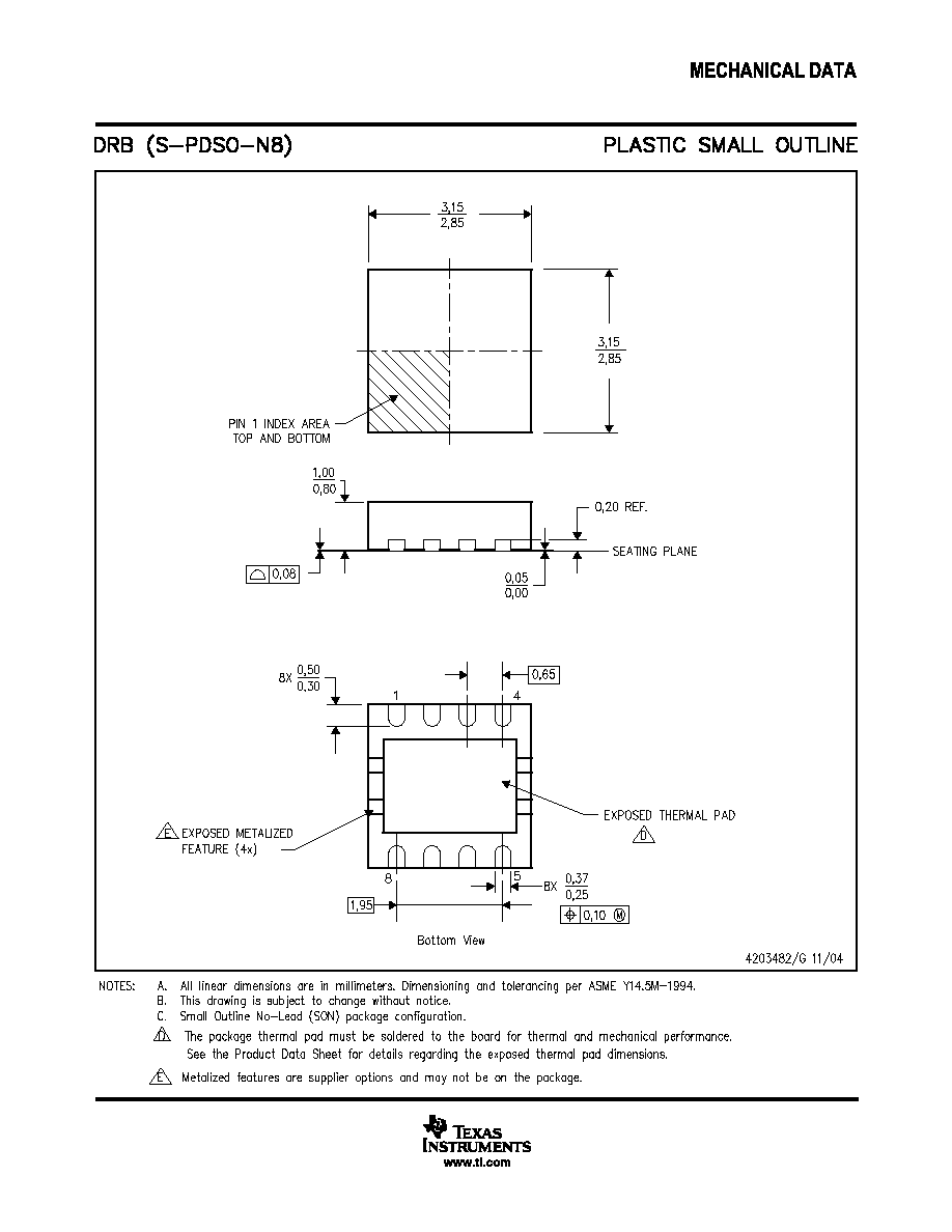
DAC8551IDRBR
PREVIEW
SON
DRB
8
3000
TBD
Call TI
Call TI
DAC8551IDRBT
PREVIEW
SON
DRB
8
250
TBD
Call TI
Call TI
(1)
The marketing status values are defined as follows:
ACTIVE: Product device recommended for new designs.
LIFEBUY: TI has announced that the device will be discontinued, and a lifetime-buy period is in effect.
NRND: Not recommended for new designs. Device is in production to support existing customers, but TI does not recommend using this part in
a new design.
PREVIEW: Device has been announced but is not in production. Samples may or may not be available.
OBSOLETE: TI has discontinued the production of the device.
(2)
Eco
Plan
-
The
planned
eco-friendly
classification:
Pb-Free
(RoHS)
or
Green
(RoHS
&
no
Sb/Br)
-
please
check
http://www.ti.com/productcontent
for the latest availability information and additional product content details.
TBD: The Pb-Free/Green conversion plan has not been defined.
Pb-Free (RoHS): TI's terms "Lead-Free" or "Pb-Free" mean semiconductor products that are compatible with the current RoHS requirements
for all 6 substances, including the requirement that lead not exceed 0.1% by weight in homogeneous materials. Where designed to be soldered
at high temperatures, TI Pb-Free products are suitable for use in specified lead-free processes.
Green (RoHS & no Sb/Br): TI defines "Green" to mean Pb-Free (RoHS compatible), and free of Bromine (Br) and Antimony (Sb) based flame
retardants (Br or Sb do not exceed 0.1% by weight in homogeneous material)
(3)
MSL, Peak Temp. -- The Moisture Sensitivity Level rating according to the JEDEC industry standard classifications, and peak solder
temperature.
Important Information and Disclaimer:The information provided on this page represents TI's knowledge and belief as of the date that it is
provided. TI bases its knowledge and belief on information provided by third parties, and makes no representation or warranty as to the
accuracy of such information. Efforts are underway to better integrate information from third parties. TI has taken and continues to take
reasonable steps to provide representative and accurate information but may not have conducted destructive testing or chemical analysis on
incoming materials and chemicals. TI and TI suppliers consider certain information to be proprietary, and thus CAS numbers and other limited
information may not be available for release.
In no event shall TI's liability arising out of such information exceed the total purchase price of the TI part(s) at issue in this document sold by TI
to Customer on an annual basis.
PACKAGE OPTION ADDENDUM
www.ti.com
27-Sep-2005
Addendum-Page 1

IMPORTANT NOTICE
Texas Instruments Incorporated and its subsidiaries (TI) reserve the right to make corrections, modifications,
enhancements, improvements, and other changes to its products and services at any time and to discontinue
any product or service without notice. Customers should obtain the latest relevant information before placing
orders and should verify that such information is current and complete. All products are sold subject to TI's terms
and conditions of sale supplied at the time of order acknowledgment.
TI warrants performance of its hardware products to the specifications applicable at the time of sale in
accordance with TI's standard warranty. Testing and other quality control techniques are used to the extent TI
deems necessary to support this warranty. Except where mandated by government requirements, testing of all
parameters of each product is not necessarily performed.
TI assumes no liability for applications assistance or customer product design. Customers are responsible for
their products and applications using TI components. To minimize the risks associated with customer products
and applications, customers should provide adequate design and operating safeguards.
TI does not warrant or represent that any license, either express or implied, is granted under any TI patent right,
copyright, mask work right, or other TI intellectual property right relating to any combination, machine, or process
in which TI products or services are used. Information published by TI regarding third-party products or services
does not constitute a license from TI to use such products or services or a warranty or endorsement thereof.
Use of such information may require a license from a third party under the patents or other intellectual property
of the third party, or a license from TI under the patents or other intellectual property of TI.
Reproduction of information in TI data books or data sheets is permissible only if reproduction is without
alteration and is accompanied by all associated warranties, conditions, limitations, and notices. Reproduction
of this information with alteration is an unfair and deceptive business practice. TI is not responsible or liable for
such altered documentation.
Resale of TI products or services with statements different from or beyond the parameters stated by TI for that
product or service voids all express and any implied warranties for the associated TI product or service and
is an unfair and deceptive business practice. TI is not responsible or liable for any such statements.
Following are URLs where you can obtain information on other Texas Instruments products and application
solutions:
Products
Applications
Amplifiers
amplifier.ti.com
Audio
www.ti.com/audio
Data Converters
dataconverter.ti.com
Automotive
www.ti.com/automotive
DSP
dsp.ti.com
Broadband
www.ti.com/broadband
Interface
interface.ti.com
Digital Control
www.ti.com/digitalcontrol
Logic
logic.ti.com
Military
www.ti.com/military
Power Mgmt
power.ti.com
Optical Networking
www.ti.com/opticalnetwork
Microcontrollers
microcontroller.ti.com
Security
www.ti.com/security
Telephony
www.ti.com/telephony
Video & Imaging
www.ti.com/video
Wireless
www.ti.com/wireless
Mailing Address:
Texas Instruments
Post Office Box 655303 Dallas, Texas 75265
Copyright
2005, Texas Instruments Incorporated