Document Outline
- FEATURES
- APPLICATIONS
- DESCRIPTION
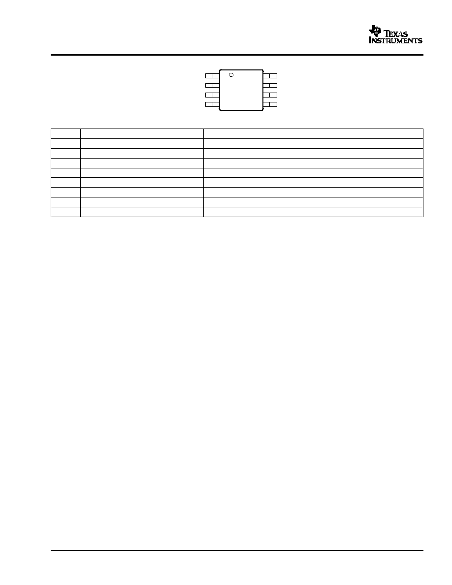
- PIN CONFIGURATIONS
- PIN DESCRIPTION
- PACKAGE/ORDERING INFORMATION
- ABSOLUTE MAXIMUM RATINGS
- ELECTRICAL CHARACTERISTICS
- TIMING CHARACTERISTICS
- TYPICAL CHARACTERISTICS
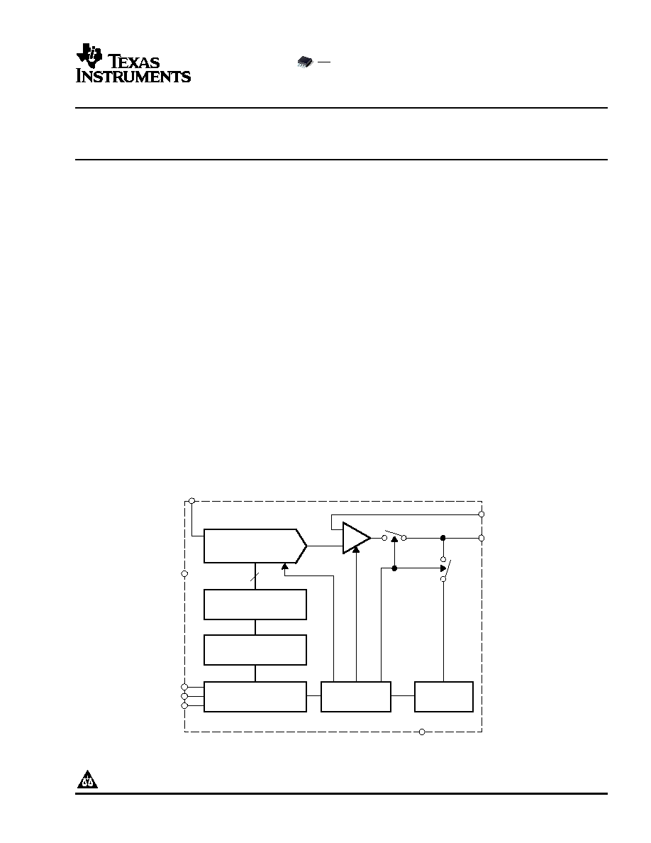
- THEORY OF OPERATION
- D/A SECTION
- RESISTOR STRING
- Output Amplifier
- I2C Interface
- Master Writing to a Slave Receiver (Standard/Fast Modes)
- Master Reading From a Slave Transmitter (Standard/Fast Modes)
- Master Writing to a Slave Receiver (High-Speed Mode)
- Master Receiver Reading From a Slave Transmitter (High-Speed Mode)
- DAC8571 Update Sequence
- DAC8571 Address Byte
- Control Byte
- Most Significant Byte
- Least Significant Byte
- Data Transmit and Read-Back
- EXAMPLES (A0 TIED TO GND, VDD = 5 V)
- Power-On Reset
- Power-Down Modes
- CURRENT CONSUMPTION
- DRIVING RESISTIVE AND CAPACITIVE LOADS
- AC PERFORMANCE
- OUTPUT VOLTAGE STABILITY
- SETTLING TIME AND OUTPUT GLITCH PERFORMANCE
- USING REF02 AS A POWER SUPPLY FOR DAC8571
- LAYOUT
3 mm x 5 mm
www.ti.com
_
+
16 Bit DAC
DAC Register
I
2
C Block
Power Down
Control Logic
Resistor
Network
16
Ref +
V
REF
V
DD
SDA
SCL
A0
GND
V
(SENSE)
V
OUT
Temporary Register
DAC8571
SLAS373A � DECEMBER 2002 � REVISED JULY 2003
16-BIT, LOW POWER, VOLTAGE OUTPUT, I
2
C INTERFACE DIGITAL-TO-ANALOG
CONVERTER
FEATURES
DESCRIPTION
�
Micropower Operation: 160 �A @ 5 V
The DAC8571 is a small low-power, 16-bit voltage
�
Power-On Reset to Zero
output DAC with an I
2
C compatible two-wire serial
interface. Its on-chip precision output amplifier allows
�
Single Supply: +2.7 V to +5.5 V
rail-to-rail
output
swing
and
settles
within
10
�
16-Bit Monotonic
microseconds. The DAC8571 architecture is 16-bit
�
Settling Time: 10 �s to
�0.003% FSR
monotonic, and factory trimming typically achieves
�4
�
I
2
CTM Interface With High-Speed Mode
mV absolute accuracy at all codes. The DAC8571
requires an external reference voltage to set its output
�
Supports Data Receive and Transmit
voltage range.
�
On-Chip Rail-to-Rail Output Buffer
�
Double-Buffered Input Register
The low power consumption and small size of this part
make it ideally suited to portable battery operated
�
Supports Synchronous Multichannel Update
equipment. The power consumption is typically 800 �W
�
Offset Error:
�1 mV max at 25�C
at V
DD
= 5 V reducing to 1 �W in power-down mode.
�
Full-Scale Error:
�3 mV max at 25�C
The DAC8571 incorporates a 2-wire I
2
C interface.
�
Small 8 Lead MSOP Package
Standard, fast, and high-speed modes of I
2
C operation
are all supported up to 3.4 MHz serial clock speeds.
APPLICATIONS
Multichannel
synchronous
data
update
and
�
Process Control
power-down operations are supported through the I
2
C
bus. DAC8571 is also capable of transmitting the con-
�
Data Acquisition Systems
tents of its serial shift register, a key feature for I
2
C
�
Closed-Loop Servo Control
system verification.
�
PC Peripherals
The DAC8571 is available in an 8-lead MSOP package
�
Portable Instrumentation
and is specified over -40
�C to 105�C.
I2C is a trademark of Philips Corporation.
Please be aware that an important notice concerning availability, standard warranty, and use in critical applications of Texas Instruments
semiconductor products and disclaimers thereto appears at the end of this data sheet.
PRODUCTION DATA information is current as of publication date.
Copyright � 2002 � 2003, Texas Instruments Incorporated
Products conform to specifications per the terms of Texas Instruments
standard warranty. Production processing does not necessarily in-
clude testing of all parameters.
www.ti.com
GND
SDA
SCL
A0
8
7
6
5
1
2
3
4
V
DD
V
REF
V
(SENSE)
V
OUT
DAC8571
SLAS373A � DECEMBER 2002 � REVISED JULY 2003
PIN CONFIGURATIONS
PIN DESCRIPTION
Pin
Name
Function
1
V
DD
Analog voltage supply input
2
V
REF
Positive reference voltage input
3
V
(SENSE)
Analog output sense
4
V
OUT
Analog output voltage from DAC
5
A0
Device address select
6
SCL
Serial clock input
7
SDA
Serial data input/output
8
GND
Ground reference point for all circuitry on the part
2
www.ti.com
DAC8571
SLAS373A � DECEMBER 2002 � REVISED JULY 2003
These devices have limited built-in ESD protection. The leads should be shorted together or the device placed in conductive foam
during storage or handling to prevent electrostatic damage to the MOS gates.
PACKAGE/ORDERING INFORMATION
Product
Package
Package Desig-
Specified Temperature
Package
Ordering Number
Transport Me-
nator
Range
Marking
dia, Quantity
DAC8571
8-MSOP
DGK
-40
�C to +105�C
D871
DAC8571IDGK
Tube, 80
DAC8571IDGKR
Tape & Reel,
2500
ABSOLUTE MAXIMUM RATINGS (1)
DAC8571
V
DD
to GND
-0.3 V to +6 V
Digital input voltage to GND
-0.3V to V
DD
+ 0.3V
V
OUT
to GND
-0.3V to +V
DD
+ 0.3V
Operating temperature range
-40
�C to + 105�C
Storage temperature range
-65
�C to +150�C
Junction temperature range (T
J
max)
+ 150
�C
JA
Thermal impedance
260
�C/W
JC
Thermal impedance
44
�C/W
Lead temperature, soldering
Vapor phase
215
�C
(60s)
Infrared (15s)
220
�C
(1)
Stresses above those listed under "Absolute Maximum Ratings" may cause permanent damage to the device. Exposure to absolute
maximum conditions for extended periods may affect device reliability.
ELECTRICAL CHARACTERISTICS
V
DD
= +2.7 V to +5.5 V; R
L
= 2 k
to GND; C
L
= 200 pF to GND; low power mode; all specifications -40
�C to 105�C (unless
otherwise noted)
DAC8571
PARAMETER
CONDITIONS
MIN
TYP
MAX
UNITS
STATIC PERFORMANCE (1)
Resolution
16
Bits
Relative accuracy
�0.098
% of FSR
Differential nonlinearity
Monotonic by design
�0.25
�1
LSB
Offset error
Measured at code 485, 25
�C
0.3
�1.0
mV
Measured at code 485, -40
�C...105�C
1.0
�5.0
Full-scale error
Measured at code 64714, 25
�C
0.5
�3.0
mV
Measured at code 64714, -40
�C...105�C
1.0
�5.0
Gain error
Measured at code 64714, 25
�C
1.0
�3.0
mV
Measured at code 64714, -40
�C...105�C
2.0
�5.0
Zero code error drift
All zeroes loaded to DAC register
-20
�V/
�C
Gain temperature coefficient
-5
ppm of FSR/
�C
Absolute accuracy
All codes from code 485 to code 64714, 25
�C
�2.5
mV
All codes from code 485 to code 64714,
�3.5
-40
�C...105�C
(1)
Linearity calculated using a reduced code range of 485 to 64714. Output unloaded.
3
www.ti.com
DAC8571
SLAS373A � DECEMBER 2002 � REVISED JULY 2003
ELECTRICAL CHARACTERISTICS (continued)
V
DD
= +2.7 V to +5.5 V; R
L
= 2 k
to GND; C
L
= 200 pF to GND; low power mode; all specifications -40
�C to 105�C (unless
otherwise noted)
DAC8571
PARAMETER
CONDITIONS
MIN
TYP
MAX
UNITS
OUTPUT CHARACTERISTICS (2)
Output voltage range
0
V
REF
V
Output voltage settling time (full
R
L
= 2 k
; C
L
< 200 pF, fast settling
8
10
�s
scale)
R
L
= 2 k
; C
L
= 500 pF, fast settling
12
�s
R
L
= 2 k
; C
L
< 200 pF, low power
13
15
�s
Slew rate
R
L
= 2 k
; C
L
< 200 pF, fast settling
1
V/�s
R
L
= 2 k
; C
L
< 200 pF, low power
0.5
Capacitive load stability
R
L
=
470
pF
R
L
= 2 k
1000
pF
Digital-to-analog glitch impulse
20
nV-s
Digital feedthrough
0.5
nV-s
DC output impedance
1
Short circuit current
V
DD
= +5 V
50
mA
V
DD
= +3 V
20
mA
Power-up time
Coming out of power-down mode, V
DD
= +5 V
2.5
�s
Coming out of power-down mode, V
DD
= +3 V
5
�s
PSRR
0.75
mV/V
REFERENCE INPUT
V
REFH
input range
0
V
DD
V
Reference input impedance
140
k
LOGIC INPUTS (3)
Input current
�1
�A
V
IN_L
, Input low voltage
V
DD
= 2.7-5.5 V
0.3V
DD
V
V
IN_H0
, Input high voltage
V
DD
= 2.7-5.5 V
0.7V
DD
V
Pin capacitance
3
pF
POWER REQUIREMENTS
V
DD
2.7
5.5
V
I
DD
(normal operation)
DAC active, I
ref
included
V
DD
= +4.5 V to +5.5 V
V
IH
= V
DD
, V
IL
= GND, fast settling
250
400
�A
V
IH
= V
DD
, V
IL
= GND, low power
160
225
V
DD
= +2.7 V to +3.6 V
V
IH
= V
DD
, V
IL
= GND, fast settling
240
380
�A
V
IH
= V
DD
, V
IL
= GND, low power
140
200
I
DD
(all power-down modes)
DAC active, I
ref
included
V
DD
= +4.5 V to +5.5 V
V
IH
= V
DD
and V
IL
= GND
0.2
1
�A
V
DD
= +2.7 V to +3.6 V
V
IH
= V
DD
and V
IL
= GND
0.05
1
�A
POWER EFFICIENCY
I
OUT
/I
DD
I
L
= 2 mA, V
DD
= +5 V
93%
(2)
Assured by design and characterization, not production tested.
(3)
Assured by design and characterization, not production tested.
4

www.ti.com
DAC8571
SLAS373A � DECEMBER 2002 � REVISED JULY 2003
TIMING CHARACTERISTICS
V
DD
= +2.7 V to +5.5 V; R
L
= 2 k
to GND; all specifications -40�C to 105�C (unless otherwise noted)
SYMBOL
PARAMETER
TEST CONDITIONS
MIN
TYP
MAX
UNITS
Standard mode
100
kHz
Fast mode
400
kHz
t
SCL
SCL clock frequency
High-speed mode, C
B
- 100pF max
3.4
MHz
High-speed mode, C
B
- 400pF max
1.7
MHz
Standard mode
4.7
�s
Bus free time between a STOP and
t
BUF
START condition
Fast mode
1.3
�s
Standard mode
4.0
\�s
Hold time (repeated) START con-
t
HO
; t
STA
Fast mode
600
ns
dition
High-speed mode
160
ns
Standard mode
4.7
�s
t
LOW
LOW period of the SCL clock
Fast mode
1.3
�s
Standard mode
4.0
�s
Fast mode
600
ns
t
HIGH
HIGH period of the SCL clock
High-speed mode, C
B
- 100pF max
60
ns
High-speed mode, C
B
- 400pF max
120
ns
Standard mode
4.7
�s
Setup time for a repeated START
t
SU
; t
STA
Fast mode
600
ns
condition
High-speed mode
160
ns
Standard mode
250
ns
t
SU
; t
DAT
Data setup time
Fast mode
100
ns
High-speed mode
10
ns
Standard mode
0
0.9
�s
Fast mode
0
0.9
�s
t
HD
; t
DAT
Data hold time
High-speed mode, C
B
- 100pF max
0
70
ns
High-speed mode, C
B
- 400pF max
0
150
ns
Standard mode
20
� 0.1C
B
1000
ns
Fast mode
20
� 0.1C
B
300
ns
t
RCL
Rise time of SCL signal
High-speed mode, C
B
- 100pF max
10
40
ns
High-speed mode, C
B
- 400pF max
20
80
ns
Standard mode
20
� 0.1C
B
1000
ns
Rise time of SCL signal after a
Fast mode
20
� 0.1C
B
300
ns
t
RCL1
repeated START condition, and
High-speed mode, C
B
- 100pF max
10
80
ns
after an acknowledge BIT
High-speed mode, C
B
- 400pF max
20
1600
ns
Standard mode
20
� 0.1C
B
300
ns
Fast mode
20
� 0.1C
B
300
ns
t
FCL
Fall time of SCL signal
High-speed mode, C
B
- 100pF max
10
40
ns
High-speed mode, C
B
- 400pF max
20
80
ns
Standard mode
20
� 0.1C
B
1000
ns
Fast mode
20
� 0.1C
B
300
ns
t
RCA
Rise time of SDA signal
High-speed mode, C
B
- 100pF max
10
80
ns
High-speed mode, C
B
- 400pF max
20
160
ns
Standard mode
20
� 0.1C
B
300
ns
Fast mode
20
� 0.1C
B
300
ns
t
FDA
Fall time of SDA signal
High-speed mode, C
B
- 100pF max
10
80
ns
High-speed mode, C
B
- 400pF max
20
160
ns
5

www.ti.com
DAC8571
SLAS373A � DECEMBER 2002 � REVISED JULY 2003
TIMING CHARACTERISTICS (continued)
V
DD
= +2.7 V to +5.5 V; R
L
= 2 k
to GND; all specifications -40�C to 105�C (unless otherwise noted)
SYMBOL
PARAMETER
TEST CONDITIONS
MIN
TYP
MAX
UNITS
Standard mode
4.0
�s
t
SU
; t
STO
Setup time for STOP condition
Fast mode
600
ns
High-speed mode
160
ns
C
B
Capacitive load for SDA and SCL
400
pF
Fast mode
50
ns
t
SP
Pulse width of spike suppressed
High-speed mode
10
ns
Standard mode
Noise margin at the HIGH level for
V
NH
each connected device (including
Fast mode
0.2V
DO
V
hysteresis)
High-speed mode
Standard mode
Noise margin at the LOW level for
V
NL
each connected device (including
Fast mode
0.1V
DO
V
hysteresis)
High-speed mode
6

www.ti.com
1
0.8
0.6
0.4
0.2
0
- 0.2
- 0.4
- 0.6
- 0.8
- 1
0
10000 20000
30000
40000
50000 60000
DLE
-
LSB
Digital Input Code
-64
-48
-32
-16
0
16
32
48
64
0
10000
20000
30000
40000
50000
60000
Digital Input Code
Linearity Erro
r - LSB
T
A
� Free�Air Temperature �
�
C
�3
�2
�1
0
1
2
3
�40
�20
0
20
40
60
80
100
Error � mV
Zero�Scale
Full�Scale
Gain
V
DD
= 5 V
�3
�2
�1
0
1
2
3
�40
�20
0
20
40
60
80
100
T
A
� Free�Air Temperature �
�
C
Error � mV
Zero�Scale
Full�Scale
Gain
V
DD
= 3 V
- 64
- 48
- 32
- 16
0
16
32
48
64
- 40
0
40
80
110
T
A
- Free-Air Temperature -
�
C
Linearity Error
-
LSB
MAX Error
MIN Error
- 1
- 0.8
- 0.6
- 0.4
- 0.2
0
0.2
0.4
0.6
0.8
1
- 40
0
40
80
110
MAX Error
MIN Error
T
A
- Free-Air Temperature -
�
C
Differential Linearity Error
-
LSB
DAC8571
SLAS373A � DECEMBER 2002 � REVISED JULY 2003
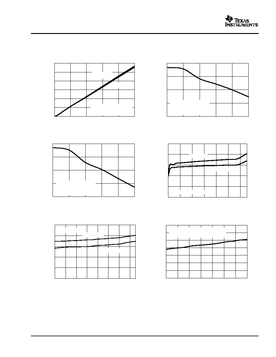
TYPICAL CHARACTERISTICS
At T
A
= +25
�C, unless otherwise noted.
DIFFERENTIAL LINEARITY ERROR vs DIGITAL INPUT
LINEARITY ERROR vs DIGITAL INPUT CODE
CODE
Figure 1.
Figure 2.
ERROR vs TEMPERATURE
ERROR vs TEMPERATURE
Figure 3.
Figure 4.
LINEARITY ERROR
DIFFERENTIAL LINEARITY ERROR
vs
vs
TEMPERATURE
TEMPERATURE
Figure 5.
Figure 6.
7
www.ti.com
0
0.025
0.05
0.075
0.1
0.125
0.15
0
1
2
3
4
5
I
SINK
- Sink Current - mA
V
OUT
- Output
V
oltage - V
V
REF
= V
DD
- 10 mV
DAC Loaded With 0000
H
V
DD
= 2.7 V
V
DD
= 5 V
4.8
4.85
4.9
4.95
5
0
1
2
3
4
5
I
SOURCE
- Source Current - mA
V
OUT
- Output
V
oltage - V
V
REF
= V
DD
- 10 mV
DAC Loaded With FFFF
H
V
DD
= 5 V
2.5
2.55
2.6
2.65
2.7
0
1
2
3
4
5
I
SOURCE
- Source Current - mA
V
OUT
- Output
V
oltage - V
V
REF
= V
DD
- 10 mV
DAC Loaded With FFFF
H
V
DD
= 2.7 V
0
50
100
150
200
250
0
10000
20000
30000
40000
50000
60000
Digital Input Code
I
DD
- Supply Curr
ent -
�
A
V
DD
= 5 V
V
DD
= 3.6 V
Reference Current Included
T
A
� Free�Air Temperature �
�
C
0
50
100
150
200
250
�40
�20
0
20
40
60
80
100
I
D
D
� Supply Current �
�
A
V
DD
= 3.6 V
V
DD
= 5.5 V
I
REF
Included
0
20
40
60
80
100
120
140
2.7
3.1
3.5
3.9
4.3
4.7
5.1
5.5
V
DD
- Supply Voltage - V
I
DD
- Supply Curr
ent -
�
A
V
REF
= V
DD
, I
DD
Measured at Power-Up,
Reference Current Included, No Load
DAC8571
SLAS373A � DECEMBER 2002 � REVISED JULY 2003
TYPICAL CHARACTERISTICS (continued)
At T
A
= +25
�C, unless otherwise noted.
SINK CURRENT AT NEGATIVE RAIL
SOURCE CURRENT AT POSITIVE RAIL
Figure 7.
Figure 8.
SOURCE CURRENT AT POSITIVE RAIL
SUPPLY CURRENT vs DIGITAL INPUT CODE
Figure 9.
Figure 10.
SUPPLY CURRENT vs TEMPERATURE
SUPPLY CURRENT vs SUPPLY VOLTAGE
Figure 11.
Figure 12.
8

www.ti.com
0
500
1000
1500
2000
2500
0
40
80
120
160
200
240
280
I
DD
- Supply Current -
�
A
f - F
requency
I
REF
Included
V
DD
= 2.7 V
V
DD
= 5.5 V
0
0.1
0.2
0.3
0.4
0.5
0.6
0.7
0.8
0.9
1
0
1
2
3
4
5
Logic Input Voltage - V
I
DD
- Supply Curr
ent - mA
T
A
= 25
�
C,
A0 Input (All Other Inputs = GND)
Reference Current Included
V
DD
= V
REF
= 2.7 V
V
DD
= V
REF
= 5.5 V
t - Time - 5
�
s/div
-0.5
0
0.5
1
1.5
2
2.5
3
3.5
4
4.5
5
5.5
V
OUT
- Output
V
oltage - V
2.3
2.35
2.4
2.45
2.5
0
5
10
15
20
25
30
V O
(V
, 50 mV/div)
t - Time -
�
S
V
ref
= V
DD
- 50 mV
Code 7FFFh to 8000h
(Glitch Occurs Every N x 4096
Code Boundary)
0
1
2
3
4
5
6
t � Time � 12
�
s/div, Fast�Settling Mode
V
O
U
T
� Output V
oltage � V
V
DD
= V
REF
= 5 V
Output
Loaded With
2 k
and
200 pF to
GND
-0.005
-0.004
-0.003
-0.002
-0.001
0
0.001
0.002
0.003
0.004
0.005
0
10000 20000 30000 40000 50000 60000
Digital Input Code
T
otal Unadjusted Error
- V
V
DD
= 5 V
DAC8571
SLAS373A � DECEMBER 2002 � REVISED JULY 2003
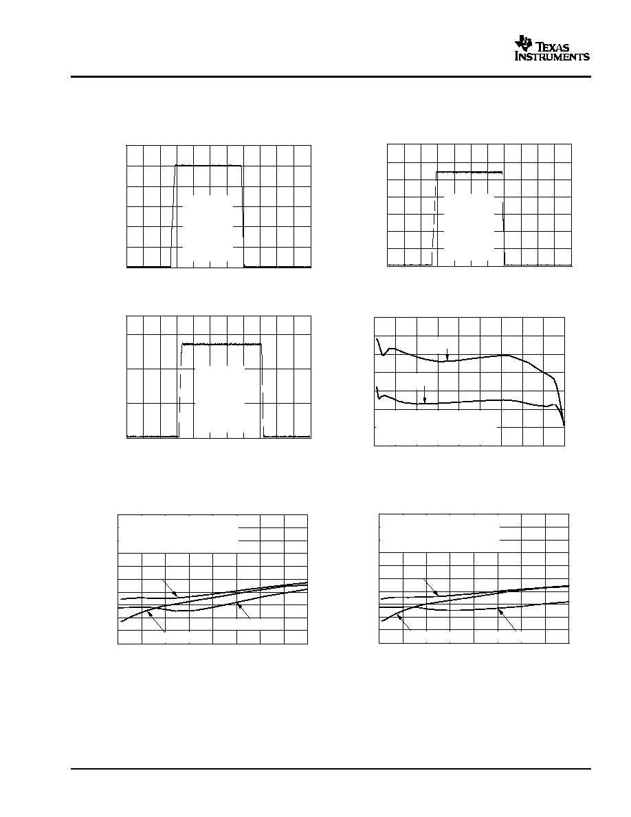
TYPICAL CHARACTERISTICS (continued)
At T
A
= +25
�C, unless otherwise noted.
SUPPLY CURRENT vs LOGIC INPUT VOLTAGE
HISTOGRAM OF CURRENT CONSUMPTION
Figure 13.
Figure 14.
EXITING POWER-DOWN MODE
OUTPUT GLITCH (Mid-Scale)
Figure 15.
Figure 16.
ABSOLUTE ERROR
FULL-SCALE SETTLING TIME (Large Signal)
Figure 17.
Figure 18.
9
www.ti.com
0.0
0.5
1.0
1.5
2.0
2.5
3.0
3.5
t � Time � 12
�
s/div, Fast�Settling Mode
V
O
U
T
� Output V
oltage � V
V
DD
= V
REF
= 2.7 V
Output
Loaded With
2 k
and
200 pF to
GND
0.0
0.5
1.0
1.5
2.0
2.5
3.0
t � Time � 12
�
s/div, Fast�Settling Mode
V
O
U
T
� Output V
oltage � V
V
DD
= V
REF
= 5 V
Output
Loaded With
2 k
and
200 pF to
GND
0.00
0.50
1.00
1.50
t � Time � 12
�
s/div, Fast�Settling Mode
V
O
U
T
� Output V
oltage � V
V
DD
= V
REF
= 2.7 V
Output
Loaded With
2 k
and
200 pF to
GND
V
DD
= 5V
V
DD
= 2.7V
V
DD
= V
REF
-1dB FSR Digital Input, F
S
= 52ksps
Measurement Bandwidth = 20kHz
SIGNAL-T O-NOISE RATIO vs OUTPUT FREQUENCY
98
96
94
92
90
88
86
84
SNR (dB)
0
500
1k
1.5k
2k
2.5k
3k
3.5k
4k
4.5k
Output Frequency (Hz), Fast-Settling Mode
V
DD
= V
REF
= 2.7V
F
S
= 52ksps, - 1dB FSR Digital Input
Measurement Bandwidth = 20kHz
THD
3rd Harmonic
0
- 10
- 20
- 30
- 40
- 50
- 60
- 70
- 80
- 90
- 100
THD (dB)
0
500
1k
1.5k
2k
2.5k
3k
3.5k
4k
Output Frequency (Hz), Fast - Settling Mode
2nd Harmonic
V
DD
= V
REF
= 5V
F
S
= 52ksps, - 1dB FSR Digital Input
Measurement Bandwidth = 20kHz
THD
2nd Harmonic
3rd Harmonic
OUTPUT FREQUENCY
0
- 10
- 20
- 30
- 40
- 50
- 60
- 70
- 80
- 90
- 100
THD (dB)
0
500
1k
1.5k
2k
2.5k
3k
3.5k
4k
Output Frequency (Hz), Fast-Settling Mode
DAC8571
SLAS373A � DECEMBER 2002 � REVISED JULY 2003
TYPICAL CHARACTERISTICS (continued)
At T
A
= +25
�C, unless otherwise noted.
HALF-SCALE SETTLING TIME (Large Signal)
FULL-SCALE SETTLING TIME (Large Signal)
Figure 19.
Figure 20.
HALF-SCALE SETTLING TIME
SIGNAL-TO-NOISE RATIO vs OUTPUT FREQUENCY
Figure 21.
Figure 22.
TOTAL HARMONIC DISTORTION vs OUTPUT FRE-
TOTAL HARMONIC DISTORTION vs OUTPUT FRE-
QUENCY
QUENCY
Figure 23.
Figure 24.
10

www.ti.com
Time (2
�
s/div)
Small-Signal Settling
Time
5mV/div
Output V
oltage
Trigger
Signal
Time (2
�
s/div)
Small-Signal Settling
Time
5mV/div
Output V
oltage
Trigger
Signal
DAC8571
SLAS373A � DECEMBER 2002 � REVISED JULY 2003
TYPICAL CHARACTERISTICS (continued)
At T
A
= +25
�C, unless otherwise noted.
FULL-SCALE SETTLING TIME
FULL-SCALE SETTLING TIME
(Small-Signal-Positive Going Step)
(Small-Signal-Negative Going Step)
Figure 25.
Figure 26.
11
www.ti.com
_
+
Resistor
String
Ref+
Ref-
Reference Voltage
GND
DAC Register
V
(SENSE)
V
OUT
V
OUT
+
V
REF
D
65536
(1)
R
R
R
R
V
REF
GND
To Output
Amplifier
DAC8571
SLAS373A � DECEMBER 2002 � REVISED JULY 2003
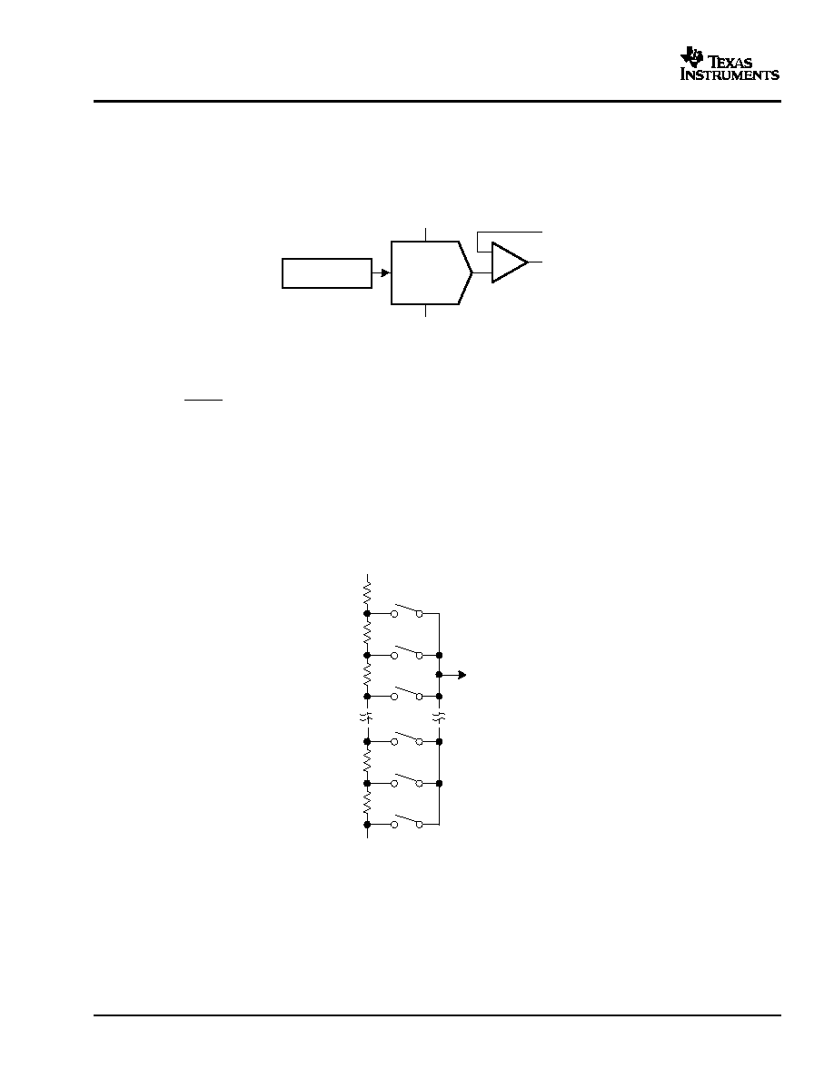
THEORY OF OPERATION
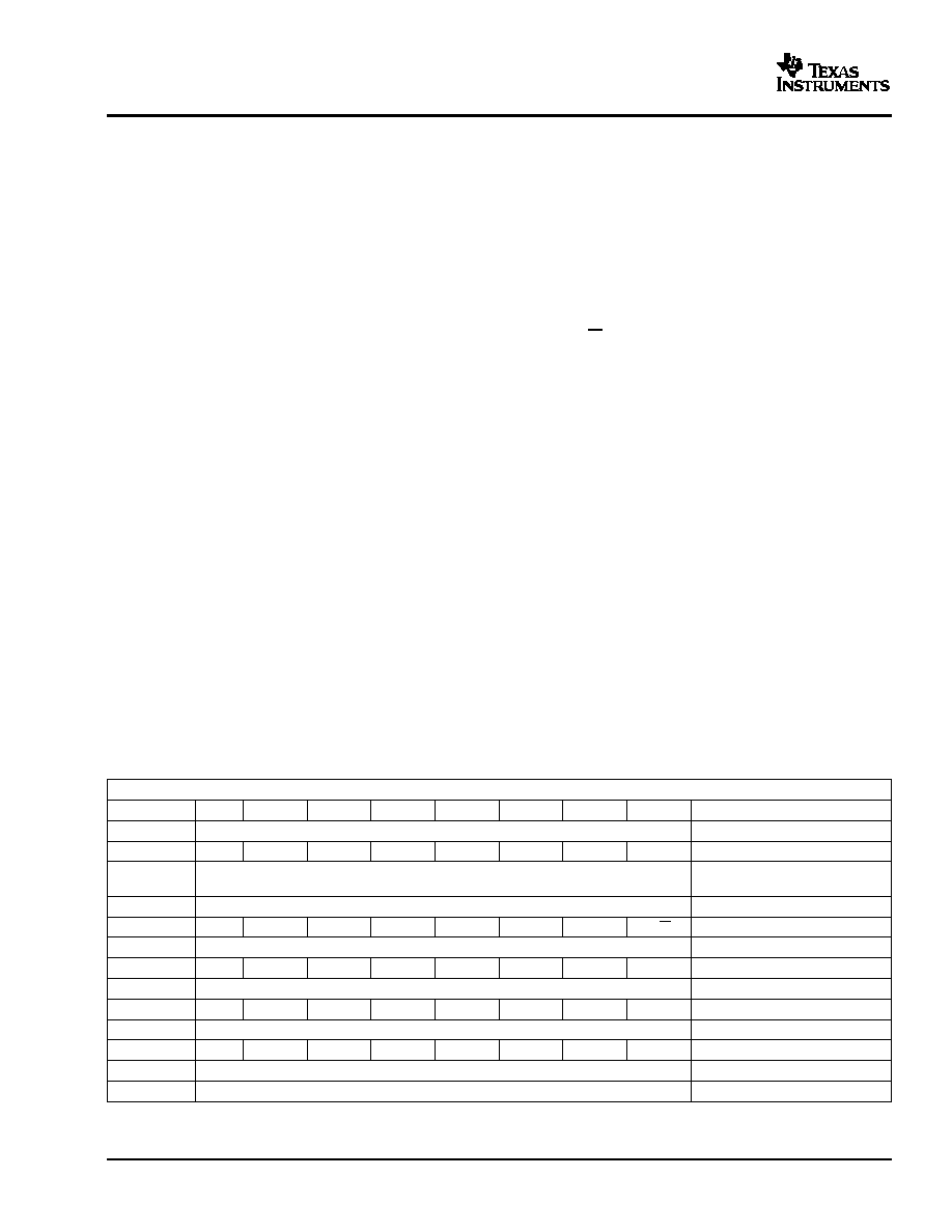
D/A SECTION
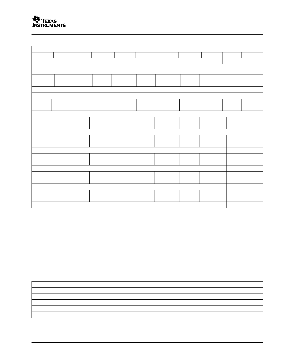
The architecture of the DAC8571 consists of a string DAC followed by an output buffer amplifier. Figure 27
shows a block diagram of the DAC architecture.
Figure 27. DAC8571 Architecture
The input coding to the DAC8571 is unsigned binary, which gives the ideal output voltage as:
where D = decimal equivalent of the binary code that is loaded to the DAC register; it can range from 0 to 65535.
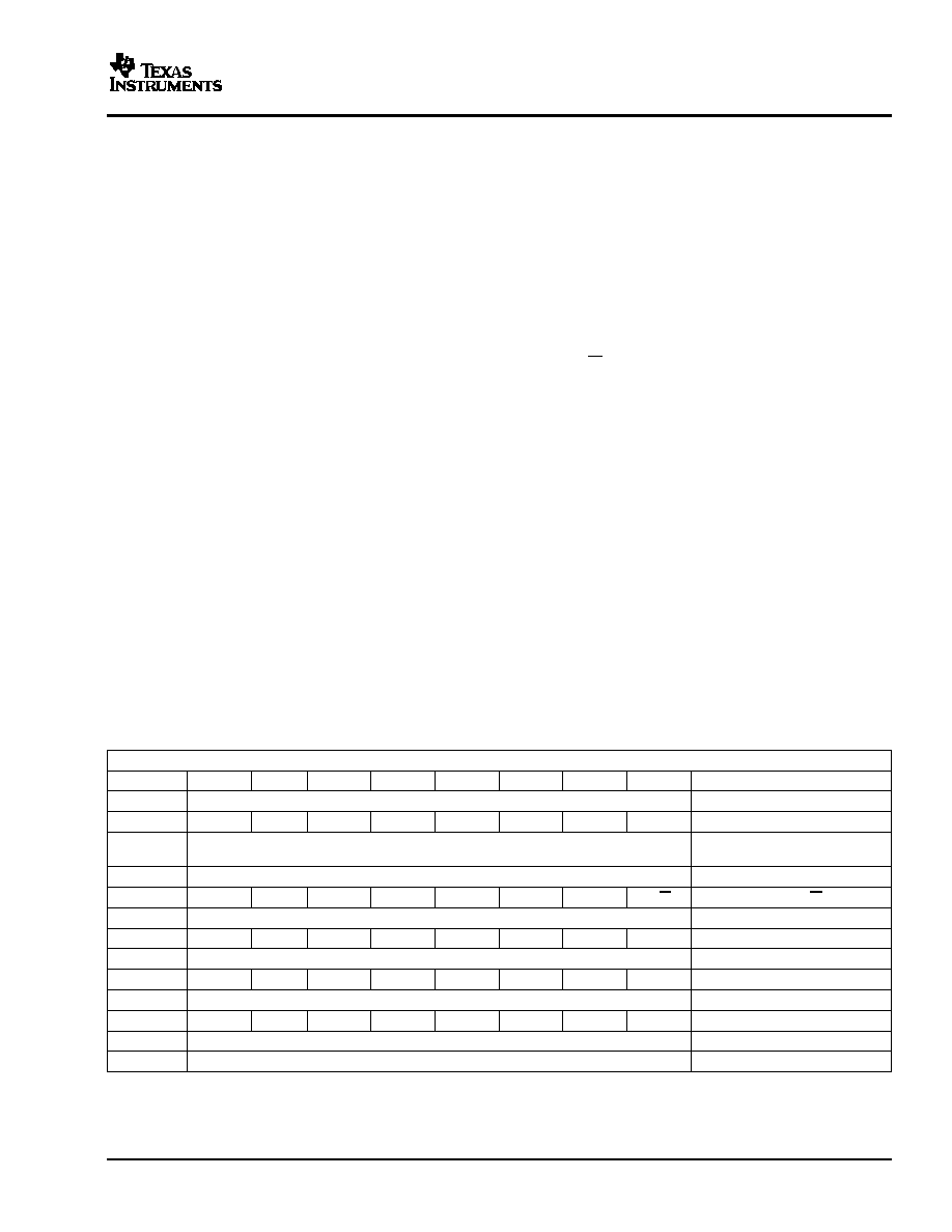
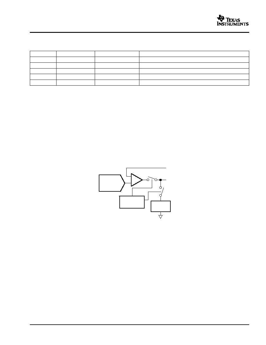
RESISTOR STRING
The resistor string section is shown in Figure 28. It is simply a divide-by-two resistor, followed by a string of
resistors, each of value R. The code loaded into the DAC register determines at which node on the string the
voltage is tapped off to be fed into the output amplifier by closing one of the switches connecting the string to the
amplifier. Because it is a string of resistors, it is assured monotonic.
Figure 28. Resistor String.
12
www.ti.com
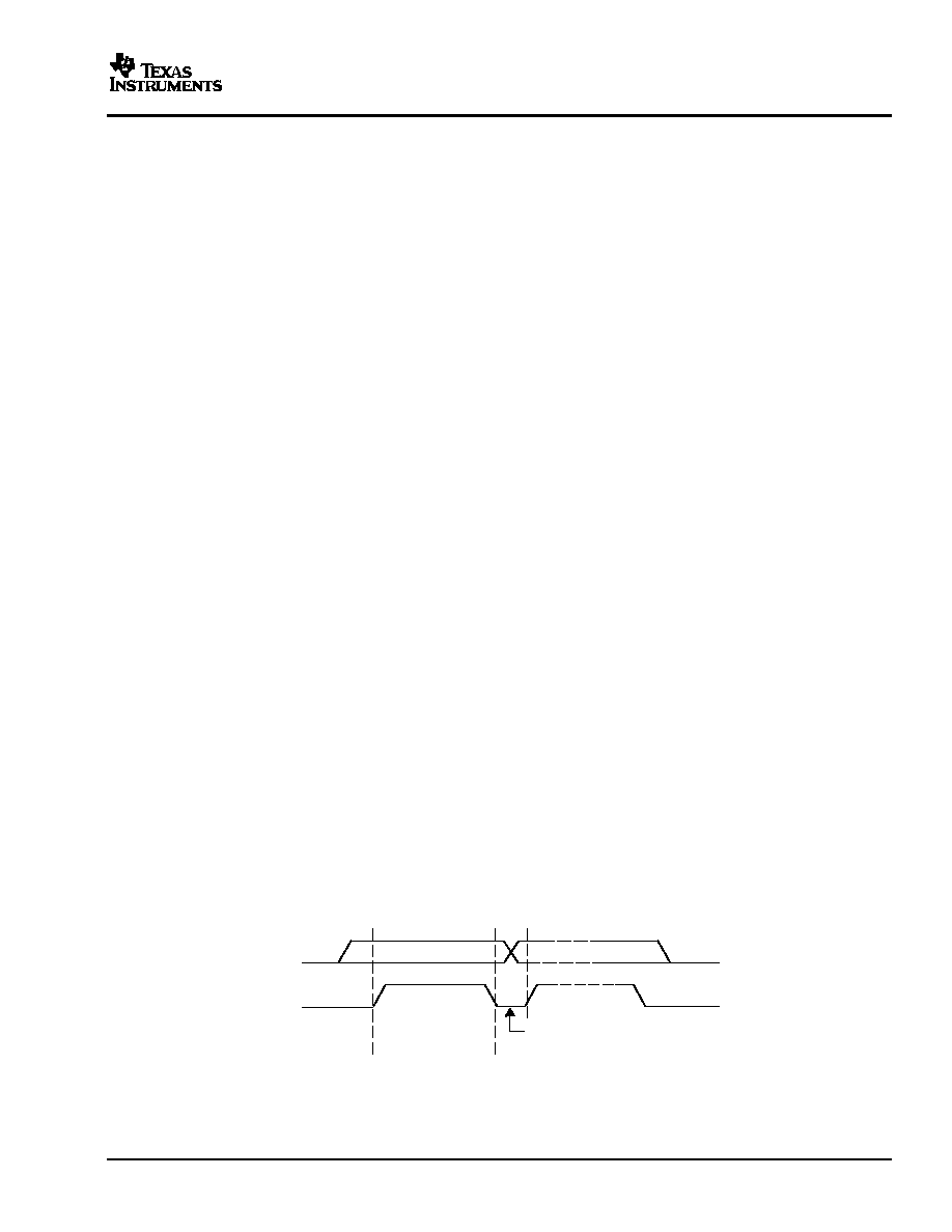
Change of Data Allowed
Data Line
Stable;
Data Valid
SDA
SCL
DAC8571
SLAS373A � DECEMBER 2002 � REVISED JULY 2003
THEORY OF OPERATION (continued)
Output Amplifier
The output buffer is a gain-of-2 noninverting amplifier capable of generating rail-to-rail voltages at its output,
which gives an output range of 0 V to V
DD
. It is capable of driving a load of 2 k
in parallel with 1000 pF to GND.
The source and sink capabilities (fast settling) of the output amplifier can be seen in the typical curves. The slew
rate is 1 V/�s with a full-scale settling time of 10 �s with the output loaded. The feedback and gain setting
resistors of the amplifier are in the order of 50 k
. Their absolute value can be off significantly, but they are
matched to within 0.1%.
The inverting input of the output amplifier is brought out to the VSENSE pin, through the feedback resistor. This
allows for better accuracy in critical applications by tying the VSENSE point and the amplifier output together
directly at the load. Other signal conditioning circuitry may also be connected between these points for specific
applications including current sourcing.
I
2
C Interface
The DAC8571 uses the I
2
C interface (see I
2
C-Bus Specification Version 2.1, January 2000, Philips
Semiconductor) to receive and transmit digital data. I
2
C is a 2-wire serial interface that allows multiple devices on
the same bus to communicate with each other. The serial bus consists of the serial data (SDA) and serial clock
(SCL) lines. Connections to the SDA and SCL lines of the bus are made through open drain IO pins of each
device on the bus. Since the devices that connect to the bus have open drain outputs, the bus should include
pullup structures. When the bus is not active, both SCL and SDA lines are pulled high by these pullup devices.
The DAC8571 supports the I
2
C serial bus and data transmission protocol, in all three defined modes: standard
(100 Kbps), fast (400 kBps), and high speed (3.4 Mbps).
I
2
C specification states that the device that controls the message is called a master, and the devices that are
controlled by the master are slaves. The master device generates the SCL signal. A master device also
generates special timing conditions (start condition, repeated start condition, and stop condition) on the bus to
indicate the start or stop of a data transfer. Device addressing is also done by the master. The master device on
an I
2
C bus is usually a microcontroller or a digital signal processor (DSP). The DAC8571 on the other hand,
operates as a slave device on the I
2
C bus. A slave device acknowledges master's commands and upon master's
control, either receives or transmits data.
I
2
C specification states that a device that sends data onto the bus is defined as a transmitter, and a device
receiving data from the bus is defined as a receiver. DAC8571 normally operates as a slave receiver. A master
device writes to DAC8571, a slave receiver. However, if a master device inquires DAC8571 internal register data,
DAC8571, operates as a slave transmitter. In this case, the master device reads from the DAC8571, a slave
transmitter. According to I
2
C terminology, read and write are with respect to the master device.
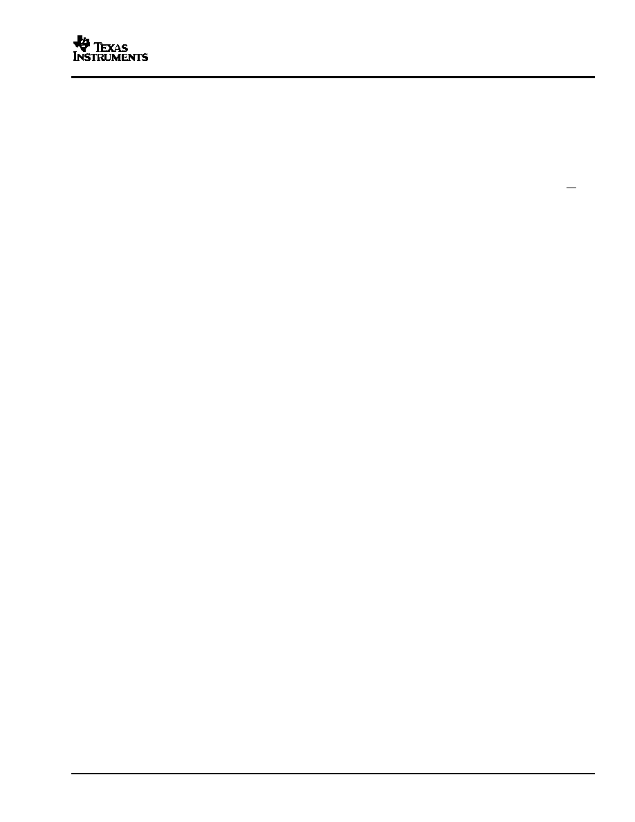
Other than specific timing signals, I
2
C interface works with serial bytes. At the end of each byte, a 9
th
clock cycle
is used to generate/detect an acknowledge signal. An acknowledge is when the SDA line is pulled low during the
high period of 9
th
clock cycle. A not-acknowledge is when SDA line is left high during the high period of the 9
th
clock cycle.
Figure 29. Valid Data
13
www.ti.com
Not Acknowledge
Acknowledge
1
2
8
9
Clock Pulse for
Acknowledgement
S
START
Condition
Data Output
by Transmitter
Data Output
by Receiver
SCL From
Master
Recognize START or
REPEATED START
Condition
Recognize STOP or
REPEATED START
Condition
Generate ACKNOWLEDGE
Signal
Acknowledgement
Signal From Slave
SDA
SCL
MSB
P
Sr
Sr
or
P
S
or
Sr
START or
Repeated START
Condition
STOP or
Repeated START
Condition
Clock Line Held Low While
Interrupts are Serviced
1
2
7
8
9
ACK
1
2
3 - 8
9
ACK
Address
R/W
DAC8571
SLAS373A � DECEMBER 2002 � REVISED JULY 2003
THEORY OF OPERATION (continued)
Figure 30. Acknowledge on the I
2
C Bus
Figure 31. Bus Protocol
14
www.ti.com
DAC8571
SLAS373A � DECEMBER 2002 � REVISED JULY 2003
THEORY OF OPERATION (continued)
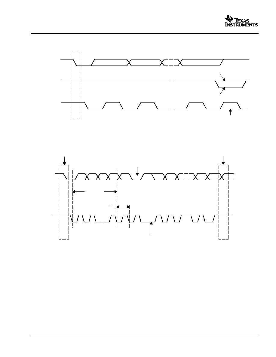
Master Writing to a Slave Receiver (Standard/Fast Modes)
I
2
C protocol starts when the bus is idle, that is, when SDA and SCL lines are stable high. The master then pulls
the SDA line low while SCL is still high indicating that serial data transfer has started. This is called a start
condition
, and can only be asserted by the master. After the start condition, the master generates the serial clock
pulses and puts out an address byte, ADDRESS<7:0>. While generating the bit stream, the master ensures the
timing for valid data. For each valid I
2
C bit, SDA line should remain stable during the entire high period of the
SCL line. The address byte consists of 7 address bits (1001100, assuming A0=0) and a direction bit (R/W=0).
After sending the address byte, the master generates a 9
th
SCL pulse and monitors the state of the SDA line
during the high period of this 9
th
clock cycle. The SDA line being pulled low by a receiver during the high period
of 9
th
clock cycle is called an acknowledge signal. If the master receives an acknowledge signal, it knows that a
DAC8571 successfully matched the address the master sent. Upon the receipt of this acknowledge, the master
knows that the communication link with a DAC8571 has been established and more data could be sent. The
master continues by sending a control byte C<7:0>, which sets DAC8571's operation mode. After sending the
control byte, the master expects an acknowledge signal. Upon receipt of the acknowledge, the master sends a
most significant byte
M<7:0> that represents the eight most significant bits of DAC8571's 16-bit digital-to-analog
conversion data. Upon receipt of the M<7:0>, DAC8571 sends an acknowledge. After receiving the acknowledge,
the master sends a least significant byte L<7:0> that represents the eight least significant bits of DAC8571's
16-bit conversion data. After receiving the L<7:0>, the DAC8571 sends an acknowledge. At the falling edge of
the acknowledge signal following the L<0>, DAC8571 performs a digital to analog conversion. For further DAC
updates, the master can keep repeating M<7:0> and L<7:0> sequences, expecting an acknowledge after each
byte. After the required number of digital-to-analog conversions is complete, the master can break the
communication link with DAC8571 by pulling the SDA line from low to high while SCL line is high. This is called a
stop condition
. A stop condition brings the bus back to idle (SDA and SCL both high). A stop condition indicates
that communication with DAC8571 has ended. All devices on the bus including DAC8571 then await a new start
condition followed by a matching address byte. DAC8571 stays at its current state upon receipt of a stop
condition. Table 1 demonstrates the sequence of events that should occur while a master transmitter is writing to
DAC8571.
15
www.ti.com
DAC8571
SLAS373A � DECEMBER 2002 � REVISED JULY 2003
THEORY OF OPERATION (continued)
Table 1. Master Transmitter Writing to Slave Receiver (DAC8571)
Standard/Fast Mode Write Sequence - Data Input
Transmitter
MSB
6
5
4
3
2
1
LSB
Comment
Master
Start
Begin sequence
Master
1
0
0
1
1
A0
0
R/W
Write addressing (LSB=0)
DAC8571
DAC8571 Acknowledges
Master
0
0
Load 1
Load 0
0
Brcsel
0
PD0
Control byte (PD0=0)
DAC8571
DAC8571 Acknowledges
Master
D15
D14
D13
D12
D11
D10
D9
D8
Writing dataword, high byte
DAC8571
DAC8571 Acknowledges
Master
D7
D6
D5
D4
D3
D2
D1
D0
Writing dataword, low byte
DAC8571
DAC8571 Acknowledges
Master
Stop or Repeated Start (1) (2)
Done
Standard/Fast Mode Write Sequence-Power Down Input
Transmitter
MSB
6
5
4
3
2
1
LSB
Comment
Master
Start
Begin sequence
Master
1
0
0
1
1
A0
0
R/W
Write addressing (LSB=0)
DAC8571
DAC8571 Acknowledges
Master
0
0
Load 1
Load 0
0
Brcsel
0
PD0
Control byte (PD0=1)
DAC8571
DAC8571 Acknowledges
Master
PD1
PD2
PD3
0
0
0
0
0
Writing dataword, high byte
DAC8571
DAC8571 Acknowledges
Master
0
0
0
0
0
0
0
0
Writing dataword, low byte
DAC8571
DAC8571 Acknowledges
Master
Stop or Repeated Start (3) (4)
Done
(1)
High byte, low byte sequence can repeat.
(2)
Use repeated start to secure bus operation and loop back to the stage of write addressing for next Write.
(3)
High byte, low byte sequence can repeat.
(4)
Use repeated start to secure bus operation and loop back to the stage of write addressing for next Write.
16
www.ti.com
DAC8571
SLAS373A � DECEMBER 2002 � REVISED JULY 2003
THEORY OF OPERATION (continued)
Master Reading From a Slave Transmitter (Standard/Fast Modes)
I
2
C protocol starts when the bus is idle, that is, when SDA and SCL lines are stable high. The master then pulls
the SDA line low while SCL is still high indicating that serial data transfer has started. This is called a start
condition
, and can only be asserted by the master. After the start condition, the master generates the serial clock
pulses and puts out an address byte, ADDRESS<7:0>. While generating the bit stream, the master ensures the
timing for valid data. For each valid I
2
C bit, SDA line should remain stable during the entire high period of the
SCL line. The address byte consists of seven address bits (1001100, assuming A0=0) and a direction bit
(R/W=1). After sending the address byte, the master generates a 9
th
SCL pulse and monitors the state of the
SDA line during the high period of this 9
th
clock cycle (master leaves the SDA line high). The SDA line being
pulled low by a receiver during the high period of 9
th
clock cycle is called an acknowledge signal. If the master
receives an acknowledge signal, it knows that a DAC8571 successfully matched the address the master sent.
Since the R/W bit in the address byte was set, master also knows that DAC8571 is ready to transmit data. Upon
the receipt of this acknowledge, the master knows that the communication link with a DAC8571 has been
established and more data could be received. The master continues by sending eight clock cycles during which
DAC8571 transmits a most significant byte, M<7:0>. If the master detects all bits of the M<7:0> as valid data, it
sends an acknowledge signal in the 9
th
cycle. DAC8571 detects this acknowledge signal and prepares to send
more data. Upon the receipt of eight clock cycles from the master, DAC8571 transmits the least significant byte
L<7:0>. If the master detects all bits of the L<7:0> as valid data, it sends an acknowledge signal to DAC8571
during the 9
th
clock cycle. DAC8571 detects this acknowledge signal and prepares to send more data. Upon the
receipt of 8 more clock cycles from the master, DAC8571 transmits the control byte C<7:0>. During the 9
th
clock
cycle, the master transmits a not-acknowledge signal to DAC8571 and terminates the sequence with a stop
condition, by pulling the SDA line from low to high while clock is high. M<7:0> and L<7:0> data could be either
DAC data or could be the data stored in the temporary register. Bits in the C<7:0> reveal this information.
Table 2 demonstrates the sequence of events that should occur while a master receiver is reading from
DAC8571.
Table 2. Master Receiver Reads From Slave Transmitter (DAC8571)
Standard/Fast Mode Read Sequence-Data Transmit
Transmitter
MSB
6
5
4
3
2
1
LSB
Comment
Master
Start
Begin sequence
Master
1
0
0
1
1
A0
0
R/W
Read addressing (R/W = 1)
DAC8571
DAC8571 Acknowledges
DAC8571
D15
D14
D13
D12
D11
D10
D9
D8
High byte
Master
Master Acknowledges
DAC8571
D7
D6
D5
D4
D3
D2
D1
D0
Low byte
Master
Master Acknowledges
DAC8571
C7
C6
C5
C4
C3
C2
C1
C0
Control byte
Master
Master Not Acknowledges
Master signal end of read
Master
Stop or Repeated Start
Done
Master Writing to a Slave Receiver (High-Speed Mode)
All devices must start operation in standard/fast mode and switch to high-speed mode using a well defined
protocol. This is required because high-speed mode requires the on chip filter settings of each I
2
C device (for
SDA and SCL lines) to be switched to support 3.4 Mbps operation. A stop condition always ends the high speed
mode and puts all devices back to standard/fast mode.
17
www.ti.com
DAC8571
SLAS373A � DECEMBER 2002 � REVISED JULY 2003
THEORY OF OPERATION (continued)
I
2
C protocol starts when the bus is idle, that is, when SDA and SCL lines are stable high. The master then pulls
the SDA line low while SCL is still high indicating that serial data transfer has started. This is called a start
condition
, and can only be asserted by the master. After the start condition, the master device puts out the
high-speed master code 0000 1xxx. No device is allowed to acknowledge the master code, but the devices are
required to switch their internal settings to support 3.4 Mbps operation upon the receipt of this code. After the
not-acknowledge signal, the master is allowed to operate at high speed. Now at much higher speed, the master
generates a repeated start condition. After the start condition, master generates the serial clock pulses and puts
out an address byte, ADDRESS<7:0>. While generating the bit stream, the master ensures the timing for valid
data. For each valid I
2
C bit, SDA line should remain stable during the entire high period of the SCL line. The
address byte consists of seven address bits and a direction bit (R/W=0). After sending the address byte, the
master generates a 9
th
SCL pulse and monitors the state of the SDA line during the high period of this 9th clock
cycle (master leaves the SDA line high). The SDA line being pulled low by the receiver during the high period of
9
th
clock cycle is called an acknowledge signal. If the master receives an acknowledge signal, it knows that a
DAC8571 successfully matched the address the master sent. Upon the receipt of this acknowledge, the master
knows that the high-speed communication link with a DAC8571 has been established and more data could be
sent. The master continues by sending a control byte, C<7:0>, which sets DAC8571 operation mode. After
sending the control byte, master expects an acknowledge. Upon the receipt of an acknowledge, the master
sends a most significant byte, M<7:0> that represents the eight most significant bits of DAC8571's 16-bit
digital-to-analog conversion data. Upon the receipt of the M<7:0>, DAC8571 sends an acknowledge. After
receiving the acknowledge, the master sends a least significant byte, L<7:0>, that represents the eight least
significant bits of DAC8571's 16-bit conversion data. After receiving the L<7:0>, the DAC8571 sends an
acknowledge. At the falling edge of the acknowledge signal following the L<0>, DAC8571 performs a digital to
analog conversion, depending on the operational mode. For further DAC updates, the master can keep repeating
M<7:0> and L<7:0> sequences, expecting an acknowledge after each byte. After the required number of digital
to analog conversions is complete, the master can break the communication link with DAC8571 by pulling the
SDA line from low to high while SCL line is high. This is called a stop condition. A stop condition brings the bus
back to idle (SDA and SCL both high). A stop condition indicates that communication with a device (DAC8571)
has ended. All devices on the bus including DAC8571 then await a new start condition followed by a matching
address byte. DAC8571 stays at its current state upon the receipt of a stop condition. A stop condition during the
high-speed mode also indicates the end of the high-speed mode. Table 3 demonstrates the sequence of events
that should occur while a master transmitter is writing to DAC8571 in I
2
C high-speed mode.
Table 3. Master Transmitter Writes to Slave Receiver in High-Speed Mode
HS Mode Write Sequence-Data Input
Transmitter
MSB
6
5
4
3
2
1
LSB
Comment
Master
Start
Begin sequence (1)
Master
0
0
0
0
1
X
X
X
HS mode master code
No device may acknowledge HS
NONE
Not Acknowledge
master code
Master
Repeated Start
Master
1
0
0
1
1
A0
0
R/W
Write addressing (LSB = 0)
DAC8571
DAC8571 Acknowledges
Master
0
0
Load 1
Load 0
0
Brcsel
0
PD0
Control byte (PD0=0)
DAC8571
DAC8571 Acknowledges
Master
D15
D14
D13
D12
D11
D10
D9
D8
Writing dataword, high byte
DAC8571
DAC8571 Acknowledges
Master
D7
D6
D5
D4
D3
D2
D1
D0
Writing dataword, low byte
DAC8571
DAC8571 Acknowledges
Master
Stop or Repeated Start (2)
Done
(1)
High-byte, low-byte sequences can repeat
(2)
Use repeated start to secure bus operation and loop back to the stage of write addressing for next Write.
18
www.ti.com
DAC8571
SLAS373A � DECEMBER 2002 � REVISED JULY 2003
THEORY OF OPERATION (continued)
Master Receiver Reading From a Slave Transmitter (High-Speed Mode)
I
2
C protocol starts when the bus is idle, that is, when SDA and SCL lines are stable high. The master then pulls
the SDA line low while SCL is still high indicating that serial data transfer has started. This is called a start
condition
, and can only be asserted by the master. After the start condition, the master device puts out the
high-speed master code 0000 1xxx. No device is allowed to acknowledge the master code, but the devices are
required to switch their internal settings to support 3.4 Mbps operation upon the receipt of this code. After the
not-acknowledge signal, the master is allowed to operate at high speed. Now at much higher speed, the master
generates a repeated start condition. After the start condition, the master generates the serial clock pulses and
puts out an address byte, ADDRESS<7:0>. While generating the bit stream, the master ensures the timing for
valid data. For each valid I
2
C bit, SDA line should remain stable during the entire high period of the SCL line. The
address byte consists of seven address bits and a direction bit (R/W=1). After sending the address byte, the
master generates a 9
th
SCL pulse and monitors the state of the SDA line during the high period of this 9
th
clock
cycle (master leaves the SDA line high). The SDA line being pulled low by the receiver during the high period of
9
th
clock cycle is called an acknowledge signal. If the master receives an acknowledge signal, it knows that a
DAC8571 successfully matched the address the master sent. Since the R/W bit in the address byte was set,
master also knows that DAC8571 is ready to transmit data. Upon the receipt of this acknowledge, the master
knows that the communication link with a DAC8571 has been established and more data could be received. The
master continues by sending eight clock cycles during which DAC8571 transmits an M<7:0>. If the master
detects all bits of the M<7:0> as valid data, it sends an acknowledge signal in the 9
th
cycle. DAC8571 detects
this acknowledge signal and prepares to send more data. Upon the receipt of eight more clock cycles from the
master, DAC8571 transmits L<7:0>. If the master detects all bits of the L<7:0> as valid data, it sends an
acknowledge signal to DAC8571 during the 9th clock cycle. DAC8571 detects this acknowledge signal and
prepares to send more data. Upon the receipt of eight more clock cycles from the master, DAC8571 transmits
the control byte, C<7:0>. In the 9th clock cycle the master transmits a not-acknowledge signal to DAC8571 and
terminates the sequence with a stop condition, by pulling the SDA line from low to high while clock is high.
M<7:0> and L<7:0> data could be either DAC data or could be the data stored in the temporary register. Bits in
the C<7:0> reveal this information. A stop condition during the high-speed mode also indicates the end of the
high-speed mode. Table 4 demonstrates the sequence of events that should occur while a master receiver is
reading from DAC8571 in I
2
C high-speed mode.
Table 4. Master Receiver Reads Data From Slave Transmitter in High-Speed Mode
HS Mode Read Sequence-Data Transmit
Transmitter
MSB
6
5
4
3
2
1
LSB
Comment
Master
Start
Begin sequence
Master
0
0
0
0
1
X
X
X
HS Mode master code
No device may acknowledge HS
NONE
Not Acknowledge
master code
Master
Repeated Start
Master
1
0
0
1
1
A0
0
R/W
Read addressing (R/W=1)
DAC8571
DAC8571 Acknowledges
DAC8571
D15
D14
D13
D12
D11
D10
D9
D8
High byte
Master
Master Acknowledges
DAC8571
D7
D6
D5
D4
D3
D2
D1
D0
Low byte
Master
Master Acknowledges
DAC8571
C7
C6
C5
C4
C3
C2
C1
C0
Control byte
Master
Master Not Acknowledges
Master signal end of read
Master
Stop or Repeated Start (1)
Done
(1)
Use repeated start to secure bus operation and loop back to the stage of write addressing for next Write.
19
www.ti.com
DAC8571
SLAS373A � DECEMBER 2002 � REVISED JULY 2003
THEORY OF OPERATION (continued)
DAC8571 Update Sequence
DAC8571 requires a start condition, a valid I
2
C address, a control byte, an MS byte and an LS byte for an
update. The control byte sets the operational mode of the DAC8571. After the receipt of the control byte,
DAC8571 expects an MS byte and an LS byte. After the receipt of each byte, DAC8571 acknowledges by pulling
the SDA line low. At the falling edge of the acknowledge signal that follows the LS byte, DAC8571 performs an
update.
After the first update, further data can be sent as MS byte and LS byte sequences and DAC8571 keeps updating
at the falling edge of the acknowledge signal that follows each LS byte. The bits of the last control byte
determine the type of update being performed. Thus, for the first update, DAC8571 requires a start condition, a
valid I
2
C address, a control byte, an MS byte and an LS byte. For all consecutive updates, DAC8571 needs an
MS byte and an LS byte.
Using the I
2
C high-speed mode, the clock running a 3.4 MHz, each 16-bit DAC update can be done within
18-clock cycles (MS byte, acknowledge bit, LS byte, acknowledge bit), at 188.88 KSPS. Using the fast mode,
clock running at 400 kHz, maximum DAC update rate is limited to 22.22 KSPS.
DAC8571 Address Byte
MSB
LSB
1
0
0
1
1
A0
0
R/W
The address byte is the first byte received following a START condition from the master device. The first five bits
(MSBs) of the slave address are factory preset to 10011. The next bit of the address byte is the device select bit
A0, followed by a fixed 0 and the read/write direction bit R/W. In order for DAC8571 to respond, the 7-bit address
should be 10011A00, where the state of the A0 bit matches the state of the A0 pin. A maximum of two DAC8571
devices with the same preset code can therefore be connected on the same bus at one time. The A0 Address
inputs can be permanently connected to VDD or digital ground, or can be actively driven by TTL or CMOS logic
levels. The device address is set by the state of these pins upon power up of the DAC8571. The last bit of the
address byte (R/W) defines the direction of the data flow. When set to a 1, a read operation is selected (master
device reads from DAC8571); when set to a 0, a write operation is selected (master device writes to DAC8571).
Following the START condition, the DAC8571 monitors the SDA bus, checking the device address being
transmitted. Upon receiving the 10011A00 code, and the R/W bit, the DAC8571 outputs an acknowledge signal
on the SDA line.
Broadcast addressing is also supported by DAC8571. Broadcast addressing can be used for synchronously
updating or powering down multiple DAC8571 devices on the same bus. DAC8571 is designed to work with other
members of DAC857x, DAC757x families to support multichannel synchronous update. When broadcast
addressing is used, DAC8571 responds regardless of the state of the A0 pin. Broadcast address is only valid for
write operation and cannot be used for read operation. Broadcast address is as follows.
MSB
LSB
1
0
0
1
0
0
0
0
Control Byte
After transmitting an acknowledge pulse following a valid address, DAC8571 expects a control byte C<7:0>.
Control byte functionality is shown in Table 5.
The first two MSBs C<7> and C<6> of the control byte must be zeroes for DAC8571 to update. If these two bits
are not assigned to zero, DAC8571 ignores all update commands, but still generates an acknowledge signal.
C<5> and C<4> are used for setting the update mode. Some of these modes are designed to support
multichannel synchronous operation between multiple devices.
20
www.ti.com
DAC8571
SLAS373A � DECEMBER 2002 � REVISED JULY 2003
THEORY OF OPERATION (continued)
�
C<5>=0, C<4>=0: Store I
2
C data. The contents of MS byte and LS byte data (or power-down information)
are stored into the temporary register. This mode does not change the DAC output.
�
C<5>=0, C<4>=1: Update DAC with I
2
C data. Most common mode. The contents of MS byte and LS byte
data (or power-down information) are stored into the temporary data register and into the DAC register. This
mode changes the DAC output with the contents of I
2
C MS byte and LS byte data.
�
C<5>=1, C<4>=0: Update with previously stored data. The contents of MS byte and LS byte data (or
power-down information) are ignored. The DAC is updated with the contents of the data previously stored in
the temporary register. This mode changes the DAC output.
�
C<5>=1, C<4>=1: Broadcast update, If C<2>=0, DAC is updated with the contents of its temporary register.
If C<2>=1, DAC is updated with I
2
C MS byte and LS byte data. C<7> and C<6> do not have to be zeroes in
order for DAC8571 to update. This mode is intended to help DAC8571 work with other DAC857x and
DAC757x devices for multichannel synchronous update applications.
C<3> should always be zero.
C<2> is utilized only when C<5>=C<4>=1. Otherwise, C<2> must be assigned to zero.
C<1> should always be zero.
C<0> should be zero during normal DAC operation. C<0>=1 is a power-down flag. If C<0>=1, M<7>, M<6>, and
M<5> indicate a powerdown operation as shown in Table 6.
Table 5. Control Byte Functionality
C<7>
C<6>
C<5>
C<4>
C<3>
C<2>
C<1>
C<0>
M<7>
M<6>
M<5>
Load1 Load0
Brcsel
PD0
MSB
MSB-1
MSB-2...LSB
DAC8571 FUNCTION
0
0
0
0
0
0
0
0
Data
Write temporary register with data
Write temporary register with power
0
0
0
0
0
0
0
1
See Table 6
down command
Write temporary register and load
0
0
0
1
0
0
0
0
Data
DAC with data
0
0
0
1
0
0
0
1
See Table 6
Power down DAC
Update DAC with temporary register
0
0
1
0
0
0
0
0
x
data or power down
Broadcast Commands
Load all DACs, all devices with tem-
x
x
1
1
x
0
x
x
x
porary register data
x
x
1
1
x
1
x
0
Data
Load all DACs, all devices with data
x
x
1
1
x
1
x
1
See Table 6
Power down all DACs, all devices
Most Significant Byte
Most Significant Byte M<7:0> consists of 8 most significant bits of D/A conversion data. When C<0>=1. M<7>,
M<6>, M<5> indicate a powerdown operation as shown in Table 6.
Least Significant Byte
Least Significant Byte L<7:0> consists of the 8 least significant bits of D/A conversion data. DAC8571 updates at
the falling edge of the acknowledge signal that follows the L<0> bit.
Data Transmit and Read-Back
I
2
C bus can be noisy and data integrity and can be a problem in a system of many I
2
C devices. To enable I
2
C
system verification, DAC8571 provides read back capability for the user. During read back operation, the
contents of the control byte, MS byte and the LS byte can be sent back to the master device using the I
2
C bus.
This read-back function is also useful if a device on the I
2
C bus inquires DAC8571 data.
21

www.ti.com
DAC8571
SLAS373A � DECEMBER 2002 � REVISED JULY 2003
THEORY OF OPERATION (continued)
For read-back operation, the master device sends the I
2
C address and sets the R/W bit. DAC8571
acknowledges. Then, upon the receipt of clock pulses from the master, DAC8571 sends the MS byte. If the
master acknowledges, DAC8571 sends the LS byte. If the master acknowledges, DAC8571 sends the control
byte. This sequence is interrupted by the master sending a not acknowledge signal.
Depending on the contents of the control byte transmitted by the DAC8571, the MS byte and LS byte information
(transmitted by the DAC8571) is interpreted as follows:
C<5>
C<4>
C<2>
0
0
0
MS and LS bytes represent temporary register data
0
1
0
MS and LS bytes represent temporary and DAC register data
1
0
0
MS and LS bytes represent I
2
C data that is discarded
1
1
0
MS and LS bytes represent I
2
C data that is discarded
1
1
1
MS and LS bytes represent temporary and DAC register data
EXAMPLES (A0 TIED TO GND, VDD = 5 V)
EXAMPLE 1: Write 1/4 scale to DAC8571
ADDRESS <7...0>
C<7...0>
M<7...0>
L<7...0>
START
1001 1000
ACK
0001 0000
ACK
0100 0000
ACK
0000 0000
ACK
STOP
Previous output voltage is valid
Vout = 1.25 V
EXAMPLE 2: Switch DAC8571 to fast settling mode
ADDRESS <7...0>
C<7...0>
M<7...0>
L<7...0>
START
1001 1000
ACK
0001 0001
ACK
0010 0000
ACK
0000 0000
ACK
STOP
Previous output voltage is valid
Vout = 0 V
EXAMPLE 3: Switch DAC8571 back to low power mode
ADDRESS <7...0>
C<7...0>
M<7...0>
L<7...0>
START
1001 1000
ACK
0001 0001
ACK
0000 0000
ACK
0000 0000
ACK
STOP
Previous output voltage is valid
Vout = 0 V
EXAMPLE 4: Power-down DAC8571 with Hi-Z output
ADDRESS <7...0>
C<7...0>
M<7...0>
L<7...0>
START
1001 1000
ACK
0001 0001
ACK
1100 0000
ACK
0000 0000
ACK
STOP
Previous output voltage is valid
Vout = Hi-Z
EXAMPLE 5: Power-down DAC8571 with 1K output impedance to ground
ADDRESS <7...0>
C<7...0>
M<7...0>
L<7...0>
START
1001 1000
ACK
0001 0001
ACK
0100 0000
ACK
0000 0000
ACK
STOP
Previous output voltage is valid
Vout = 0 V
EXAMPLE 6: Power-down DAC8571 with 100K output impedance to ground
ADDRESS <7...0>
C<7...0>
M<7...0>
L<7...0>
START
1001 1000
ACK
0001 0001
ACK
1000 0000
ACK
0000 0000
ACK
STOP
Previous output voltage is valid
Vout = 0 V
EXAMPLE 7: Store full scale data in temporary register
ADDRESS <7...0>
C<7...0>
M<7...0>
L<7...0>
START
1001 1000
ACK
0000 0000
ACK
1111 1111
ACK
1111 1111
ACK
STOP
Previous output voltage is valid
EXAMPLE 8: Update DAC8571 with the data previously stored in the temporary register
ADDRESS <7...0>
C<7...0>
M<7...0>
L<7...0>
START
1001 1000
ACK
0010 0000
ACK
XXXX XXXX
ACK
XXXX XXXX
ACK
STOP
Previous output voltage is valid
New Vout valid
EXAMPLE 9: Broadcast a powerdown command to all DAC8571s on the I
2
C bus
ADDRESS <7...0>
C<7...0>
M<7...0>
L<7...0>
22
www.ti.com
DAC8571
SLAS373A � DECEMBER 2002 � REVISED JULY 2003
THEORY OF OPERATION (continued)
EXAMPLE 9: Broadcast a powerdown command to all DAC8571s on the I
2
C bus
START
1001 0000
ACK
0011 0101
ACK
1100 0000
ACK
0000 0000
ACK
STOP
Previous output voltage is valid
Vout = Hi-Z
EXAMPLE 10: Broadcast update. All DAC8571s on the I
2
C bus update synchronously with the contents of their temporary
registers
ADDRESS <7...0>
C<7...0>
M<7...0>
L<7...0>
START
1001 0000
ACK
0011 0000
ACK
XXXX XXXX
ACK
XXXX XXXX
ACK
STOP
Previous output voltage is valid
New Vout valid
EXAMPLE 11: Read back DAC8571 internal data. V denotes valid logic.
ADDRESS<7...0>
M<7...0>
MASTER
L<7...0>
MASTER
C<7...0>
MASTER
START
1001 1001
ACK
VVVV VVVV
ACK
VVVV VVVV
ACK
VVVV VVVV NOT ACK STOP
EXAMPLE 12: Ramp generation in high speed mode (up to code 7 is shown)
HS Master Code
ADDRESS
C<7...0>
START
0000 1000
NOT ACK
REPEATED START
1001 1000
ACK
0001 0000
ACK
Previous Vout voltage valid
MSB<7...0>
LSB<7...0>
MSB<7...0>
LSB<7...0>
0000 0000
ACK
0000 0000
ACK
0000 0000
ACK
0000 0001
ACK
Previous Vout voltage valid
Vout = 0 V
Vout = 76 �V
MSB<7...0>
LSB<7...0>
MSB<7...0>
LSB<7...0>
0000 0000
ACK
0000 0010
ACK
0000 0000
ACK
0000 0011
ACK
Vout = 76 �V
Vout = 2
�76 �V
Vout = 3
�76 �V
MSB<7...0>
LSB<7...0>
MSB<7...0>
LSB<7...0>
0000 0000
ACK
0000 0100
ACK
0000 0000
ACK
0000 0101
ACK
Vout = 3
�76 �V
Vout = 4
�76 �V
Vout = 5
�76 �V
MSB<7...0>
LSB<7...0>
MSB<7...0>
LSB<7...0>
0000 0000
ACK
0000 0110
ACK
0000 0000
ACK
0000 0111
ACK
Vout = 5
�76 �V
Vout = 6
�76 �V
Vout = 7
�76 �V
Power-On Reset
The DAC8571 contains a power-on-reset circuit that controls the output voltage during power-up. On power-up,
the DAC register is filled with zeros and the output voltage is 0V; it remains there until a valid write sequence is
made to the DAC. This is useful in applications where it is important to know the state of the output of the DAC
while it is in the process of powering up. No input is brought high before the power is applied.
Power-Down Modes
The DAC8571 contains five separate power settings. These modes are programmable when C<0>=1. When
C<0>=1, M<7>, M<6>, and M<5> bits represent power setting control bits, and M<4...0> and L<7...0> are
assigned to zeroes. Power setting of DAC8571 is updated at the falling edge of the acknowledge signal that
follows the least significant byte. To set the power consumption of the device, following I
2
C sequence is used.
Start_condition ->
Valid_address
(1001 1000) -> ack
C<7:0>
(0001 0001) -> ack
M<7:0>
( vvv0 0000) -> ack
L<7:0>
(0000 0000) -> ack
Stop_condition
23
www.ti.com
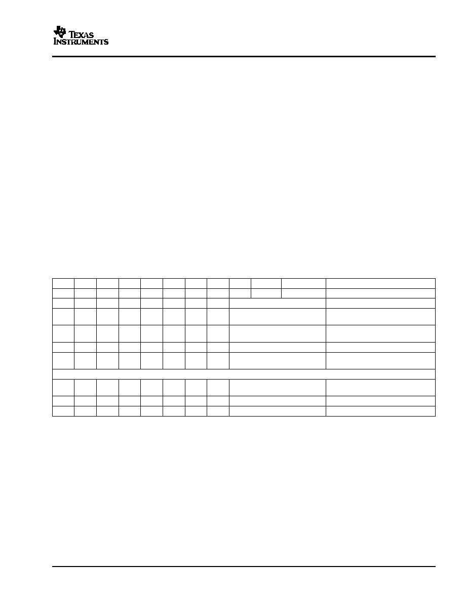
_
+
Resistor
String DAC
Powerdown
Circuitry
V
Sense
V
OUT
Amplifier
Resistor
Network
DAC8571
SLAS373A � DECEMBER 2002 � REVISED JULY 2003
THEORY OF OPERATION (continued)
Table 6. Power Settings for the DAC8571 (C<0>=1)
M<7>
M<6>
M<5>
Operating Mode
0
0
0
Low power mode, default
0
0
1
Fast settling mode
0
1
X
PWD. 1k
to GND
1
0
X
PWD. 100 k
to GND
1
1
X
PWD. Output Hi-Z
After power-up, the device works in low power mode with its normal power consumption of 170 �A at 5 V. At fast
settling mode, device consumes 250 �A nominally, but settles in 10 �s. For the three power-down modes, the
supply current falls to 200 nA at 5 V (50 nA at 3 V). Not only does the supply current fall but the output stage is
also internally switched from the output of the amplifier to a resistor network of known values. This has the
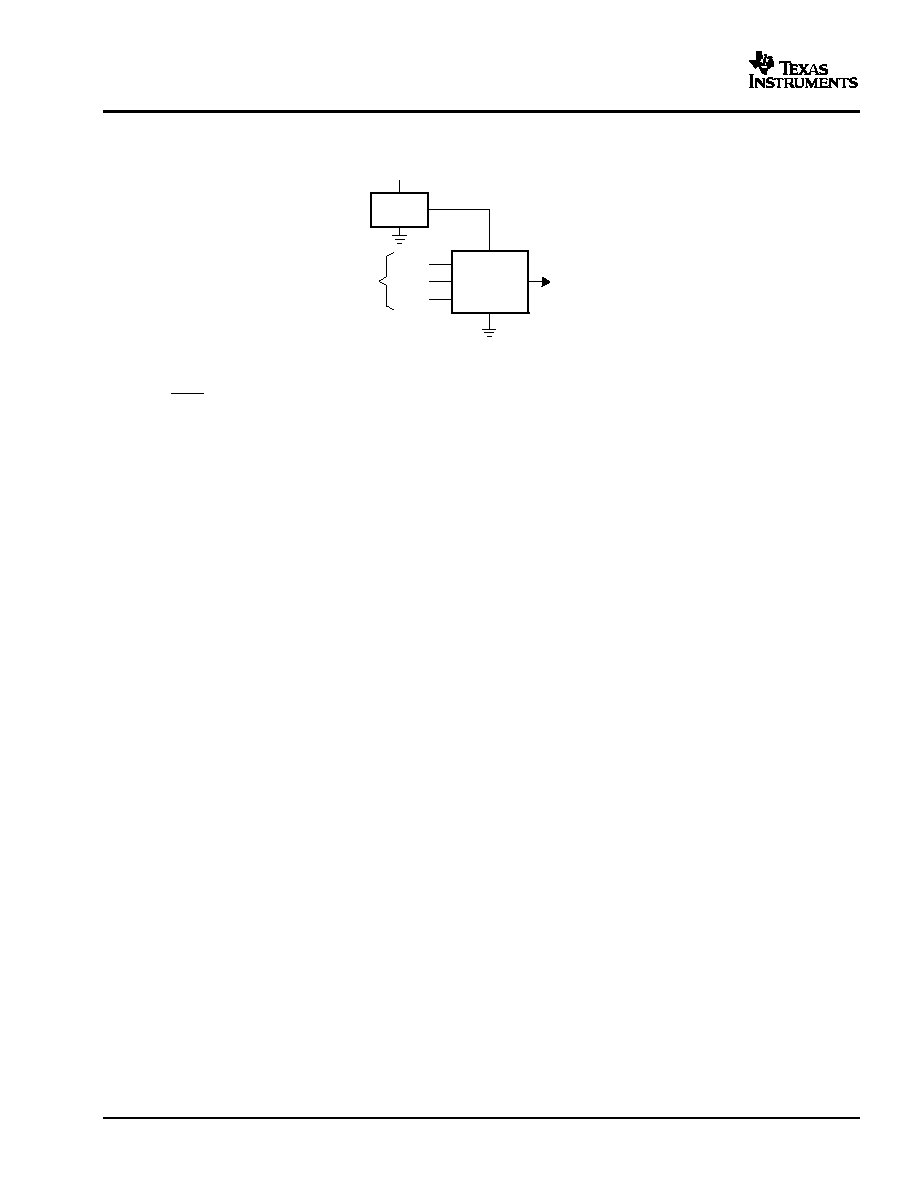
advantage that the output impedance of the device is known while in power-down mode. There are three
different options: The output is connected internally to GND through a 1-k
resistor, a 100-k resistor or it is left
open-circuit (high impedance). The output stage is illustrated in Figure 32.
A power on reset starts the DAC8571 in the low power mode. Low power mode and fast-settling mode settings
stay unchanged during DAC8571 data updates, unless they are specifically overwritten as explained in Table 6.
On the other hand, each new data sequence requiring a DAC update brings the DAC8571 out of the three
power-down conditions.
DAC8571 power settings can be stored in the temporary register, just like data (use C<7:0> = 0000 0001). This
allows simultaneous powerdown capability for multichannel applications.
Figure 32. Output Stage During Power-Down
All linear circuitry is shut down when the power-down mode is activated. However, the contents of the DAC
register are unaffected when in power-down. The time to exit power-down is typically 2.5 �s for V
DD
= 5 V and
5 �s for V
DD
= 3 V. (See the Typical Characteristics section for additional information.)
CURRENT CONSUMPTION
In the low power mode, the DAC8571 typically consumes 170 �A at V
DD
= 5 V and 150 �A at V
DD
= 3 V including
reference current consumption. Fast settling mode adds 80 �A of current consumption, but ensures 10-�s
settling. Additional current consumption can occur at the digital inputs if VIH<<VDD. For most efficient power
operation, CMOS logic levels are recommended at the digital inputs to the DAC. In power-down mode, typical
current consumption is 200 nA.
24

www.ti.com
DAC8571
SLAS373A � DECEMBER 2002 � REVISED JULY 2003
THEORY OF OPERATION (continued)
DRIVING RESISTIVE AND CAPACITIVE LOADS
The DAC8571 output stage is capable of driving loads of up to 1000 pF while remaining stable. Within the offset
and gain error margins, the DAC8571 can operate rail-to-rail when driving a capacitive load. Resistive loads of 2
k
can be driven by the DAC8571 while achieving a very good load regulation. Load regulation error increases
when the DAC output voltage is close to supply rails. When the outputs of the DAC are driven to the positive rail
under resistive loading, the PMOS transistor of each Class-AB output stage can enter into the linear region.
When this occurs, the added IR voltage drop deteriorates the linearity performance of the DAC. This only occurs
within approximately the top 20 mV of the DAC's digital input-to-voltage output transfer characteristic. The
reference voltage applied to the DAC8571 may be reduced below the supply voltage applied to VDD in order to
eliminate this condition if good linearity is a requirement at full scale (under resistive loading conditions).
AC PERFORMANCE
DAC8571 can achieve typical ac performance of 96-dB signal-to-noise ratio (SNR) and 65-dB total harmonic
distortion (THD), making the DAC8571 a solid choice for applications requiring low SNR at output frequencies at
or below 4 kHz.
OUTPUT VOLTAGE STABILITY
The DAC8571 exhibits excellent temperature stability of 5 ppm/
�C typical output voltage drift over the specified
temperature range of the device. This enables the output voltage of each channel to stay within a
�25 �V window
for a
�1�C ambient temperature change. Good power supply rejection ratio (PSRR) performance reduces supply
noise present on V
DD
from appearing at the outputs to well below 10 �V. Combined with good dc noise
performance and true 16-bit differential linearity, the DAC8571 becomes a perfect choice for closed-loop control
applications.
SETTLING TIME AND OUTPUT GLITCH PERFORMANCE
Settling time to within the 16-bit accurate range of the DAC8571 is achievable within 10 �s for a full-scale code
change at the input. Worst case settling times between consecutive code changes is typically less than 2 �s,
therefore, the update rate is limited by the I
2
C interface for digital input signals changing code-to-code. For
full-scale output swings, the output stage of each DAC8571 channel typically exhibits less than 100-mV
overshoot and undershoot when driving a 200-pF capacitive load. Code-to-code change glitches are extremely
low (~10�V) given that the code-to-code transition does not cross an Nx4096 code boundary. Due to internal
segmentation of the DAC8571, code-to-code glitches occur at each crossing of an Nx4096 code boundary.
These glitches can approach 100 mVs for N = 15, but settle out within ~2 �s.
USING REF02 AS A POWER SUPPLY FOR DAC8571
Due to the extremely low supply current required by the DAC8571, a possible configuration is to use a REF02
5-V precision voltage reference to supply the required voltage to the DAC8571's supply input as well as the
reference input, as shown in Figure 33. This is especially useful if the power supply is quite noisy or if the system
supply voltages are at some value other than 5 V. The REF02 outputs a steady supply voltage for the DAC8571.
If the REF02 is used, the current it needs to supply to the DAC8571 is 160-�A typical and 225-�A max for V
DD
=
5 V. When a DAC output is loaded, the REF02 also needs to supply the current to the load. The total typical
current required (with a 5-k
load on a given DAC output) is:
25
www.ti.com
REF02
15 V
5 V
V
DD
, V
ref
A0
SCL
SDA
2-Wire
l
2
C
Interface
V
OUT
= 0 V to 5 V
DAC8571
160
m
A
)
5 V
5 k
W
+
1.16 mA
(2)
DAC8571
SLAS373A � DECEMBER 2002 � REVISED JULY 2003
THEORY OF OPERATION (continued)
Figure 33. REF02 as a Power Supply
The load regulation of the REF02 is typically 0.005%/mA, which results in an error of 290 �V for a 1.16-mA
current drawn. This corresponds to a 3.82 LSB error for a 0-V to 5-V output range.
LAYOUT
A precision analog component requires careful layout, adequate bypassing, and clean, well-regulated power
supplies.
The power applied to V
DD
and V
REF
should be well regulated and low noise. Switching power supplies and dc/dc
converters often has high-frequency glitches or spikes riding on the output voltage. In addition, digital
components can create similar high-frequency spikes as their internal logic switches states. This noise easily
couples into the DAC output voltage through various paths between the power connections and analog output.
As with the GND connection, V
DD
is connected to a +5-V power supply plane or trace that is separate from the
connection for digital logic until they are connected at the power entry point. In addition, the 1-�F to 10-�F, and
0.1-�F bypass capacitors are strongly recommended. In some situations, additional bypassing may be required,
such as a 100-�F electrolytic capacitor or even a Pi filter made up of inductors and capacitors--all designed to
essentially lowpass filter the 5-V supply, removing the high frequency noise.
26


IMPORTANT NOTICE
Texas Instruments Incorporated and its subsidiaries (TI) reserve the right to make corrections, modifications,
enhancements, improvements, and other changes to its products and services at any time and to discontinue
any product or service without notice. Customers should obtain the latest relevant information before placing
orders and should verify that such information is current and complete. All products are sold subject to TI's terms
and conditions of sale supplied at the time of order acknowledgment.
TI warrants performance of its hardware products to the specifications applicable at the time of sale in
accordance with TI's standard warranty. Testing and other quality control techniques are used to the extent TI
deems necessary to support this warranty. Except where mandated by government requirements, testing of all
parameters of each product is not necessarily performed.
TI assumes no liability for applications assistance or customer product design. Customers are responsible for
their products and applications using TI components. To minimize the risks associated with customer products
and applications, customers should provide adequate design and operating safeguards.
TI does not warrant or represent that any license, either express or implied, is granted under any TI patent right,
copyright, mask work right, or other TI intellectual property right relating to any combination, machine, or process
in which TI products or services are used. Information published by TI regarding third-party products or services
does not constitute a license from TI to use such products or services or a warranty or endorsement thereof.
Use of such information may require a license from a third party under the patents or other intellectual property
of the third party, or a license from TI under the patents or other intellectual property of TI.
Reproduction of information in TI data books or data sheets is permissible only if reproduction is without
alteration and is accompanied by all associated warranties, conditions, limitations, and notices. Reproduction
of this information with alteration is an unfair and deceptive business practice. TI is not responsible or liable for
such altered documentation.
Resale of TI products or services with statements different from or beyond the parameters stated by TI for that
product or service voids all express and any implied warranties for the associated TI product or service and
is an unfair and deceptive business practice. TI is not responsible or liable for any such statements.
Following are URLs where you can obtain information on other Texas Instruments products and application
solutions:
Products
Applications
Amplifiers
amplifier.ti.com
Audio
www.ti.com/audio
Data Converters
dataconverter.ti.com
Automotive
www.ti.com/automotive
DSP
dsp.ti.com
Broadband
www.ti.com/broadband
Interface
interface.ti.com
Digital Control
www.ti.com/digitalcontrol
Logic
logic.ti.com
Military
www.ti.com/military
Power Mgmt
power.ti.com
Optical Networking
www.ti.com/opticalnetwork
Microcontrollers
microcontroller.ti.com
Security
www.ti.com/security
Telephony
www.ti.com/telephony
Video & Imaging
www.ti.com/video
Wireless
www.ti.com/wireless
Mailing Address:
Texas Instruments
Post Office Box 655303 Dallas, Texas 75265
Copyright
2003, Texas Instruments Incorporated